

Page 1
Voltage Regulators
AN8041S
Liquid crystal backlight control IC
■ Overview
The AN8041S is an inverter control IC for liquid
crystal backlight using PWM method. The output
voltage of DC-DC converter and the current of cathode-ray tube can be controlled by using two error
amplifiers, so that the system is designed easily.
Since the n-channel MOSFET can be directly
driven, it is possible to construct a highly effective
power supply.
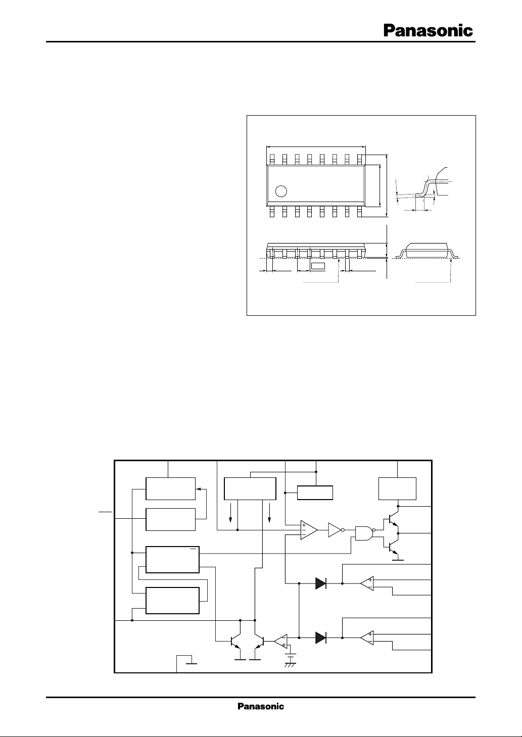
16 9
18
10.1±0.3
4.2±0.3
6.5±0.3
■ Features
• Operating supply voltage: 3.6 V to 34 V
• Totem pole output circuit: Output current of ±500 mA
• Built-in bootstrap circuit
• N-channel power MOSFET can be directly driven
• Built-in two error amplifier circuits allow both the
voltage and current control
• Incorporating on/off functions (active-high control input, standby mode current is 5 µA or less)
• Built-in timer latch short-circuit protection circuit
• Maximum oscillation frequency: 500 kHz
Note)*: The voltage is limited to the range of 3.6 V to 17 V if used in a step-down circuit.
*
(0.605)
1.27
Seating plane
0.40±0.25
0.1±0.1 1.5±0.2
SOP016-P-0225A
■ Applications
• LCD displays, digital still cameras, and PDAs
(0.15)
0.3
Unit: mm
(0° to 10°)
Seating plane
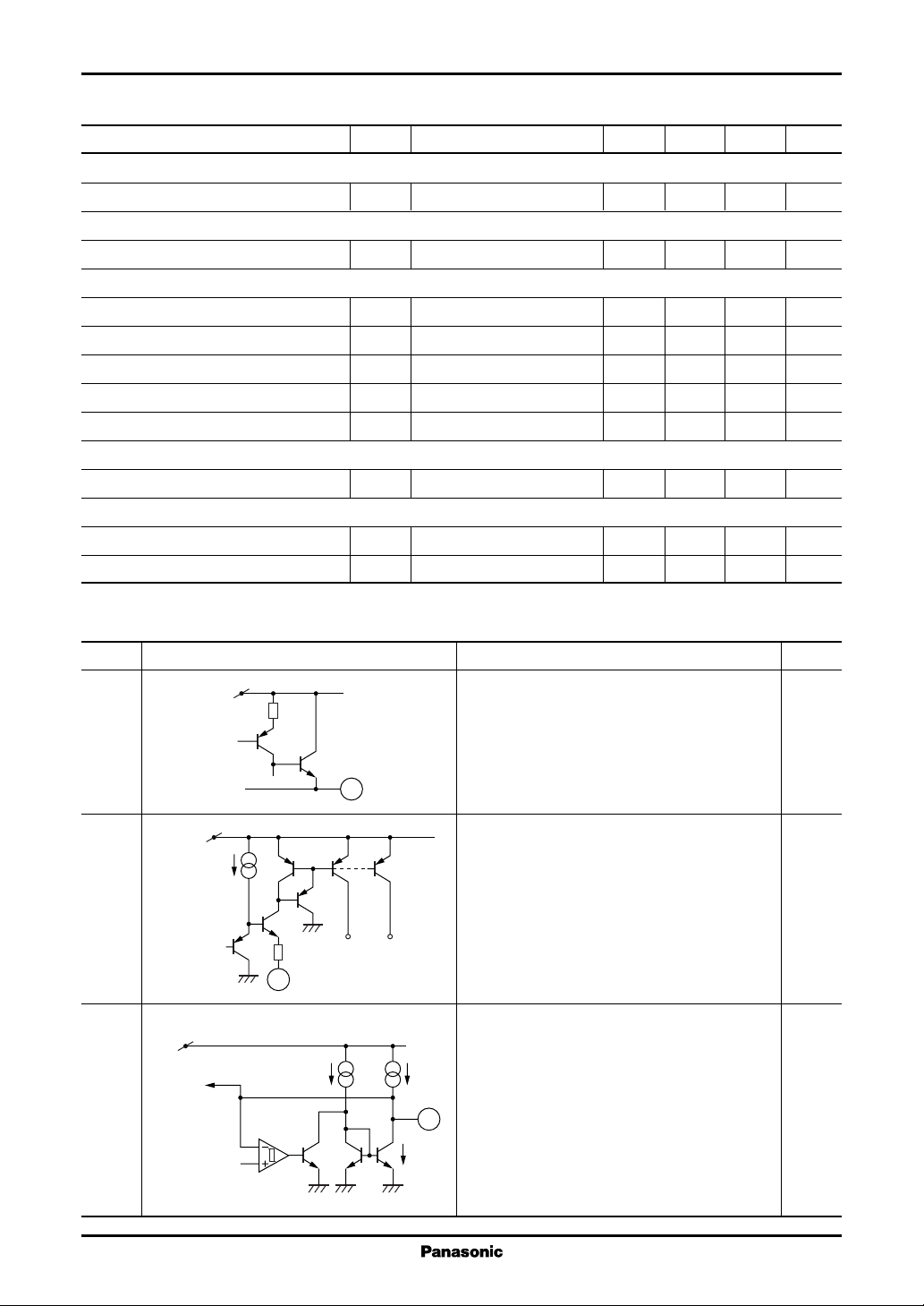
■ Block Diagram
Off
S.C.P.
16
5
REF
V
1
V
REF
2.57 V
On/off
active-high
R
U.V.L.O.
S
R
Latch
S
12
Q
Q
Q
GND
DTC
4
Constant
current source
S.C.P.
comp.
CT
3
PWM comp.
2
OSC
RT
Error amp. 1
Error amp. 2
CC
V
15
Bootstrap
14
13
11
10
CB
Out
8
FB1
6
IN+1
7
IN−1
9
FB2
IN+2
IN−2
1
Page 2

AN8041S Voltage Regulators
■ Pin Descriptions
Pin No. Symbol Description
1V
Reference voltage output pin
REF
2 RT Pin for connecting oscillator
timing resistor
3 CT Pin for connecting oscillator
timing capacitor
4 DTC Dead-time control pin
5 S.C.P. Pin for connecting the time constant
setting capacitor for short-circuit
protection
6IN+1
Error amplifier 1 noninverted input pin
■ Absolute Maximum Ratings
Parameter Symbol Rating Unit
Supply voltage V
Off terminal application voltage V
Error amplifier input voltage V
DTC terminal application voltage V
Out terminal application voltage V
CB terminal application voltage V
Out terminal constant output current I
Out terminal peak output current I
Power dissipation
Operating ambient temperature
Storage temperature
Note)*: Expect for the operating ambient temperature and storage temperature, all ratings are for Ta = 25°C.
*
*
*
CC
OFF
I
DTC
OUT
CB
O
O(PEAK)
P
D
T
opr
T
stg
Pin No. Symbol Description
7IN−1 Error amplifier 1 inverted input pin
8 FB1 Error amplifier 1 output pin
9 FB2 Error amplifier 2 output pin
10 IN−2 Error amplifier 2 inverted input pin
11 IN+2
Error amplifier 2 noninverted input pin
12 GND Grounding pin
13 Out Output pin
14 CB Bootstrap output circuit
15 V
Power supply voltage application pin
CC
16 Off On/off control pin
35 V
35 V
− 0.3 to V
− 0.3 to V
REF
REF
35 V
35 V
±100 mA
±500 mA
143 mW
−30 to +85 °C
−40 to +125 °C
V
V
■ Recommended Operating Range
Parameter Symbol Range Unit
Supply voltage (when using step-down circuit) V
Supply voltage (when using step-up circuit) V
Oscillation frequency f
Oscillator timing resistance R
Oscillator timing capacitance C
Error amplifier input voltage V
Reference voltage output current I
2
CC
CC
OUT
IN
REF
3.6 to 17 V
3.6 to 34 V
5 to 500 kHz
T
T
5.1 to 30 kΩ
100 to 10 000 pF
− 0.1 to +0.8 V
−1 to 0 mA
Page 3

Voltage Regulators AN8041S
■ Electrical Characteristics at VCC = 12 V, RT = 15 kΩ, CT = 120 pF, Ta = 25°C
Parameter Symbol Conditions Min Typ Max Unit
Reference voltage block
Output voltage V
REFIREF
Input regulation with input fluctuation Line VCC = 3.6 V to 34 V 725mV
Load regulation Load I
Output voltage V
TC1Ta
temperature characteristics 1
Output voltage V
TC2Ta
temperature characteristics 2
Output short-circuit current I
OS
U.V.L.O. block
Circuit operation start voltage V
Hysteresis width V
UON
HYS
Error amplifier block
Input offset voltage V
Input bias current I
Common-mode input voltage range V
High-level output voltage 1 V
Low-level output voltage 1 V
Output sink current I
Output source current I
Open-loop gain A
IO
B
ICR
EH
EL
SINK
SOURCEVFB
G
Dead-time control circuit block
Input current I
Low-level input threshold voltage V
High-level input threshold voltage V
DTC
DT-L
DT-H
Output block
Oscillation frequency f
OUT
Output duty ratio Du R
Low-level output voltage V
High-level output voltage V
Frequency f
OLIO
OHIO
dV
supply voltage characteristics VCC = 3.6 V to 34 V
Frequency f
dT1fOUT
temperature characteristics 1 Ta = −30°C to +25°C
Frequency f
dT2fOUT
temperature characteristics 2 Ta = 25°C to 85°C
= −1 mA 2.483 2.57 2.647 V
= − 0.1 mA to −1 mA 110mV
REF
= −30°C to +25°C ±1 %
= 25°C to 85°C ±1 %
−10 mA
2.8 3.1 3.4 V
60 140 220 mV
−6 6mV
−500 −25 nA
− 0.1 0.8 V
V
REF
− 0.3 V
REF
− 0.1
V
0.1 0.3 V
VFB = 0.9 V 8 mA
= 0.9 V −110 µA
70 dB
RT = 15 kΩ−14.8 −12.3 −9.8 µA
Duty = 0% 0.45 0.65 V
Duty = 100% 1.2 1.4 V
RT = 15 kΩ, 180 200 220 kHz
CT = 120 pF
= 75 kΩ 45 50 55 %
DTC
= 70 mA 1.0 1.3 V
= −70 mA VCB−2.0 VCB−1.0 V
f
= 200 kHz, ±3 V
OUT
= 200 kHz, ±9 V
= 200 kHz, ±9 V
3
Page 4
AN8041S Voltage Regulators
■ Electrical Characteristics at VCC = 12 V, RT = 15 kΩ, CT = 120 pF, Ta = 25°C (continued)
Parameter Symbol Conditions Min Typ Max Unit
Bootstrap circuit block
Input standby voltage V
Oscillator block
RT terminal voltage V
Short-circuit protection block
Input threshold voltage V
Input standby voltage V
Input latch voltage V
Charge current I
Comparator threshold voltage V
On/off control block
Threshold voltage V
Whole device
Total consumption current I
Standby current I
CC(SB)
INCBICB
RT
THPC
STBY
IN
CHG
THL
TH
CC
= −70 mA
VCC−1.2 VCC−1.0 VCC− 0.8
0.37 V
0.70 0.75 0.80 V
30 120 mV
30 120 mV
−2.76 −2.3 −1.84 µA
1.82 V
0.8 2.0 V
3.9 5.0 mA
5 µA
V
■ Terminal Equivalent Circuits
Pin No. Equivalent circuit Description I/O
1V
V
CC
1
2 RT:
3 CT:
V
REF
V
REF
To PWM input
OSC
comp.
100 Ω
2
RT (≈ 0.37 V)
DTC S.C.P.
I
O
3
2I
O
:O
REF
The reference voltage output terminal
(2.57 V (allowance: ±3%)).
Incorporating short-circuit protection against
GND.
The terminal used for connecting a timing resistor to set oscillator's frequency.
Use a resistance value within the range of 5.1 kΩ
to 30 kΩ.
The terminal voltage is approx. 0.37 V.
The terminal used for connecting a timing capacitor to set oscillator's frequency.
Use a capacitance value within the range of 100
pF to 10 000 pF.
For frequency setting method, refer to the
" Application Notes, [3] Function descriptions "
section. Use an oscillation frequency in the range
of 5 kHz to 500 kHz.
4
Page 5
Voltage Regulators AN8041S
■ Terminal Equivalent Circuits (continued)
Pin No. Equivalent circuit Description I/O
4 DTC:
5 S.C.P.:
6IN+1: I
7IN−1: I
8 FB1: O
9 FB2: O
V
REF
RT
V
REF
I
CHG
To U.V.L.O.
V
REF
V
REF
V
REF
The terminal for connecting a resistor and ca-
PWM
comparator
input
I
4
DTC
C
DTC
R
DTC
pacitor to set the dead-time and soft start period
of PWM output. Input current I
is determined
DTC
by the timing resistor RT , so that dispersion and
fluctuation with temperature are suppressed. It
is approx. −12.3 µA when R
V
=
RT
×1[A]
RT2
I
DTC
= 15 kΩ.
T
The terminal for connecting a capacitor to set the
time constant of soft start and timer latch shortcircuit protection circuit.
0.75 V
Latch
S
R
Q
Use a capacitance value in the range of more than
1 000 pF.
The charge current I
is determined by the
CHG
timing resistor RT , so that dispersion and fluctuation with temperature are suppressed. It is
5
approx. −1.3 µA when R
V
=
RT
×1[A]
RT11
I
CHG
= 15 kΩ.
T
The noninverted input terminal of the error amplifier 1.
For common-mode input, use in the range of
− 0.1 V to +0.8 V.
The inverted input terminal of the error amplifier 1.
67
For common-mode input, use in the range of
− 0.1 V to +0.8 V.
The output terminal of the error amplifier 1.
Source current
8
Sink current
Source current: approx. −120 µA
Sink current : approx. 8 mA
Correct the frequency characteristics of the gain
and the phase by connecting a resistor and a capacitor between this terminal and IN−1 terminal.
The output terminal of the error amplifier 2.
Source current
9
Sink current
Source current: approx. −120 µA
Sink current : approx. 8 mA
Correct the frequency characteristics of the gain
and the phase by connecting a resistor and a capacitor between this terminal and IN−2 terminal.
5
Page 6

AN8041S Voltage Regulators
■ Terminal Equivalent Circuits (continued)
Pin No. Equivalent circuit Description I/O
10 IN−2: I
11 IN+2: I
12 GND:
13 Out: O
14 CB: O
15 V
V
REF
The inverted input terminal of the error amplifier 2.
For common-mode input, use in the range of
− 0.1 V to +0.8 V.
The noninverted input terminal of the error amplifier 2.
1110
For common-mode input, use in the range of
− 0.1 V to +0.8 V.
12
V
CC
Grounding terminal.
Totem pole type output terminal.
A constant output current of ±100 mA and a peak
output current of ±1 A can be obtained.
14
Bootstrap output terminal.
13
When using step-down circuit, connect the capacitor for boost between this terminal and the
n-channel MOSFET source side of the switching
device.
When using step-up circuit, short circuit this
terminal with VCC terminal.
:I
15
CC
Power supply application terminal.
16 Off: I
On/off control terminal.
High-level input: normal operation
(V
> 2.0 V)
OFF
Low-level input: standby condition
(V
< 0.8 V)
OFF
16
17 kΩ
13 kΩ
Internal
circuit
Start/Stop
The total consumption current can be suppressed
to 10 µA or less.
6
Page 7

Voltage Regulators AN8041S
■ Application Notes
[1] Main characteristics
600
P
T
D
a
Oscillation frequency Timing capacitance
500
518
500
400
(mW)
D
360
300
207
200
143
Power dissipation P
100
0
0 25 150
50 75 85 100 125
Ambient temperature Ta (°C)
Glass epoxy board
(50 × 50 × 0.8t mm3)
R
= 263°C/W
th(j−a)
= 380 mW (25°C)
P
D
Independent IC
without a heat sink
R
= 278°C/W
th( j−a)
PD = 360 mW (25°C)
(kHz)
100
OUT
RT = 15 kΩ
Oscillation frequency f
10
5
100 1 000 10 000
RT = 5.1 kΩ
Timing capacitance CT (pF)
Oscillation frequency temperature characteristics Output duty ratio temperature characteristics
VCC = 12 V
205
(kHz)
200
OUT
195
190
Oscillation frequency f
185
VCC = 12 V
54
52
50
48
Output duty ratio Du (%)
46
−50 −25 100
0 25 50 75
Ambient temperature Ta (°C)
−50 −25 100
0 25 50 75
Ambient temperature Ta (°C)
Internal reference voltage temperature characteristics Output duty ratio DTC terminal voltage
2.57
(V)
REF
2.56
2.55
2.54
2.53
Internal reference voltage V
−50 −25 100
0 25 50 75
Ambient temperature Ta (°C)
VCC = 12 V
100
80
60
40
Output duty ratio Du (%)
20
0.2 0.4 1.4
0.6 0.8 1.0 1.2
DTC terminal voltage (V)
VCC = 12 V
7
Page 8

AN8041S Voltage Regulators
■ Application Notes (continued)
[2] Timing chart
1. PWM comparator operation waveform
Off terminal voltage
Supply voltage (V
Internal reference voltage (V
Power supply
Triangular wave (CT)
on
S.C.P. terminal voltage
Out terminal waveform
2. Short-ciruit protection operation waveform
)
CC
Error amplifier 1 output (FB 1)
)
REF
Error amplifier 2 output (FB 2)
DTC terminal voltage
Soft start operation Maximum duty
High
Low
3.6 V
2.57 V
1.82 V
1.32 V
0.44 V
0.03 V
High
Low
Internal reference voltage
Error amplifier output (FB1)
Short-circuit protection comparator
threshold level
DTC terminal voltage
Error amplifier output (FB2)
Triangular wave (CT)
Out terminal waveform
S.C.P. terminal voltage
Short-circuit protection
comparator output
8
2.57 V
1.82 V
1.32 V
0.44 V
High
Low
0.75 V
0.03 V
t
PE
High
Low
Page 9

Voltage Regulators AN8041S
■ Application Notes (continued)
[3] Function descriptions
1. Reference voltage block
This block is composed of the band gap circuit, and outputs the temperature-compensated 2.57 V reference
voltage to the V
and used as the operating power supply for the IC inside. It is possible to take out a load current of up to −1 mA.
2. Triangular wave oscillation block (OSC)
The triangular wave which swings from the upper limit value V
value V
OSCL
the C
terminal (pin 2) and RT terminal (pin 3) respectively. The oscillation frequency can be arbitrarily decided
T
by the value of timing capacitor C
by the following calculations:
f
=
OSC
1.7 × V
I
=
O
Since V
therefore f
Example) When CT = 100 [pF], RT = 15 [kΩ],
It is possible to use the circuit in the recommended operating range of 5 kHz to 500 kHz of the oscillation
frequency. In addition, when the oscillation frequency becomes high, overshoot and undershoot are generated due
to the operation delay of the triangular oscillation comparator. Care should be taken because the actual measurement values deviate from the above calculation values.
In the case of this IC, the output source current of S.C.P. terminal and DTC terminal are set by the timing resistor
R
externally attached to RT terminal. For this reason, the AN8041S can not be used as a slave IC when multiple
T
ICs are synchronously operating in parallel.
terminal (pin 16). The reference voltage is stabilized when the supply voltage is 3.6 V or higher,
REF
of approximately 1.32 V to the lowest limit
OSCH
of approximately 0.44 V will be generated by connecting a timing capacitor CT and a resistor RT to
1
t1 + t
R
T
2
RT
CTH
OSC
=
2 × CT × (V
1.7 × 0.37
=
− V
CTL
≈
2.80 × C
and resistor RT connected externally. The oscillation frequency f
T
I
O
− V
)
CHL
t
t
[Hz]
T
Charging
1
2
Discharging
R
T
= 0.88 V,
CTH
1
× R
T
V
V
is obtained
OSC
= 1.32 V typ.
CTH
= 0.44 V typ.
CTL
T
f
≈ 238 [kHz].
OSC
Figure 1. Triangular wave oscillation waveform
3. Error amplifier 1 block and error amplifier 2 block
DC-DC output voltage and a detected lamp current of back-light are amplified through the PNP transistor input
type error amplifier, and the amplified signal are inputted to PWM comparator.
Figure 2 shows the connection method of the error amplifier when the backlight inverter is controlled. Select
the connection of error amplifier 1 block or 2 block arbitrarily.
The common-mode input range is from − 0.1 V to +0.8 V. The voltage which is resistor-dividing of the reference
voltage is given to the noninverted input. Also, any desired gain setting and phase compensation can be obtained
by connecting the feedback resistor and capacitor from the error amplifier output terminals (pin 8 and pin 9) to the
inverted input terminals (pin 7 and pin 10).
The overshoot at operation start due to feedback delay can be suppressed by providing the large output source
current (110 µA) and the large output sink current (8 mA).
The output voltage V
and the detection voltage of the lamp current VC1 are given from the following
OUT
calculation:
R
V
= V
IN+
V
= V
OUT
VC1= V
REF
IN+1
IN+2
×
R3 + R
R1 + R
×
R5 + VR + R
×
4
R
2
R5 + V
4
2
6
R
9
Page 10

AN8041S Voltage Regulators
■ Application Notes (continued)
[3] Function descriptions (continued)
3. Error amplifier 1 block and error amplifier 2 block (continued)
DC-AC
V
OUT
R2R1R4
R3
V
REF
IN+1
IN−1
16
6
7
R
NF1
CT
Error amp. 2Error amp. 1
DTC
9
R
FB1 8
FB2
NF2
inverter
L
A
M
V
C1
D
SBD
C
1
P
1
R7
IN+211
IN−210
Backlight
control
R6
V
R
R5
Error amplifier 1
block
C
NF1
C
NF2
Error amplifier 2
block
DC-DC
converter
output voltage
detection
Figure 2. Connection method of the error amplifier 1 and 2
Backlight lamp
current detection
The control modes of backlight are described below:
1) Power-on mode
When the power supply is turned on, the DC-DC converter which is connected to the error amplifier 1 block
starts the control.
The output voltage V
which has been set by the equation in the previous page is reached, and the high
OUT
voltage of several kV is generated in the lamp through the DC-AC inverter, and the backlight is lighted up.
During this period, since the lamp current does not flow in the error amplifier 2 block, the error amplifier output
(FB2) becomes high-level, so that its control does not work.
2) Normal control mode
When the backlight is turned on, discharging starts and the current starts to flow in the resistor R7.
When the voltage V
and volume control V
amplifier 2 block. The output voltage of the DC-DC converter V
rectified by diode D1, and capacitor C1 reaches the voltage set by resistors R5, R6,
C1
; The control function is switched over from the error amplifier 1 block to the error
R
decreases to a voltage lower than the set
OUT
voltage, and the lamp voltage is maintained at several hundred volts.
3) Light-regulation operation mode
For the light regulation of the backlight, the "voltage light-regulation" method is used, and the light is
regulated by the input voltage of the inverter. By adding volume V
amplifier 2 block to make the detection voltage V
variable, the input voltage of the inverter is regulated so
C1
to the inverted input terminal of error
R
as to make the lamp current variable for light regulation.
Also, the addition of the volume to the noninverted input side of the error amplifier makes the light
regulation possible.
• Usage notes
When this IC is used to control the
DC-DC converter, one of two error
amplifiers is not used. Connection
should be made so that the FB terminal is fixed to high-level as shown in
figure 3.
Error amp. 2
9
FB terminal
open
11
IN+2
IN−210
To reference voltage terminal
FB terminal → High-level
V
> V
IN+2
IN−2
10
Figure 3. Connection when the error amplifier 2 block is not used
Page 11

Voltage Regulators AN8041S
■ Application Note (continued)
[3] Function descriptions (continued)
4. Timer latch short-circuit protection circuit
When the short-circuit or overload of the power supply output continues for a certain period, this circuit
prevents the parts such as external main switch device, flywheel diode, the choke coil from destruction or deterioration.
The short-circuit protection circuit is shown in figure 4. The timer latch short-circuit protection circuit detects
the output level of the error amplifier 1 and 2 blocks. When either the DC-DC converter output voltage or the lamp
current detection voltage is stable, the output of that error amplifier is stabilized and the short-circuit protection
comparator also maintains balance.
When the load conditions are suddenly changed, and both of the outputs of the error amplifier 1 block and 2
block (FB1, FB2) become 1.82 V or higher, the short-circuit protection comparator outputs low-level and cut off
the transistor Q1, thereby the external capacitor C
given by the following equation:
t
VPE = V
STBY
+ I
0.75 V = 0.03 V + I
t
CS = I
CHG
I
is constant current which is determined by the timing resistor RT of the oscillator. It becomes approximately
CHG
2.3 µA when R
I
=
CHG
×
0.72
= 15 kΩ.
T
VRT × 1
R
× 11
T
PE
When the external capacitor C
CHG
×
CHG
[F]
[A]
PE
[V]
C
S
t
PE
×
C
S
is charged to approximately 0.75 V, the latch circuit is set to fix the totem pole
S
output terminal to low-level and sets the dead-time to 100%.
When the latch circuit is set, the S.C.P. terminal voltage is discharged to approximately 30 mV. However, once
the latch circuit is set, it is not reset unless the power supply is turned off.
of the S.C.P. terminal (pin 5) starts charging with current I
S
CHG
IN+1
IN−1
FB1
IN+2
IN−2
FB2
6
7
8
Error amp. 2
11
10
9
S.C.P. comp.
1.82 V
I
CHG
Q1
S.C.P.
SQ
R
Latch
Q2
5
C
S
Q
V
REF
Output cut-off
Error amp. 1
Figure 4. Short-circuit protection circuit
5. Low input voltage malfunction prevention circuit (U.V.L.O.)
When the supply voltage is dropped under the transient condition such as power-on or operation stop, this
circuit protects the system from destruction or deterioration due to the malfunction of the control circuit.
This circuit detects the internal reference voltage which varies according to the supply voltage level. During
the period from the time when the supply voltage starts to rise and to the time when it reaches 3.1 V, it keeps the deadtime of the Out terminal (pin 13) to 100% and maintains the DTC terminal (pin 4) and the S.C.P. terminal (pin 5) at
low-level. When the supply voltage falls, it holds the hysteresis width of 140 mV and operates at a voltage under
2.96 V.
11
Page 12

AN8041S Voltage Regulators
■ Application Notes (continued)
[3] Function descriptions (continued)
6. Remote circuit
The IC control function can be turned on or off by the external control. When the voltage of Off terminal (pin
16) is set under approximately 0.8 V, the internal reference voltage falls to stop the IC control function, and decrease
the circuit current to a value under 5 µA, When the voltage of Off terminal is set at a value higher than approximately
2.0 V, the internal reference voltage rises, and starts the control operation.
7. PWM comparator block
The PWM comparator controls the on-period of the output pulse according to the input voltage. While the
voltage of triangular wave of the CT terminal (pin 3) is lower than any one of the output of the error amplifier 1
and 2 block (pin 8 and pin 9) and the voltage of the DTC terminal (pin 4), it sets the Out terminal (pin 13) to highlevel so that the switching device (n-channel MOSFET) turns on .
The dead-time is set by regulating the DTC terminal voltage V
The DTC terminal is of a constant current output using the resistor R
connecting the external resistor R
At the oscillation frequency f
and 100% when V
= 1.32 V typical.
DTC
However, pay attention to the peak value V
between the DTC terminal and GND terminal.
DTC
of 200 kHz, the output duty ratio becomes 0% when V
OSC
and the trough value V
CTH
overshoot and undershoot amount differ depending on the oscillation frequency.
as shown in figure 5.
DTC
, so that the V
T
of the triangular wave because their
CTL
is regulated by
DTC
= 0.44 V typical,
DTC
CT waveform
DTC waveform
t
OFFtON
V
CTH
V
DTC
V
CTL
V
REF
I
DTC
CT
PWM
FB
Out waveform
Off On Off
R
DTC
DTC
C
DTC
Figure 5. Setting the dead-time
The output duty ratio Du and the DTC terminal voltage V
t
t
ON
V
=
V
ON
+ t
OFF
− V
DTC
CTL
− V
CTH
CTL
V
≈ 1.32 [V], V
CTH
Therefore I
× 100 [%] I
× 100 [%]
= 200 [kHz] (RT = 15 kΩ, CT = 150 pF), R
OSC
≈ 0.44 [V], V
CTL
≈ 12.3 [µA]
DTC
V
≈ 0.925 [V]
DTC
V
DTC
DTC
Du =
Example) When f
V
=
= I
= VRT ×
≈ 0.37 [V]
DTC
are given in the following equation:
DTC
1
RT
×
R
2
DTC
DTC
R
T
[A]
×
DTC
1
[A]
2
= 75 [kΩ]
R
DTC
T
× R
Du ≈ 55.1 [%]
In addition, the operation delay of the PWM comparator, the deviation of the peak and trough triangular
oscillation value may cause the deviation of the actual measurements value from the theoretical value. So, regulation on IC-mounted PCB should be required.
By adding the external resistor R
and capacitor C
DTC
, the soft start function can be installed, which
DTC
gradually broadens the on-period of the output pulse at the time of the power supply operation start. The soft start
operation prevents the overshoot of DC-DC comparator output.
12
Page 13

Voltage Regulators AN8041S
■ Application Notes (continued)
[3] Function descriptions (continued)
8. Output block, bootstrap circuit
In the case of the step-down type DC-DC converter control, the bootstrap circuit is required if n-channel
MOSFET is used as the switching device.
The bootstrap circuit is used for keeping the voltage between the gate and the source higher than the gate
threshold voltage of n-channel MOSFET by increasing the high-level of the Out terminal (pin 13) to a level higher
than V
circuit are shown in figure 6, and the operation waveform in figure 7.
when turning on the n-channel MOSFET. The output block including the external circuit and the bootstrap
CC
V
S
SBD
V
GS
V
CB
V
CB
PWM comparator
CT
DTC
FB1
FB2
M1
CC
V
V
15
D1
D1
Q1
14
I
1
CB
I
2
Out13
Q2
OUT
Figure 6. Output block and bootstrap circuit
V
CC
CB terminal waveform
Turn-on
Out terminal waveform
0 V
M1 source-side waveform
t
1
M1 Off
t
2
M1 On
Figure 7. Bootstrap circuit operation waveform
The bootstrap circuit operation is described below.
1) N-channel MOSFET (M1) off time: t
1
While the M1 is off, energy is being supplied from the schottky barrier diode (SBD) to the choke coil, and
the M1 source side voltage V
is fixed to −VF . The capacitor for boost CB is charged from the VCC terminal
S
(pin 15) through the diode inside the IC (D1). The CB terminal voltage (pin 14) V
equation:
V
= −V
S
F
VCB = V
CC −VD1
VF: forward voltage of SBD
V
: forward voltage of D1
D1
Therefore, the charged voltage of boost C
V
CB−VS
= V
CC −VD1+VF
is given by the following equation:
B
Turn-off
t
3
M1 Off
V
CBH
V
OH
VCC − V
DS(ON)
VCC − 0.7 [V]
V
OL
−V
F
is given by the following
CB
[V]
13
Page 14

AN8041S Voltage Regulators
■ Application Notes (continued)
[3] Function descriptions (continued)
8. Output block, bootstrap circuit (continued)
2) N-channel MOSFET (M1) turn-on time: t
When the PWM comparator output reverses, the Out terminal (pin 13) is switched over to high-level. The
Out terminal voltage V
rises toward the CB terminal voltage.
O
VO = VCB−VCE (sat)
At that time, M1 voltage between the gate and source becomes:
V
= VO+V
GS
F
When the Out terminal voltage VO rises to the gate threshold voltage, the M1 is turned on. The M1 source-
side voltage after the turn-on rises to the value expressed in the following equation:
V
= V
S
CC −VDS(ON)
Since the bootstrap capacitor CB is connected between the M1 source-side and the CB terminal, the CB
terminal voltage is capacitance-coupled, and rises according to the M1 source-side voltage. It is expressed in
the following equation:
V
= VS +V
CB
CC −VD1+VF
= 2 × V
CC −VD1+VDS(ON)+VF
3) N-channel MOSFET (M1) turn-off time: t
The Out terminal voltage drops to the saturation voltage of the transistor Q1 and it is turned off.
The M1 source side voltage decreases to −V
coupled, and drops to V
volt, and returns to the condition described in a).
CC −VD1
2
3
, and in the same way the CB terminal voltage is capacitance-
F
• Bootstrap circuit usage notes
(1) Operating supply voltage range when the step-down circuit is used
When the step-down circuit is used for the DC-DC converter control : As described in the above, when
the n-channel MOSFET of the switching device turns on, the voltage of CB terminal (pin 14) rises to the voltage
about two times higher than the V
. Since the allowable applied voltage for the CB terminal is 35 V, use the
CC
boost circuit at an operating supply voltage of 3.6 V or more.
V
= 2 × VCC − VD1 − V
CB
35 + VD1 + V
V
<
CC
DS(ON)
2
+ VF < 35 [V]
DS(ON)
− V
F
[V]
< 17 [V]
(2) Value setting for bootstrap capacitor
The bootstrap capacitor is capacitors-coupled with the n-channel MOSFET source-side at its turn-on time
to increase the CB terminal voltage over the V
. At this time, the bootstrap capacitor is discharged by the
CC
n-channel MOSFET gate drive current. If the capacitance value of the bootstrap capacitor is set at too low
value, it causes the efficiency decrease due to increase in switching loss.
Therefore, set the capacitance at a sufficiently high value compared with the n-channel MOSFET gate
input capacitance.
CB >> Ciss
Study with the actual mounting board and set the optimum value.
(3) CB terminal connection when the booster circuit is used
In the case of using the step-up type DC-DC converter control, the bootstrap circuit is not required since
the n-channel MOSFET source side is grounded. Therefore, use it by short-circuiting the CB terminal (pin
14) to the V
terminal (pin 15).
CC
For that reason, the operating supply voltage range is 3.6 V to 34 V in the case of using the step-up circuit
type.
14
Page 15

Voltage Regulators AN8041S
■ Application Circuit Examples
• Inverter control for liquid crystal backlight
Off
S.C.P.
104 pF
V
1
0.72 V
16
5
3.3 kΩ
8.2 kΩ
V
V
2.57 V
On/Off
active-high
R
U.V.L.O.
S
R
Latch
S
REF
1
REF
GND 12
0.1 µF
91
kΩ
Q
Q
Q
0.01 µF
DTC4
12 µA
Constant
current source
CT3
2.3 µA
S.C.P.
comp.
1.82 V
120 pF
RT2
OSC
PWM comp.
In
15 kΩ
Error amp. 1
Error amp. 2
CC
V
15
Bootstrap
SBD
CB14
L
A
M
P
Out13
FB18
IN+16
IN−17
FB29
18 kΩ
3 kΩ
IN+211
IN−210
V
1
SBD
• DC-DC converter control (step-up circuit example)
V
1
Off
S.C.P.In5
16
REF
V
1
V
REF
2.57 V
On/Off
active-high
R
U.V.L.O.
S
R
Latch
S
DTC4
CT3
Constant
current source
PWM comp.
Q
Q
Q
S.C.P.
comp.
1.82 V
GND 12
RT2
OSC
Bootstrap
Error amp. 1
Error amp. 2
SBD
Out
CC
V
15
CB14
Out13
FB18
IN+16
IN−17
FB29
IN+211
IN−210
V
1
15
 Loading...