

Page 1
Voltage Regulators
AN8038, AN8038S
AC-DC switching power supply control IC
with RCC local resonance circuit for
improved conformance with
energy conservation laws
■ Overview
The AN8038 and AN8038S are self-excited AC-DC
switching power supply control IC that adopt RCC local
resonance control. These ICs are designed to achieve high
efficiency over a wide range of loads (light loads at the
standby mode to heavy loads) for improved conformance
with energy conservation laws, and support input levels
used worldwide. They are particularly appropriate for use
in AV and OA equipments.
■ Features
• Supports improved conformance with energy conser-
vation laws by providing two operating modes.
With external resistors, it is possible to set the operating
point at which the modes change over according to the
load power, as shown below.
1.Continuous (RCC) mode
High efficiency achieved with local resonance operation (zero cross detection).
2.Discontinuous mode (standby) mode
Reduced switching loss and standby power due to reduced frequency
• Input voltage correction function. This function corrects
the maximum on-period in a manner inversely proportional to the input voltage.
• Built-in overvoltage protection function (detects at V
• Pulse-by-pulse overcurrent protection function (single detection per one cycle)
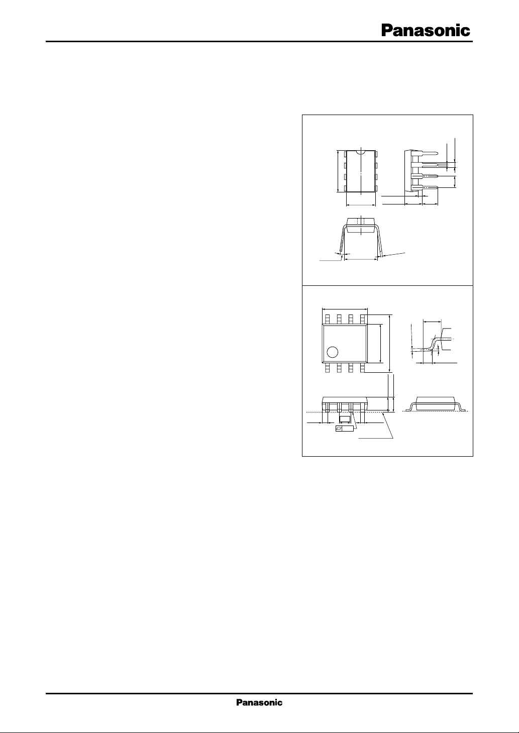
• Packages: 8-pin DIP ··· AN8038
8-pin SOP··· AN8038S
CC
pin)
AN8038 Unit: mm
3° to 15°
AN8038S Unit: mm
(0.60)
1
2
3
9.4±0.3
4
6.3±0.3
7.62±0.25
DIP008-P-0300B
5.01±0.20
1.27
0.10
Seating plane
SOP008-P-0225C
8
7
6
5
0.51 min.
3.8±0.25
.1
0
+
5
.0
0
–
0.15
58
0.15±0.10
6.40±0.20
4.30±0.20
41
1.75 max.
1.45±0.10
+0.10
0.40
–0.05
(3.45)
(1.05)
0.5±0.1
0° to10°
0.50±0.20
1.2±0.25
2.54
■ Applications
• Facsimiles and other OA equipment
• Printers and other personal computer peripheral equipment
• AV equipment
1
Page 2
AN8038, AN8038S Voltage Regulators
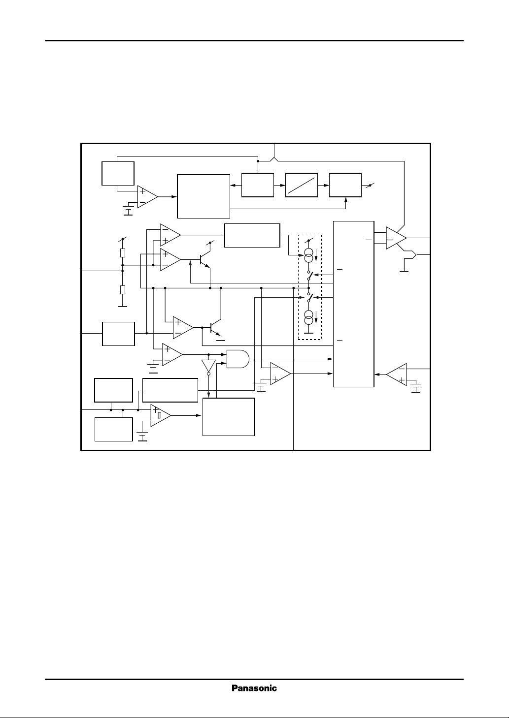
■ Block Diagram
CC
V
8
RSTB
IFB
TR
2
4
High-side
1
Low-side
OVP
17.5
kΩ
17.5
kΩ
I/V
conv .
clamp
clamp
7 V
4.2 V
OVP
S
V
FB
Current
reviser (ITR)
0.25 V
(SD latch)
RQ
S
(TR latch)
INIT
R
Q
Current
reviser (IFB)
1.0 V
Start
Stop
3
V
REF
7 V
Q
In
In
Q
Out
7
Out
6
GND
drive
Q
Q
Q
CF
latch
Q
T
ON
S
T
OFF
R
R
5
CLM
− 0.2 V
CF
2
Page 3

Voltage Regulators AN8038, AN8038S
■ Pin Descriptions
Pin No. Symbol Description
1 TR Transformer reset. When a transformer reset is detected, i.e., a low level is input to this pin, the IC
output goes high.
However, the transformer reset signal is ignored during the minimum off-period determined by
the CF pin. The maximum on-period is also corrected according to the current flowing out of this
pin.
2 RSTB Adjusts the light-load detection level that determines the when the IC switches from RCC to
discontinuous operation. When the voltage (V
signal from IFB pin goes up higher than this pin, minimum off-period current at CF pin decreases,
and operating frequency decreases.
The detection level can be adjusted arbitrarily using an external pull-down resistor.
3 CF Connection for the capacitor that determines the on and off periods for the IC output (Out).
4 IFB Input for the current feedback signal from the power supply output photocoupler
5 CLM Input of the pulse-by-pulse overcurrent protection circuit. Normally, it will be necessary to add
an external filter for this input.
6 GND Ground
7V
8V
Output to drive a power MOSFET directly
OUT
Power supply. This pin watches VCC , and has operating threshold voltages for the start, stop,
CC
OVP, and OVP reset levels.
) which is I-V conversion of current feedback
FB
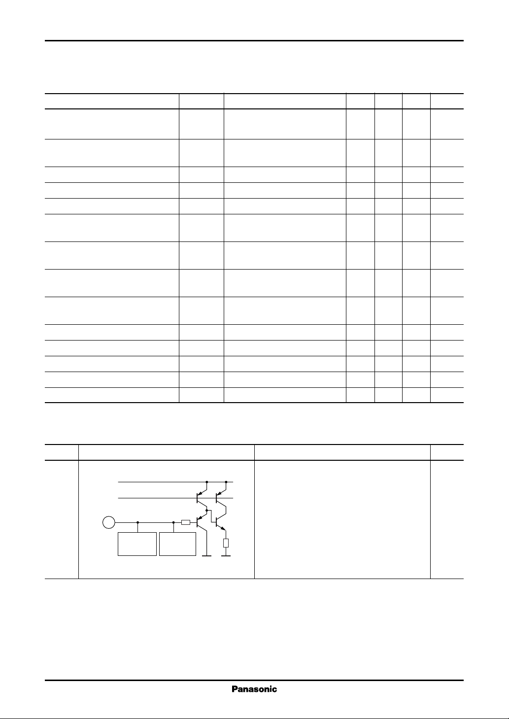
■ Absolute Maximum Ratings
Parameter Symbol Rating Unit
Supply voltage V
Peak output current I
CC
OP
28 V
−1, +2A
Power dissipation AN8038 PD (Ta = 25°C) 500 mW
(Independent IC PD (Ta = 85°C) 260
1
without a heat sink) AN8038S PD (Ta = 25°C) 306
PD (Ta = 85°C) 122
Operating temperature T
Storage temperature T
Note) *1: When mounted on a printed circuit board: 477 mW
2: When mounted on a printed circuit board: 191 mW
*
opr
stg
*
2
*
−30 to +85 °C
−55 to +150 °C
■ Recommended Operating Range
Parameter Symbol Range Unit
Supply voltage V
From the stop voltage to the OVP operating voltage V
CC
3
Page 4

AN8038, AN8038S Voltage Regulators
■ Electrical Characteristics at VCC = 18 V, Ta = 25°C
Parameter Symbol Conditions Min Typ Max Unit
Low voltage protection (U.V.L.O.) Start V
initial startup supply voltage.
Low voltage protection (U.V.L.O.) Stop V
operation stop supply voltage
Overvoltage protection (OVP) OVP V
operating supply voltage
Overvoltage protection (OVP) OVPC V
release supply voltage
Overvoltage protection (OVP) OVP I
operating time circuit current 1
Overvoltage protection (OVP) OVP I
operating time circuit current 2
Transformer reset detection (TR) TR V
threshold voltage
Transformer reset detection (TR) TR V
upper limit clamp voltage
Transformer reset detection (TR) TR V
lower limit clamp voltage
Transformer reset detection (TR) TR I
pin source current
Overcurrent protection (CLM) CLM V
threshold voltage
Oscillator (CF) maximum CF GI
on-period current gain
Oscillator (CF) maximum CF I
on-period current
Oscillator (CF) minimum CF I
off-period current 1
Oscillator (CF) minimum CF I
off-period current 2
Output oscillator frequency f
Standby pin (RSTB) voltage V
Standby operation (RSTB) RSTB V
threshold voltage
Current feedback pin (IFB) voltage V
Pre-startup low-level output voltage STB V
Low-level output voltage V
High-level output voltage V
Circuit current during startup 1 I
START1
Circuit current 1 OPR1 I
Circuit current 2 OPR2 I
4
CC
CC
CC
CC
CC1
CC2
TH
CLHITR
CLLITR
TR
TH
ONIFB
ON
OFF1IIFB
OFF2IIFB
OSC
RSTB
TH
IFB
OL
OL
OH
CC1VCC
CC2VCC
VCC = 22 V → 10 V 0.4 0.53 0.66 mA
VCC = 22 V → 18 V 1.3 1.7 2.1 mA
= 1 mA 1.2 1.5 1.8 V
= −1 mA − 0.3 − 0.15 0 V
VTR = 0.5 V −50µA
= Open 0.8 1.0 1.2
ITR = 0 mA 210 280 350 µA
= − 0.7 mA −1 560 −1 250 −940 µA
= −1.3 mA −70 −55 −40 µA
CF = 1 000 pF, ITR = −450 µA 105 140 175 kHz
I
= − 0.5 mA
IFB
I
= − 0.7 mA 5 5 .6 6 .2 V
IFB
VCC = 12 V 1.0 1.25 V
I
= 0.2 A 0.9 2.0 V
OUT
I
= − 0.1 A 15.5 16.3 V
OUT
= 10 V 6.1 8.7 11.3 mA
= 18 V 6.4 9.1 11.8 mA
12.9 14.4 15.9 V
8.0 8.9 9.8 V
18.7 20.5 22.3 V
6.6 7.5 8.4 V
0.15 0.25 0.35 V
−225 −205 −185 mV
3.2 3.5 3.8 V
0.3 0.5 0.7 V
120 190 280 µA
Page 5
Voltage Regulators AN8038, AN8038S
■ Electrical Characteristics at VCC = 18 V, Ta = 25°C (continued)
•
Design Reference Data
Note) The characteristics listed below are theoretical values based on the IC design and are not guaranteed.
Parameter Symbol Conditions Min Typ Max Unit
Low-voltage protection (U.V.L.O.) ∆V
start/stop supply voltage difference
Transformer reset (TR) detection TR ∆V
threshold hysteresis width
Oscillator (CF) upper limit voltage V
Oscillator (CF) lower limit voltage 1 V
Oscillator (CF) lower limit voltage 2 V
Maximum on-period t
Minimum off-period 1 t
Minimum off-period 2 t
Light-load oscillator frequency f
CLH
CFL1
CFL2
ON(max)
OFF(min)1IIFB
OFF(min)2IIFB
OSC2
Output rise time t
Output fall time t
TR output response time t
CLM output response time t
Circuit current during startup 2 I
TR
CLM
START2
CC
TH
I
= − 0.5 mA, CF = 1 000 pF 4.2 V
IFB
I
= − 0.5 mA, CF = 1 000 pF 1.0 V
IFB
I
= − 0.2 mA, CF = 1 000 pF 0.1 V
IFB
I
= − 0.2 mA, CF = 1 000 pF 12 µs
IFB
VTR = 0.1 V
= − 0.2 mA, CF = 1 000 pF 2.6 µs
VTR = 0.1 V
= −1.3 mA, CF = 1 000 pF 67 µs
ITR = −450 µA
I
= −1.3 mA, CF = 1 000 pF 15 kHz
IFB
ITR = −450 µA
r
f
10% to 90%, I
10% to 90%, I
= 0 mA 40 ns
OUT
= 0 mA 20 ns
OUT
Ta = −30°C to +85°C 100 190 300 µA
5.4 V
0.1 V
400 ns
100 ns
■ Terminal Equivalent Circuits
Pin No. Equivalent Circuit Description I/O
1 TR: I
V
REF
7 V
TR
1
High-side
clamp
Low-side
clamp
Transformer reset detection input.
When a transformer reset is detected, i.e., a low
level is input to this pin, the IC output goes high.
However, the transformer reset signal is ignored
if the signal is shorter than the minimum offperiod determined by the C
pin. Also note that
F
the maximum on-period is corrected according
to the source current.
5
Page 6
AN8038, AN8038S Voltage Regulators
■ Terminal Equivalent Circuits (continued)
Pin No. Equivalent Circuit Description I/O
2 RSTB:
Adjusts the light-load detection level that deter-
V
REF
17.5 kΩ
RSTB
Comp.
CF
17.5 kΩ
2
mines the time when the IC switches from RCC
to discontinuous operation. When the voltage
which is I-V conversion of current feedback signal goes up higher than this pin, operating frequency is reduced.
An arbitrary level can be set by inserting an
external pull-down resistor.
3 CF:
V
REF
I
OFF
Connection for the capacitor that determines the
on- and off-periods of the IC output (Out).
Comp.
The on- and off-periods are corrected by I
which is proportional to the flowing out cur-
V
FB
I
3
ON
rent at the TR pin, and I
to the current at IFB pin.
which corresponds
OFF
ON
CF
4 IFB: I
V
REF
× 5× 1
Connection for the photocoupler used for the
power supply output error-voltage feedback.
This input can decrease the photocoupler dark
V
FB
20 kΩ 1 kΩ
current by about 250 µA.
4
IFB
5 CLM: I
V
REF
Input to the pulse-by-pulse overcurrent protection circuit. Normally, we recommend adding
Comp.
an external filter for this input.
5
CLM
6 GND:
GND
6
IC ground.
6
Page 7
Voltage Regulators AN8038, AN8038S
■ Terminal Equivalent Circuits (continued)
Pin No. Equivalent Circuit Description I/O
7V
V
CC
:I
OUT
Output used to directly drive a power MOSFET.
A totem pole structure is adopted in this output
circuit.
The absolute maximum ratings for the output
7
V
OUT
current are:
Peak: +2 A, −1 A
DC: +200 mA, −100 mA
8V
V
CC
8
:
CC
Power supply.
This pin monitors supply voltage and has the
threshold for the start, stop, OVP, and OVP
reset levels.
■ Usage Notes
The circuit current during startup is set to a low level to minimize power loss due to the startup resistor. However,
V
ripple caused by the power transistor switching on and off may result in incorrect operation of the U.V.L.O. circuit
CC
and failure to start.
The figure shows the allowable range for V
V
ripple so that it remains within the allowable range.
CC
ripple. Insert a capacitor near the IC's V
CC
and GND pins to reduce
CC
3
2.5
2
1.5
ripple amplitude (V[p-p])
1
CC
V
0.6
0.5
0
Recommended
operating range
10
Allowable VCC ripple range
70 100 300 1 000 10 000
VCC ripple frequency (kHz)
7
Page 8

AN8038, AN8038S Voltage Regulators
■ Application Notes
[1] Timing charts
• Circuit diagram
CLM
• Normal control waveforms
(A) Bias winding voltage
0 V
(B) TR pin voltage
(C) CF pin voltage
4.2 V
V
0 V
RSTB
(B)
TRCF
V
CC
Out
(C)
On OnOn
Input voltage correction
: large, tON: short
E
IN
(D)
(G)
(A)
(F)(E)
OffOffOffOff
tON cannot be accepted
during t
OFF(min).
VFB voltage
Can be modified
with an external
resistor.
(D) Out pin voltage
Winding current
8
0 V
V
−1.5 V
CC
0 V
(F) Secondary
winding current
0 A
Off Off Off OffOn On On
(E) Primary
winding current
Heavy LightLoad
Continuous (RCC) mode Discontinuous mode
IFB correction
V
: large, t
FB
OFF(min)
: long
Page 9

Voltage Regulators AN8038, AN8038S
■ Application Notes (continued)
[1] Timing charts (continued)
• During pulse-by-pulse overcurrent operation
(A) Bias winding voltage
0 V
(B) TR pin voltage
(C) CF pin voltage
Can be modified
with an external
resistor.
(D) Out pin voltage
(E) Winding current
(G) CLM pin voltage
V
−1.5 V
CC
0 V
4.2 V
V
RSTB
VFB voltage
0 V
0 V
0 A
Light
0 V
On On OnOn
Rapid charging
during CLM
operation
Off Off Off OffOn On On On
Primary
winding
current
Secondary
winding
current
Load
OffOffOffOff
On-period
limitation during
CLM operation
Heavy
−205 mV
CLM threshold voltage
Overcurrent
detection
9
Page 10

AN8038, AN8038S Voltage Regulators
■ Application Notes (continued)
[2] Operation descriptions
1. Start/stop circuit block
• Startup mechanism
After the AC voltage is applied and the
supply voltage due to the current in the startup
resistor reaches the startup voltage and the IC
begins to operate, drive of the power MOSFET
begins. This causes a bias in the transformer,
and the supply voltage is provided to the IC
from the bias winding. (This is point a in figure 1.) During the period between the point
when the startup voltage is reached, and the
point when the bias winding can generate a
voltage enough to supply the IC, the IC supply voltage is provided by the capacitor (C8)
connected to V
. Since the supply voltage
CC
falls during this period (area b in figure 1), if
the supply voltage falls below the IC stopvoltage before an adequate supply voltage can
be provided by the bias winding, it will not be
possible to start the power supply. (This is the
state at point c in figure 1.)
• Functions
This IC includes a function that monitors the V
voltage (14.4 V typical), and stops operation when the voltage falls below the stop voltage (8.9 V typical). Since
a large voltage difference (5.5 V typical) is taken between the start and stop voltages, it is easy to select values for
the start resistor and the capacitor connected to V
After AC rectification
Startup resistor
R1
V
CC
C8
V
OUT
GND
Before
startup
Startup
voltage
Stop
voltage
voltage. It starts IC operation when VCC reaches the startup
CC
.
CC
a
b
Figure 1
Startup
Voltage supplied
from the bias
winding
Startup state
c
Startup failure
Since high voltages are applied across the startup resistor, measures must be taken to minimize the current that
flows in this resistor. (To use a smaller startup resistor.) To achieve this, the circuit current at startup is set to as
small as 190 µA (typical), and temperature variations, and also sample-to-sample variations are reduced as well.
Since the bias current is reduced, the capacitor connected to V
can be miniaturized as well.
CC
2. Oscillator circuit
The oscillator circuit determines the pulse width with which the main switch is turned on and off using the
charge and discharge of the capacitor C
connected to the CF pin (pin 3). This IC implements a control scheme
CF
in which the main switch on-period is the discharge period of the CF pin waveform, and the off-period is the
charge period of that waveform.
Constant-voltage control in a switching power supply using this IC is implemented during RCC (continuous)
operation by holding the main switch off-period fixed and varying the on-period. This on-period is controlled by
directly varying the output pulse-width of the oscillator circuit.
Additionally, the IC reduces the maximum on-period when the input voltage increases by detecting the input
voltage through the flowing out current at the TR pin. (See figure 2.)
Furthermore, this IC features an added function that detects increases of the IFB feedback current, and reduces
the off period, and lowers the operating frequency to reduce power loss during standby (light load) mode and to
prevent being out of control.
During overcurrent protection operation, the IC performs a rapid discharge operation where the CLM pin
voltage reaches the threshold voltage of −205 mV (typical).
10
Page 11

Voltage Regulators AN8038, AN8038S
■ Application Notes (continued)
[2] Operation descriptions (continued)
2. Oscillator circuit (continued)
N
tON is reduced since ITR
increases when E
is large.
IN
TR
IFB
Current mirror
5 : 1
PC
20 kΩ
V
FB
280 µA
typ.
I
TR
R
TR1
Current mirror
1 : 1
I
= I
TR
ON
I
TR
I
ON
CF
C
CF
V
CC
Out
GND
E
R
TR2
IN+
E
IN−
P
N
B
Control switching voltage V
Output monitoring voltage V
− 1.5 V
V
CC
Out pin voltage
Figure 2. On-period block diagram and control waveforms
CF pin voltage
4.2 V
RSTB
FB
0 V
0 V
Input voltage correction
EIN: larger
→ On-period: shorter
On-period Off-period
11
Page 12

AN8038, AN8038S Voltage Regulators
■ Application Notes (continued)
[2] Operation descriptions (continued)
2. Oscillator circuit (continued)
• Notes on switching from RCC operation to discontinuous operation
When the state changes from normal load to standby mode, the post-I-V conversion output monitor voltage V
increases along with the increase of the amount of feedback current. Then, when the IFB pin feedback current
exceeds 1 mA (typical) and the VFB voltage becomes larger than the RSTB pin (pin 2) voltage, the minimum offperiod current that is from the CF pin lower limit value until the RSTB pin voltage is reached, is rapidly reduced,
and the operating frequency is lowered. (See figure 3.) This allows the switching loss to be reduced to the minimum, and allows the standby mode power to be reduced.
Furthermore, the RSTB pin voltage, which is operating point for switching from RCC operation to
discontinuous operation, is set by resistor-division of the internal 7 V reference voltage to a typical value of 3.5 V.
This value can be adjusted by connecting an external pull-down resistor, and this can be used to suppress increases of the minimum off-period.
Note that application designs must take into account the sample-to-sample variations of ±15% in the internal
resistors and temperature coefficient of 2 400 ppm/°C.
N
Allows the
control switching
operating point
to be lowered.
RSTB
17.5 kΩ
17.5 kΩ
7 V
Comp.
7 V
E
IN+
V
CC
P
N
B
FB
IFB
PC
a) Normal control - heavy load (I
4.2 V
CF pin voltage
V
RSTB
0.2 V
0 V
V
−1.5 V
CC
t
Out pin voltage
OFF(min)
t
OFF
0 V
Current mirror
5 : 1
V
FB
20 kΩ
= 1250 µA typ.
I
OFF
(I
< 1 mA)
IFB
= 55 µA typ.
I
OFF
(I
> 1 mA)
IFB
CF
< 1 mA) b) Standby (I
IFB
4.2 V
CF pin voltage
V
RSTB
V
FB
0.2 V
0 V
V
−1.5 V
CC
On
Out pin voltage
0 V
I
OFF
C
CF
t
OFF(min)
t
OFF
Out
GND
> 1 mA)
IFB
E
IN−
V
FB
The minimum off-period
current is reduced
when V
t
OFF (min)
≥ V
FB
: large
On
RSTB
.
12
Figure 3. Off-period block diagram and control waveforms
Page 13

Voltage Regulators AN8038, AN8038S
■ Application Notes (continued)
[2] Operation descriptions (continued)
2. Oscillator circuit (continued)
• Notes on setting the oscillator frequency
This section describes the calculation of the on- and off-periods.
1) On-period: t
The output on-period is the discharge period when the CF pin is between the peak value of V
V (typical) and V
The following formula can be used to calculate the on-period of the power MOSFET as a reasonable
approximation. (See figure 2.)
t
ON
ON
= CCF × (V
.
FB
− VFB) / I
CFH
ON
CFH
= 4.2
Here, V
2) Off-period: t
The minimum off-period is the charging period from V
= 4.2 V typ.
CFH
I
= ITR + 280 µA typ.
ON
I
= (EIN × NB/NP) / (R
TR
V
= 0.7 V typ.
FB
(When I
V
FB
(When I
OFF
≤ 250 µA)
IFB
= 4 kΩ × (I
> 250 µA)
IFB
IFB
+ R
TR2
)
TR1
− 250 µA) + 0.7 V
= 0.2 V (typical) to V
CFL
RSTB
The following formula can be used to calculate the minimum off-period as a reasonable approximation.
(See figure 3.)
t
= CCF × {V
OFF(min)
I
= 1250 µA typ. (VFB 0.7 V typ. to V
OFF1
I
= 55 µA typ. (VFB V
OFF2
t
ON
t
OFF(min)
C
CF
V
CFH
V
CFL
V
RSTB
:On-period
:Minimum off-period
:Capacitance of the capacitor connected to the CF pin
:Upper limit voltage for the CF pin. V
:Lower limit voltage for the CF pin
:Pin voltage that sets the light load detection level. V
RSTB
− V
CFL
} / I
RSTB
OFF
RSTB
to 4.2 V typ.)
)
= 4.2 V typ.
CFH
= 3.5 V typ.
RSTB
This voltage can be adjusted with an external resistor.
V
FB
I
ON
I
OFF1
I
OFF2
I
TR
E
IN
N
B
N
P
R
TR1/RTR2
:Value that results from IC internal conversion of feedback current I
:On-period (CF pin discharge) current
:Off-period (CF pin charge) current when I
:Off-period (CF pin charge) current when I
< 1 mA
IFB
> 1 mA
IFB
:Flowing current at TR pin
:Primary winding voltage
:Number of turns in the bias winding
:Number of turns in the primary winding
:Resistors connected to the TR pin
IFB
.
However, the off-period for the local resonance circuit described later, is determined by the time for
the voltage fed back to TR pin (pin 1) if that time is longer than the t
time determined by CCF .
OFF
The power MOSFET is turned on and off continuously by repeating the above operations.
13
Page 14

AN8038, AN8038S Voltage Regulators
■ Application Notes (continued)
[2] Operation descriptions (continued)
3. Local resonance operation (power MOSFET turn on delay circuit)
The AN8038 and AN8038S transformer reset detection functions detect a low-level input to the TR pin. (This
is similar to earlier Panasonic ICs, in particular the AN8026, AN8027, AN8028, and AN8029.)
Local resonance operation is possible with circuits as shown in figure 4. C7 is the resonance capacitor, and R9
and C9 form a delay circuit for adjusting the power MOSFET turn on time.
When the power MOSFET is off, the voltage that occurs in the drive winding is input to the TR pin (pin 1)
through R9 and C9. The power MOSFET will be held in the off state while a high level (a level higher than the
threshold voltage, which is 0.25 V typical) is input to the TR pin.
The TR pin also has a clamping capability for upper and lower limit voltages. The upper limit voltage is clamped
at 1.5 V typical (sink current is −3 mA), and the lower limit voltage is clamped at about − 0.15 V typical (source
current: 3 mA). (See figure 5.) The power MOSFET off-period is determined by the longer period of the following two periods: the period until the TR pin input voltage becomes lower than the threshold voltage as the bias
winding voltage falls after the transformer discharges its energy, and the minimum off-period t
by the internal oscillator (see the description of the oscillator circuit). As a result, ringing in the bias winding does
not be regarded as a turn on signal during the minimum off-period.
OFF(min)
stipulated
Transformer reset
comparator
0.25 V typ.
Lower limit clamp
− 0.15 V typ.
Upper limit clamp
1.5 V typ.
E
IN+
V
CC
TR
Out
GND
Lower limit
clamp current
C9
Upper limit
clamp current
Figure 4
Startup resistor
R1
D
R9
E
IN−
N
N
S
P
B
V
O
C7
N
B
14
Page 15

Voltage Regulators AN8038, AN8038S
■ Application Notes (continued)
[2] Operation descriptions (continued)
3. Local resonance operation (power MOSFET turn on delay circuit) (continued)
• Notes on C7 value selection
Figure 5 shows the local resonance
waveform.
Select values of R9 and C9 to determine the delay time so that the power
MOSFET is turned on at the 1/2 cycle
V
DS
V
t
PD
P
point in the resonant frequency waveform. Simply stated, select values so
that the power MOSFET turns on at the
0 V
V
IN
zero voltage point in the voltage waveform. The resonant frequency can be
roughly determined using the following formula.
f
SYNC
=
1
2π √ L · C
(Hz)
7
C7: Resonance capacitor
V
TR
0.25 V
0 V
Out
t
TR
L : Inductance of the transformer
primary winding
Accordingly, the turn on delay time
t
to turn on the power MOSFET
PD(ON)
at the 1/2 cycle point in the resonant
frequency waveform is given by the
following formula.
t
= π √ L · C7 (s)
PD(ON)
Furthermore, t
should be set to be larger than tTR, since a response time tTR that is the time between
PD(ON)
0 V
ID
0 V
Figure 5. Local resonance waveform
transistor detection and output changeover is about 400 ns.
Note that since insertion of the resonance capacitor C7 results in increased losses, using the parasitic
capacitance of the power MOSFET itself should also be considered. However, in this case the sample-tosample variations and temperature variations should be considered.
• Notes on R9 and C9 value selection
If an excessively low value is used for R9, the current flowing into the TR pin after power supply startup
will exceed the maximum rating for the IC, and incorrect operation (or even, in the worst case, destruction of
the device) may occur. We recommend using a value of R9 in the range that satisfies the following conditions.
V
− The TR lower limit clamp voltage (− 0.15 V typical)
B(−)
R9
V
: The peak voltage when the voltage is negative
B(−)
V
− The TR upper limit clamp voltage (1.5 V typical)
B(+)
R9
V
: The peak voltage when the voltage is positive
B(+)
N
V
B(+)
B
=
N
S
Also, adjust t
V
O
PD(ON)
V
B(−)
by changing the value of C9 in consideration of the resonance capacitance and
= −
N
B
E
IN
N
P
≥ −3 mA
≤ 3 mA
inductance of the transformer used.
N
VP = V
P
N
S
1.5 V typ.
− 0.15 V typ.
O
15
Page 16

AN8038, AN8038S Voltage Regulators
■ Application Notes (continued)
[2] Operation descriptions (continued)
4. Power supply output control system (IFB: feedback)
Constant-voltage control of the power supply output is conducted by changing the on- and off-periods of the
power MOSFET. On- and off-periods are controlled as follows: a feedback current responding to the output of
output-voltage detection circuit formed at secondary output side is input to IFB pin through a photocoupler
connected to IFB pin (pin 14), and is converted to V
The more AC input voltage becomes higher and/or the more the load current decreases, the more the flowout
current from IFB pin increases. This makes V
FB
becomes longer). Furthermore cancellation ability is about 250 µA for the dark current of photocoupler.
voltage. (See figure 6.)
FB
voltage higher and on-period shorter (at the standby, off-period
This transistor
discharges the soft
start capacitance
when the IC stops.
(V)
FB
V
4IFB
5
4
3
2
Dark current
1
5 : 1
250 µA typ.
V
FB
20 kΩ
PC
Secondary sidePrimary side
Figure 6. Power supply output control system
7 V
Secondary side
power supply output
PC
At least 1 mA is
required (to bias the
AN1431T/M.)
AN1431T/M
16
0
0 − 0.2 −1.2
− 0.4 − 0.6 − 0.8 −1.0
I
(mA)
IFB
Figure 7. Feedback current vs. VFB characteristics
Page 17

Voltage Regulators AN8038, AN8038S
■ Application Notes (continued)
[2] Operation descriptions (continued)
4. Power supply output control system (IFB: feedback) (continued)
• Soft start
When a power supply is started, it starts up in an overloaded state due to the capacitor connected to the power
supply output. Since the power supply output voltage is low in this state, the normal constant-voltage control
would rise the power supply to its maximum duty ratio. Although the pulse-by-pulse overcurrent protection
circuit (CLM) would limit the current, due to filter and other delays, it cannot decrease the pulse width to
zero, and thus large currents could flow in both the main switch (the power MOSFET) and the secondary side
diode. This could result in destruction of these components in the worst case. To prevent this, soft start is used
to suppress surge currents at power supply startup.
Soft start is installed by inserting R3 and C4 between the IFB pin (pin 4) and the GND pin (pin 6) as shown
in figure 8. When the IC supply voltage reaches the startup voltage, and the start circuit operates, an open bias
(about 6.4 V) is output to the IFB pin. A charging current (I
voltage. As a result, since startup begins at relatively high VFB, output control is started from short t
the voltage across C4 rises according to the time constant determined by R3 and C4, I
time, and the t
time increases gradually.
ON
Due to the above operation, the current that flows in the power MOSFET at power-on increases gradually.
As a result, surge currents are suppressed.
However, this reduces the transient response of the feedback loop, so care is required in designing this
circuit.
) flows from the IFB pin into C4 due to this
IFB
ON
becomes smaller with
IFB
. Since
Rectified AC
Startup resistor
R1
V
CC
C8
IFB
PC1
R3
C4
Out
CLM
GND
R8R7C6
To AC(−)
Figure 8
5. Output block
This IC adopts a totem pole (push-pull) structure output circuit in which NPN transistors as shown in figure 9
sinks and sources current to rapidly drive the power MOSFET which is a capacitive load.
This circuit provides maximum sink and source currents of − 0.1 A and +0.2 A (DC), and peak currents of −1 A
and +2 A. Furthermore, this circuit has a sink capability of 1 mA (typical) even when the supply voltage has fallen
under the stop voltage, and thus can turn off the power MOSFET reliably.
17
Page 18

AN8038, AN8038S Voltage Regulators
■ Application Notes (continued)
[2] Operation descriptions (continued)
5. Output block (continued)
The main requirement on the control IC in this type of power supply is the ability to provide a large peak current.
That is to say, a high average current is not required in steady state operation. This is because the power MOSFET
is a capacitive load, and while a large peak current is required to drive such a load rapidly, once the load has been
charged or discharged a much smaller current suffices to retain that state.
This IC has a guaranteed peak current capability of −1 A and +2 A, values which were determined by
considering the capacitance of the power MOSFETs that will be used.
The parasitic inductance and capacitance of
the power MOSFET can cause ringing, and pull
down the output pin below the ground level. If
the output pin goes to a negative voltage that is
larger than the voltage drop of the diode, this
state can turn on the parasitic diode formed by
the collector of the output NPN transistor and
the substrate. Insert a Schottky barrier diode between the output and ground if this is a problem. (See figure 9.)
Figure 9
• Overvoltage protection circuit (OVP)
OVP stands for overvoltage protection. The overvoltage protection circuit is a self-diagnostic function that
shuts down the power supply to protect the load if a voltage that is significantly and abnormally higher than
the normal output voltage occurs in the power supply output, due to, for example, a malfunction in the control
system or an abnormal voltage applied externally. (See figure 10.)
The overvoltage detection function monitors the V
pin voltage. Since the VCC pin voltage is normally
CC
supplied from the transformer bias winding, this voltage is proportional to the secondary side output voltage.
Thus the overvoltage protection circuit operates when an overvoltage occurs in the secondary side output.
Schottky diode
18
1) If, as a result of an abnormality in the power supply output, the voltage input to the V
pin exceeds the
CC
threshold value (20.5 V typical), the IC internal reference voltage is shut down, and all control operation
is stopped. The IC then holds this state.
2) The OVP circuit is released (reset) by lowering the supply voltage (VCC < 7.5 V typical). (This is the OVP
release supply voltage.)
Since output is stopped
Rectified AC
after the OVP circuit
operates, no current is
Current supply from the startup resistor
continues as long as the power supply
input voltage (AC) is applied.
Startup resistor
R1
supplied from
the bias winding.
Power supply output
RS latch
S
OVP
operating
voltage
20.5 V typ.
OVP release voltage
7.5 V typ.
Q
R
When an abnormal
voltage is applied
by some external
source.
Figure 10. OVP operating circuit
Page 19

Voltage Regulators AN8038, AN8038S
■ Application Notes (continued)
[2] Operation descriptions (continued)
5. Output block (continued)
• Operating power supply current characteristics
When the OVP circuit operates and the power supply current drops, this can induce a rise of the supply
voltage V
resistance mode when the OVP circuit operates, and thus the increases of the supply voltage.
supply voltage V
operates is stabilized at a value (note that
this value depends on the value of the
startup resistor) that is larger than the OVP
release voltage (7.5 V typical), the OVP
circuit will not be reset as long as the AC
input is not cut. (See figure 11.) Note that
this does not apply to an external reset.
• Overcurrent protection circuit (pulse-by-pulse overcurrent protection)
in the primary side main switch (power MOSFET). This circuit limits overcurrents in the power supply output
by constraining the upper limit of the pulse current flowing in the main switch, and thus protects components
sensitive to excessive current.
source and ground and monitoring the voltage that appears across that resistor. When the power MOSFET is
turned on and the CLM (current limit) threshold voltage is detected, the output is turned off. This controls the
circuit so that a current in excess of that limit cannot flow by turning off the power MOSFET. The CLM
threshold voltage is about −205 mV with respect to ground at T
every cycle, once an overcurrent is detected, the off state is held for the remainder of that cycle, and the circuit
is not turned on until the next period. This type of overcurrent detection is called "pulse-by-pulse overcurrent
detection."
. In the worst case, it may exceed the IC's guaranteed breakdown voltage (28 V).
CC
Therefore, the circuit is provided with characteristics that cause the supply current to rise in constant
Due to these characteristics, if the
when the OVP circuit
CC
I
CC
1.7 mA typ.
0.53 mA typ.
7.5 V 10 V 18 V
V
CC
Figure 11. OVP operating circuit current
This circuit uses the fact that overcurrents in the power supply output are proportional to the current flowing
The current flowing in the main switch is detected by connecting a resistor between the power MOSFET
= 25°C. While this control operation is repeated
a
R6 and C6 in figure 12 form a
filter circuit that rejects noise generated due to the incidental equivalent
parasitic capacitance when the
power MOSFET is on.
For the grounding point, we rec-
ommend that the power MOSFET
CLM
GND
R6 R8 C6
Use a capacitor
with excellent frequency
characteristics.
R7
source pin and the IC GND pin be
connected over as short a distance
as possible.
• Notes on the detection level precision
To AC−
Use resistors with
no inductance.
Figure 12
This overcurrent detection level is reflected on the operating current level of the power supply overcurrent
protection function. Therefore, if this detection level varies with sample-to-sample variations or with temperature, the operating current level of the overcurrent protection function of the power supply itself will vary.
Since variations in this level imply a need for increased ruggedness in parts used, or even the destruction of
circuit components, we have increased the precision of this IC as much as possible.
19
Page 20

AN8038, AN8038S Voltage Regulators
■ Application Notes (continued)
[2] Operation descriptions (continued)
5. Output block (continued)
• Overcurrent protection circuit (input voltage correction function)
As an extended application, this section presents a circuit design that applies a correction so that the
overcurrent protection operating point is held fixed with respect to variations in the input voltage. This circuit
uses the proportional relationship between the input voltage and the inverted voltage of the bias winding, and
superposes inverted voltage of the bias winding on the overcurrent protection operating voltage. (See figures
13 and 14.)
E
IN+
V
CC
For an FB voltage: cut off
For an FF voltage:
correction operation
I
DS
Determines the
input voltage at
which correction
starts.
V
CLM
CLM
TR
Out
GND
Rrs
V
B
Drs
Zrs
Input voltage
correction
Determines the
amount of correction
E
IN−
Figure 13
V
DS
0 V
V
B
FB voltage
0 V
FF voltage
Input voltage: larger
Amount of correction: larger
I
DS
∝
Input voltage
E
IN
0 A
20
V
CLM
0 V
Correction
corresponding
to the input
voltage
Figure 14
Page 21

Voltage Regulators AN8038, AN8038S
■ Application Notes (continued)
[2] Operation descriptions (continued)
6. Notes on feedback control
If the IC output pin (pin 7) falls to a negative voltage lower than that of the GND pin, the startup operation may
fail or the output oscillation may become unstable.
ICs in general, not just this IC, do not respond well when negative voltages lower than the ground level are
applied to their pins. (Except for special applications.) This is because parasitic device operations may be induced
when negative voltages are applied due to the structure of ICs themselves.
In the case mentioned above, when the IC output
(V
) is turned off, the power MOSFET drain-to-
OUT
source voltage, V
, jumps from a low voltage to a
DS
high voltage. The voltage chattering that occurs at this
time is superposed on V
pacitance C
between the power MOSFET gate and
GD
through the parasitic ca-
OUT
drain, and generates a negative voltage with respect
to the pin. No problems occur if the peak voltage, VEX,
of this negative voltage does not exceed the parasitic
device conduction voltage (about − 0.7 V).
However, the amplitude of the chattering is larger
for higher input voltages and for larger leakage inductance in the transformer used. Also, the influence
of this phenomenon becomes more noticeable for the
larger C
of the power MOSFET used, and the V
GD
EX
peak value also increases. If the parasitic device conduction voltage is exceeded, then, in this IC, the parts
of the circuit around the feedback circuit (FB) (in particular, the FB discharge circuit) are influenced. This
can cause momentary drops in the IFB pin voltage
(the control voltage), and as a result increase the FB
current (I
on-period t
) and thus does not allow the drive pulse
IFB
to be increased. It may also prevent
ON
stabilization of the circuit. These are symptoms of the
case described here. (See figures 15 and 16.)
[Countermeasures]
If an application exhibits the symptoms of the case
described above, or similar symptoms, first insert a
Schottky diode between V
and GND. It is not
OUT
possible to completely remove the mechanism described above from a power supply system. It is also not possible
to prevent levels from being pulled down to negative voltages in the control IC itself. Therefore, the most important point in designing countermeasures is to prevent such negative voltages from reaching the parasitic device
conduction voltage.
Rectified AC
V
DS
V
OUT
I
FB
IFB
GND
Out
Figure 15
Figure 16
C
GD
V
DS
GND
V
EX
Control
pin
Note) If a Schottky diode is added to the circuit and the condition improves initially but the symptoms reappear when the
input voltage or other parameter is increased, try replacing the Schottky diode with one that has a larger forward current
(both peak and average values). The current capability of the Schottky diode is sometime insufficient.
Reference: Panasonic Schottky Diode
Part No. Reverse voltage Forward current (average) Forward current (peak)
MA2C700A (MA700A∗) 30 V 30 mA 150 mA
MA2C723 (MA723∗) 30 V 200 mA 300 mA
MA2C719 (MA719∗) 40 V 500 mA 1 A
Note) ∗: Former part number
21
Page 22

AN8038, AN8038S Voltage Regulators
■ Application Circuit Examples
• Application circuit example 1
RSTB
2
4IFB
PC
1TR
• Application circuit example 2
CC
8
3
CF
E
IN+
V
OUT
PC
AN1432MS
Out
7
GND
6
CLM
5
E
IN−
C1
CC
V
8
C2
L1 L2
Out
GND
7
6
AN8038, AN8038S
1
2
3
RSTB
CF
TR
C3
C4
CLM
5
4
FB
∼∼+
C12
R8
15 kΩC90.033 µF
PC1
C10
100 µF
MA2C700 (MA700∗)
C11 1 000 pF
0.015 µF
68 kΩ
MA2C700 (MA700∗)
C5
180 µF
−
S2
S1
R1
68 kΩ
R1
68 kΩ
0 Ω
D11
MA2C166
(MA166∗)
R20
5.1 kΩR375 kΩ
D3
MA2C166
(MA166∗)
R5
47 ΩR447 Ω
MA2C166
(MA166∗)
R15
51 Ω
D2R16
Q2
2SK1611
C7
2 200 pF
R7
820 Ω
0.22 Ω
D7
R11
510 Ω
C15
1.5 µF
15 V/0.4 A
6.0 V/0.6 A
R12
500 Ω
R14
1.8 kΩ
R13
1.5 kΩ
GND
−28 V/30 mA
MA3F750
(MA750∗)
C16
1 000 µF
D8
MA3D798
(MA10798∗)
FBI
C18
47 µF
D9
MA3D760
(MA7D60∗)
C6
R6
C17
1 000 µF
PC1
Q3
R10
750 Ω
AN1431M/T
Note) ∗: Former part number
22
 Loading...