

Page 1
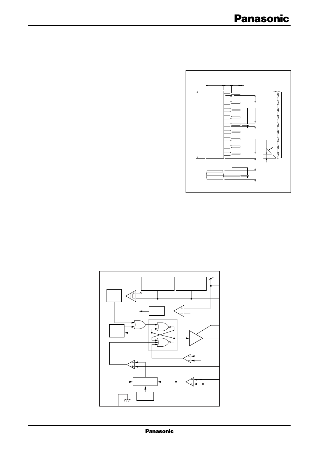
Voltage Regulators
AN8031
Active filter control IC
■ Overview
In supplying electric power from commercial power
6.0±0.3
2.4±0.25
3.3±0.25
Unit: mm
supply to various electrical equipment, there is a possibility that the harmonic distortion generated in the power
line may give obstruction to the power facilities or other
electrical equipment. The use of active filter is one of the
methods to solve the harmonic distortion problems.
The AN8031 is a monolithic IC which incorporates
the control and protection functions into one package so
that the active filter can be constructed easily. It is most
suitable for the measures against the harmonic distortion
problems such as lighting equipment.
■ Features
23.3±0.3
9
8
7
6
5
4
3
2
1
0.3
+0.1
–0.05
0.5±0.1
2.54
1.5±0.25
1.5±0.25
3.0±0.3
1.4±0.3
• Self-excited peak current mode is adapted.
• Built-in protection circuit for preventing the overvolt-
SIP009-P-0000C
age generated under a small load
• Easy constant setting with enlarged dynamic range of multiplier and error amplifier.
• Using totem pole output circuit which allows the power MOSFET to be directly driven.
• Built-in low voltage protection circuit which ensures the on-resistance during the power MOSFET operation.
• Timer circuit is built in for realizing automatic start.
■ Applications
• Lighting equipment and switching power supply equipment
30°
■ Block Diagram
MPI
3
One
shot
Timer
Current
comp.
7
2.5 V
GND
Under voltage
clamper
V
Multiplier
2.5 V
U.V.L.O. comp.
REF
Error amp.
4
Over voltage
clamper
10 V/8 V
Drive
OVP comp.
2.5 V
EO
2.6 V
1
SV
CC
6
V
B
9
PV
CC
8
V
OUT
2
CS
5
EI
1
Page 2

AN8031 Voltage Regulators
■ Pin Descriptions
Pin No. Symbol Description
1SVCCControl system supply-voltage pin
2 CS Comparator input pin
3 MPI Multiplier input pin
4 EO Error amplifier output pin / multiplier input pin
5 EI Error amplifier inverting input pin / overvoltage protection input pin
6VBTransformer-reset detection pin
7 GND Grounding pin
8V
OUT
9PVCCPower system supply-voltage pin
■ Absolute Maximum Ratings
Parameter Symbol Rating Unit
Supply voltage V
CS allowable application voltage V
MPI allowable application voltage V
EI allowable application voltage V
Output allowable current I
Peak output current I
VB allowable flow-in current I
VB allowable flow-out current I
Power dissipation P
Operating ambient temperature
Storage temperature
Note)*: Expect for the operating ambient temperature and storage temperature, all ratings are for Ta = 25°C.
*
Output pin
*
CC
CS
MPI
EI
O
OP
BI
BO
D
T
opr
T
stg
35 V
− 0.5 to +7V
− 0.5 to +7V
− 0.5 to +7V
±150 mA
±1A
+5mA
−5mA
874 mW
−30 to +85 °C
−55 to +150 °C
■ Recommended Operating Range
Parameter Symbol Range Unit
Supply voltage V
CC
■ Electrical Characteristics at Ta = 25°C
Parameter Symbol Conditions Min Typ Max Unit
Error detection feedback threshold V
voltage 1
Error detection low-level output voltage
Error detection high-level output voltage
Error detection input bias current I
Error detection output supply current I
2
EITH1
V
EOLIEO
V
EOHIEI
EI
EO
0 to 34 V
2.35 2.50 2.65 V
= 0 mA, VEI = 5 V 1.0 1.6 V
= 0 mA, VEI = 0 V 5.0 5 . 7 V
VEI = 0 V − 0.3 −1.0 µA
VEI = 0 V, VEO = 1 V 0.25 0.50 0.75 mA
Page 3

Voltage Regulators AN8031
■ Electrical Characteristics (continued) at Ta = 25°C
Parameter Symbol Conditions Min Typ Max Unit
Multiplier input D-range (upper limit) V
Multiplier output D-range (upper limit)
V
MPOHVEO
Multiplier gain G
Multiplier input bias current I
Coil detection input threshold voltage V
Coil detection hysteresis width dV
Coil detection high-level clamp voltage
Coil detection low-level clamp voltage
Current detection input offset voltage V
V
V
CSOFF
Current detection input bias current I
Overvoltage detection input V
threshold voltage
V
− V
OVP
EITH1
Low-level output voltage V
High-level output voltage V
Standby output voltage V
OUTLIOUT
OUTHIOUT
OUTSTBIOUT
U.V.L.O. start voltage V
U.V.L.O. stop voltage V
U.V.L.O. start - stop voltage difference
Standby current I
dV
CCSTBVCC
Operation current without load I
MPIHVEO
MP
MPI
BTH
B
BHIB
BLIB
CS
OVP
70 100 130 mV
CCST
CCSP
CC
CC
= 5 V 4.0 4.5 V
= 5 V 4.8 5.4 V
1.0 1.2 1.4 1/V
V
= 0 V −1.5 −3.0 µA
MPI
1.2 1.5 1.8 V
50 100 200 mV
= 5 mA 7.0 7.5 8.0 V
= −5 mA − 0.3 − 0.2 0 V
3.5 15 mV
VCS = 0 V − 0.5 −2.0 µA
2.45 2.60 2.75 V
= 100 mA 0.9 1.5 V
= −100 mA 9.2 10.2 V
= 10 mA 0.8 1.5 V
9.2 10.0 10.8 V
7.0 8.0 9.0 V
dVCC = V
CCST
− V
CCSP
1.75 2.00 2.50 V
= 7 V 40 80 120 µA
VCC = 12 V 6.0 10.0 mA
• Design reference data
Note) The characteristics listed below are reference values based on the IC design and are not guaranteed.
Parameter Symbol Conditions Min Typ Max Unit
Error detection feedback V
EITH2Ta
= −25°C to +85°C 2.3 2.7 V
threshold voltage 2
Error detection open-loop gain G
Error detection gain band width f
Multiplier input D-range (lower limit) V
Multiplier output D-range (lower limit)
Current detection − output delay td
Overvoltage detection − output delay td
Output rise time t
Output fall time t
Timer delay time td
AV
BW
MPILVEO
V
MPOLVEO
CS
OVP
r
f
TIM
= 5 V 0 V
= 5 V 0 V
VCC = 12 V, V
VCC = 12 V, V
= 10% → 90% 50 ns
OUT
= 90% → 10% 50 ns
OUT
85 dB
1.0 MHz
200 ns
500 ns
400 µs
3
Page 4
AN8031 Voltage Regulators
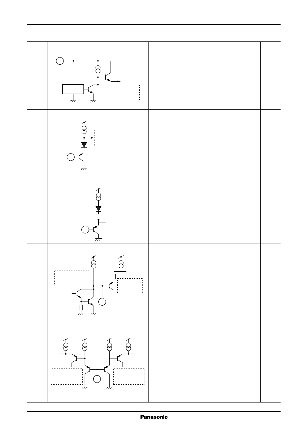
■ Terminal Equivalent Circuits
Pin No. Equivalent circuit Description I/O
1SV
1
:I
CC
The supply voltage terminal for control system.
It monitors the supply voltage and has operating
threshold value for start/stop.
U.V.L.O.
Internal bias
(Approx. 7.1 V)
2 CS: I
Approx. 7.1 V
The input terminal of comparator which detects
To high-speed
converter
the current value flowing in power MOSFET.
The output level of multiplier and the current
value of power MOSFET input from the CS
2
terminal are compared. If the later becomes larger
than the former, the V
is set to low level and
OUT
the power MOSFET output is cut.
3 MPI: I
Approx. 7.1 V
The input terminal of multiplier
The voltage after a full-wave rectified AC input
voltage are monitored.
3
4 EO: O
Approx. 7.1 V Approx. 7.1 V
The output terminal of error amplifier / the input
terminal of multiplier.
Error amplifier
output
Multiplier
input
4
The error amplifier monitors the output voltage
of active filter and amplifies its error portion and
outputs to the multiplier. Therefore, this terminal
serves as another input terminal of the multiplier.
5 EI: I
Approx.
7.1 V
Approx.
7.1 V
Approx.
7.1 V
Approx.
7.1 V
The inverted input terminal of error amplifier / the
overvoltage protection input terminal.
To the noninverted input terminal, the internal
reference voltage of IC (2.5 V typ.) is input.
Since this terminal monitors the output voltage of
Overvoltage
protection input
Error amplifier
5
output
the active filter, it also functions as the input terminal for the overvoltage protector which detects
the overvoltage of output voltage and cuts off the
power MOSFET.
4
Page 5
Voltage Regulators AN8031
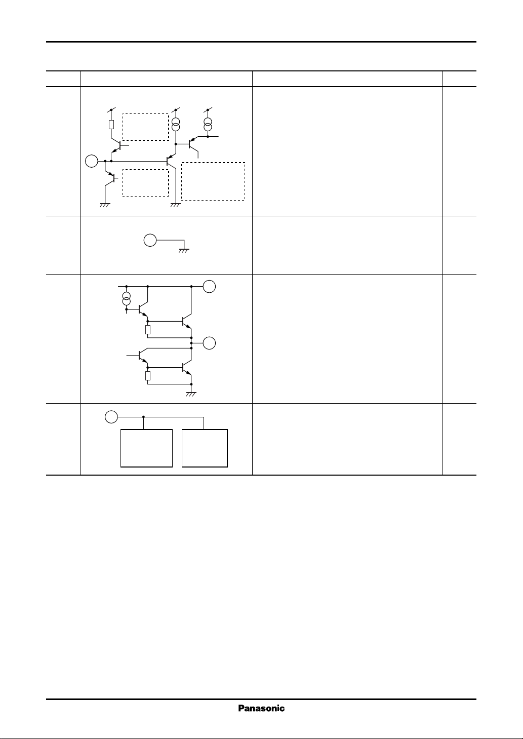
■ Terminal Equivalent Circuits (continued)
Pin No. Equivalent circuit Description I/O
6V
CC
Upper limit
voltage clamp
Approx. 7.1 VPV
Approx. 7.1 V
:I
B
The terminal is connected via the transformer's
sub-coil and resistor. The reset of transformer is
detected and the trigger signal to turn on the power
MOSFET is sent.
6
V
Lower limit
voltage clamp
B
Comparator
input
Since the coil signal of transformer is input as
current, the IC incorporates the circuit which
clamps the upper/lower limit voltage to prevent
malfunction.
7 GND:
7
Grounding terminal
This terminal is used in common for grounding
the control system and the power system.
8V
9
:O
OUT
The output terminal.
It is capable of driving the gate of power MOSFET
directly.
8
9 PV
9
:
CC
The supply voltage terminal for power.
V
B
upper limit
voltage clamp
Power
MOSFET
drive block
It determines the upper limit of output drive voltage. Normally, it is used at the same potential of
SVCC .
5
Page 6
AN8031 Voltage Regulators
■ Application Notes
[1] PD Ta curve of SIP009-P-0000C
1 000
900
874
800
700
(mW)
D
600
500
400
Power dissipation P
300
200
100
0
0 25 150
[2] Operation descriptions
1. Normal control
1) Application outline
As shown in figure 1, the standard application of the AN8031 is a booster chopper circuit, which inputs
the voltage rectified from the commercial supply of 100 V/200 V (A in figure 1) and outputs the DC voltage
of 400 V (B in figure 1).
It controls so that the input current proportional to the input voltage (C, D in figure 1) could be flown.
The reason for selecting the output voltage of 400 V is that the withstanding voltage of components and
the operation limitation of booster chopper (input voltage < output voltage) under the worldwide input
voltage are taken into consideration.
PD T
a
Independent IC without a heat sink
R
= 143°C/W
th( j−a)
PD = 874 mW (25°C)
50 75 10085 125
Ambient temperature Ta (°C)
Booster circuit so that set at: E
IN(max)
< E
OUT
D. Input current
0 A
(IIN)
A. Voltage after rectification
)
(E
IN
E
IN(max)
0 V
B. Output voltage (E
400 VDC
0 V
OUT
)
Active filter
Input current proportional
I
IN
E
IN
E
OUT
Output
to input voltage flows.
SBD
C. Input voltage (VIN)
Commercial
power supply (AC)
Input
Load
V
IN
Diode bridge
AN8031
0 V
Booster chopper circuit
Figure 1. Application outline description
6
Page 7
Voltage Regulators AN8031
■ Application Notes (continued)
[2] Operation descriptions (continued)
1. Normal control (continued)
2) Control outline description (Refer to figure 2 and figure 3.)
(1) Input voltage (E
The voltage which is divided from the input voltage of chopper circuit (E
resistor is input to the multiplier input terminal of the AN8031 (MPI terminal).
(2) Output voltage (E
The voltage which is divided from the output voltage of chopper circuit (E
resistor is amplified by the error amplifier of the AN8031 (Input to inverted input terminal (EI terminal))
and input to another multiplier input (EO terminal, which also functions as output for error amplifier).
(3) Multiplication of input voltage and output voltage
The signals input to the multiplier are multiplied and outputted from the multiplier. This output is a
signal which monitors both the input voltage and output voltage of the chopper circuit.
MPI
input voltage
0 V
) detection
IN
) detection
OUT
) by using the external
IN
) by using the external
OUT
Time
EI
input voltage
Multiplier output
(MPO) voltage
Transformer reset
voltage detection (V
Approx. 2.5 V typ.
0 V
0 V
0 V
)
B
0 V
Enlarged
Power MOS turned off
Power MOS turned off
Time
Time
Multiplier output (MPO) voltage
Power MOSFET current detection
(CS) voltage
Time
V
lower limit voltage (regulated inside IC)
B
Power MOS turned on = bias coil voltage
generated
Reset operation of transformer = bias coil
voltage inversion
VB lower limit voltage (regulated inside IC)
Time
Figure 2. Explanation of normal control operation
7
Page 8

AN8031 Voltage Regulators
■ Application Notes (continued)
[2] Operation descriptions (continued)
1. Normal control (continued)
2) Control outline description (Refer to figure 2 and figure 3.) (continued)
(4) Switching device current
The voltage generated in the current detection resistor which is connected to the switching device
(power MOSFET) is detected at the CS terminal. (for the above resistor, low resistance value is selected,
considering the power dissipation).
(5) Switching device turn-off
The CS terminal voltage and the multiplier output voltage are compared by the current detection
comparator. When the former value becomes larger than the latter one, the current detection comparator
sends the reset signal to the RS latch circuit to turn off the switching device.
(6) Output current supply
When the switching device is turned off, the current flowing in the transformer is cut off. The diode
is turned-on with inertia current of inductor, and supplies a current to the output of chopper circuit
(E
).
E
IN
OUT
One shot
Power MOS
SV
1
BTH
Lower limit
voltage clamp
V
Upper limit
voltage clamp
CC
V
6
B
→ On
Power MOS
→ Off
Input voltage
monitor
Turn-on signal
2.5 V
Timer
V
REF
Latch circuit
10 V/8 V
Low voltage
protection
Drive
PV
9
CC
V
8
OUT
Power MOSFET
SBD
2.6 V
Turn-off signal
MPI
Current detection
comparator
3
Multiplier
Overvoltage detection
Error amp.
2
CS
5
EI
2.5 V
7
GND
2.5 V
4
EO
Current detection
resistor
Figure 3. Explanation of block diagram and normal operation
(7) Transformer reset signal (VB) detection
When the excitation energy has been discharged and the inertia current of the inductor has been lost,
the transformer starts resonance with the frequency which depends on parasitic capacitance of the board
or parts and inductance of the inductor. This operation is detected at the V
terminal through sub-coil of
B
the transformer.
E
OUT
8
Page 9

Voltage Regulators AN8031
■ Application Notes (continued)
[2] Operation descriptions (continued)
1. Normal control (continued)
2) Control outline description (Refer to figure 2 and figure 3.) (continued)
(8) Switching device turn-on
By resonance, the turn-on signal is sent to the switching device, timed with the sub-coil voltage when
it swings from high to low.
(9) Continuation of operation
When the switching device is turned on, current flows in the inductor so that the above operation is
repeated.
<Summary>
• When the excitation energy of inductor is lost and the free resonance is started, the switching device turns on.
• The switching device will turn off when the following two elements cross each other: The product of the input
voltage (E
• The fluctuation of input voltage and load current is controlled by changing the peak value height of switching
device current.
• The purposes of mixing two signals by using the multiplier are:
3) Description of each function
(1) V
• Function
MOSFET at the next cycle.
• Method
It is difficult from the view point of withstanding voltage to input this voltage directly to the IC. For this
reason, it is input to the V
• Function of upper limit voltage clamper
• Function of lower limit voltage clamper
case of monolithic IC, malfunction (such as latch-up) occurs when the terminal voltage decreases to a value
below −V
• IC inside
V
tion, this function precedes the former.
) and output one (E
IN
) of the chopper circuit, and the switching device current.
OUT
to stabilize the control system
to reduce the number of components required
B
It detects the discharge of the excitation energy of the inductor (reset operation) and turns on the power
When the inductor is reset, the sub-coil provided on the inductor (bias winding) starts free resonance.
terminal through resistor.
B
It prevents the damage when the VB terminal voltage exceeds the withstanding voltage.
It prevents the malfunction when the V
and the parasitic device is activated.
BE
terminal voltage swings to negative voltage: generally, in the
B
The VB terminal voltage is input to the comparator with hysteresis inside the IC. For this reason, if the
terminal voltage is under the threshold value, the power MOSFET is turned on.
B
However, if the off signal has been given to the power MOSFET by the overvoltage protection func-
Power MOSFET
terminal input voltage
V
B
V
BTH
(1.5 V typ.)
OFF ON OFF
0 V
Figure 4. VB terminal description
9
Page 10

AN8031 Voltage Regulators
■ Application Notes (continued)
[2] Operation descriptions (continued)
1. Normal control (continued)
3) Description of each function (continued)
(continued)
(1) V
VB lower limit
voltage clamp
current
VB upper limit
voltage clamp
current
AN8031
Lower limit
voltage clamp
B
V
CC
V
B
V
B
I
D
SDB
I
DS
I
DS
Clamp upper
limit voltage
V
B
I
D
V
B
threshold value
Time
Upper limit
voltage clamp
GND
Figure 5. Explanation of V
<Setting the VB terminal constant>
• Regulation by clamper in/out-current value
The allowable output current of the upper
limit voltage clamper is −5 mA and the allowable input current of the lower limit voltage
clamper is +5 mA.
Either one of these allowable values is exceeded, the voltage clamp operation of the V
terminal is not guaranteed. Therefore, RB should
be set so that these values are not exceeded.
• Consumption current and delay
When the R
value is too large, the V
B
threshold could be exceeded. When the RB value
is too small, the consumption current becomes
too large.
In order to determine the R
value prop-
B
erly, the input voltage range and the dispersion
of components should be taken into consideration and it should be confirmed that a stable
operation can be ensured under start/overload
conditions or under a small load condition.
Clamp upper
limit voltage
operation
B
Reset operation
of inductor
±5 mA or less
AN8031
V
B
R
B
B
RB too large: Consumption current becomes small, however,
B
T
is extended by the delay amount because of low speed.
OFF
RB too small: Speed is high, however, consumption current
is small and undershoot tends to be generated easily.
Time
10
Page 11

Voltage Regulators AN8031
■ Application Notes (continued)
[2] Operation descriptions (continued)
1. Normal control (continued)
3) Description of each function (continued)
(continued)
(1) V
B
<Setting the V
terminal constant> (continued)
B
• Zero-cross switching
Zero-cross switching can be realized by using
the local resonance when turning off the power
MOSFET in order to suppress the loss.
By connecting the resonance capacitor C
tween the drain and source of the power MOSFET,
and using the inductance of the transformer's primary side L
, the resonance is produced after dis-
P
charging the accumulated energy of the transformer.
The capacitor for delay should be connected to the
V
terminal so that the next turn-on could occur at
B
the time when the resonance occurred and the drain
voltage of the power MOSFET has reached around
0 V.
However, it is necessary to take care that the
zero-cross conditions could deviate since the delay
amount varies depending on the conditions such as
the input voltage.
(2) CS
The terminal for detecting the current when the power MOSFET is turned on.
The current flow when the power MOSFET is turned on is equivalent to the current flow in the
inductor. Therefore, the necessary power value can be controlled by controlling the peak value of the
above current.
The input D-range of this terminal is from 0 V to 5 V. However, since dissipation becomes larger if
the power MOSFET current detecting resistance is set at larger value. A value from 0.22 Ω to 0.47 Ω is
the standard considering the relationship with the S/N.
The charge and discharge current to and from the parasitic capacitance of the power MOSFET,
transformer or printed circuit wiring flow in the power MOSFET detection resistor at turning-on and off.
Since such current generates noise and causes malfunction, it is necessary to incorporate a filter to remove such irregular element.
be-
P
AN8031
V
A-point voltage
0 V
B-point voltage
0 V
Delay capacitor
A
V
B
OUT
V
BTH
Power MOSFET Power MOSFET
B
C
B
Resonance capacitor
Resonance by LP − C
Delay
R
B
C
P
Zero-cross
switching
On Off
L
P
P
V
B
Parasitic
capacitance
Filter
I
CS
0 A
Spike
Spike
Figure 6. CS terminal explanation
(3) MPI
The MPI is the terminal for monitoring the AC input voltage. The voltage which is resistance-divided
input voltage after full-wave rectification is input. The input D-range of the multiplier is from 0 V to 4.5
V typical and output D-range is from 0 V to 5.4 V typical.
11
Page 12

AN8031 Voltage Regulators
■ Application Notes (continued)
[2] Operation descriptions (continued)
1. Normal control (continued)
3) Description of each function (continued)
(4) EI/EO
The resisitance-devided voltage of the active filter output is input to the EI. The EI is the error
amplifier's inverted input, and the temperature-compensated reference voltage (2.5 V typical) is input as
the noninverted input. The error amplifier amplifies the error amount between the output voltage, and the
reference voltage and outputs to the multiplier. The resistor between the EI and EO is used for determining the gain of error amplifier.
As for the resistance-dividing for decreasing the active filter's output voltage to the input D-range of
EI, if an attempt is made to use a small-sized resistor for suppressing the dissipation, its resistance value
becomes high because of the high output voltage. For this reason, note that if the capacitance inserted
between the EI and EO for phase compensation is large, the delay element between it and the resistancedivider of high resistance becomes large, so that the characteristics at the time of sudden change of load
(overshoot or undershoot) is degraded.
Therefore, as the value for phase compensation capacitor, select the minimum value with which the
oscillation can be prevented.
Output
To multiplier
Error amplifier
4
Reference voltage
(2.5 V typ.)
EI
5
SBD
EO
(5) V
Resistor determining the gain
Figure 7. EI/EO terminal description
OUT
Phase compensation capacitor
For the drive circuit, the AN8031 employs the totem pole type by which the power MOSFET can be
directly driven. Since the peak output current is ±1 A, the TO-220 class power MOSFET can be driven.
For the TOP-3 class, the buffer circuit should be added outside because its capability is not sufficient for
that class.
The power MOSFET momentarily swings to minus due to the parasitic capacitance between the
drain and gates at the time of turn-off and this causes malfunction in some cases. Therefore, the Schottky
barrier diode should be inserted between the V
PV
CC
and GND if necessary.
OUT
Power
MOSFET
V
D
Off On
Parasitic
capacitance
0 V
Capacitive coupling
V
G
output circuit
Totem pole type
V
OUT
V
G
V
D
GND
0 V
12
Figure 8. V
terminal description
OUT
Swing to negative voltage
Page 13

Voltage Regulators AN8031
■ Application Notes (continued)
[2] Operation descriptions (continued)
1. Normal control (continued)
3) Description of each function (continued)
(6) V
CC
The supply voltage terminal other than the
output. The U.V.L.O. depends on this V
(The characteristics of U.V.L.O. are shown in the
right figure.)
voltage.
CC
I
CC
U.V.L.O.
characteristics
0810
(Stop voltage) (Start voltage)
IC operation
V
V
CC
<Note on the methods of providing V
CC
>
• The method to give bias from sub-coil
There is only 2 V typical difference between the
start voltage 10 V typical and the stop voltage 8 V
typical. Be careful that the value for C1 shown in the
right figure must be set at a large value, otherwise,
the IC does not easily start.
• Giving bias from power supply
In the case such as of fluorescent lamp inverter
circuit, separate power supply is provided so as to
give the bias from the separate power supply.
(7) PV
CC
Drive current supply terminal of output block
The high voltage of the power MOSFET gate
drive pulse is determined by this terminal voltage.
In the case of limiting the power MOSFET
drive current, if the R1 is connected to the PV
terminal and the R2 is connected to the V
minal as shown in the right figure, the R1 + R2
limits the drive current when the power MOSFET
is turned on and the R2 limits the drive current
when it is turned off. In that way, the speed of turnon and turn-off can be changed.
OUT
CC
ter-
Start resistance
R1
V
V
CC
OUT
C1
AN8031
GND
V
CC
AN8031
C1
GND
Totem pole type output circuit
PV
CC
Drive current
at turning on
V
OUT
Drive current
at turning off
GND
To fluorescent lamp
inverter circuit block
R1
R2
13
Page 14

AN8031 Voltage Regulators
■ Application Notes (continued)
[2] Operation descriptions (continued)
2. Protection circuit
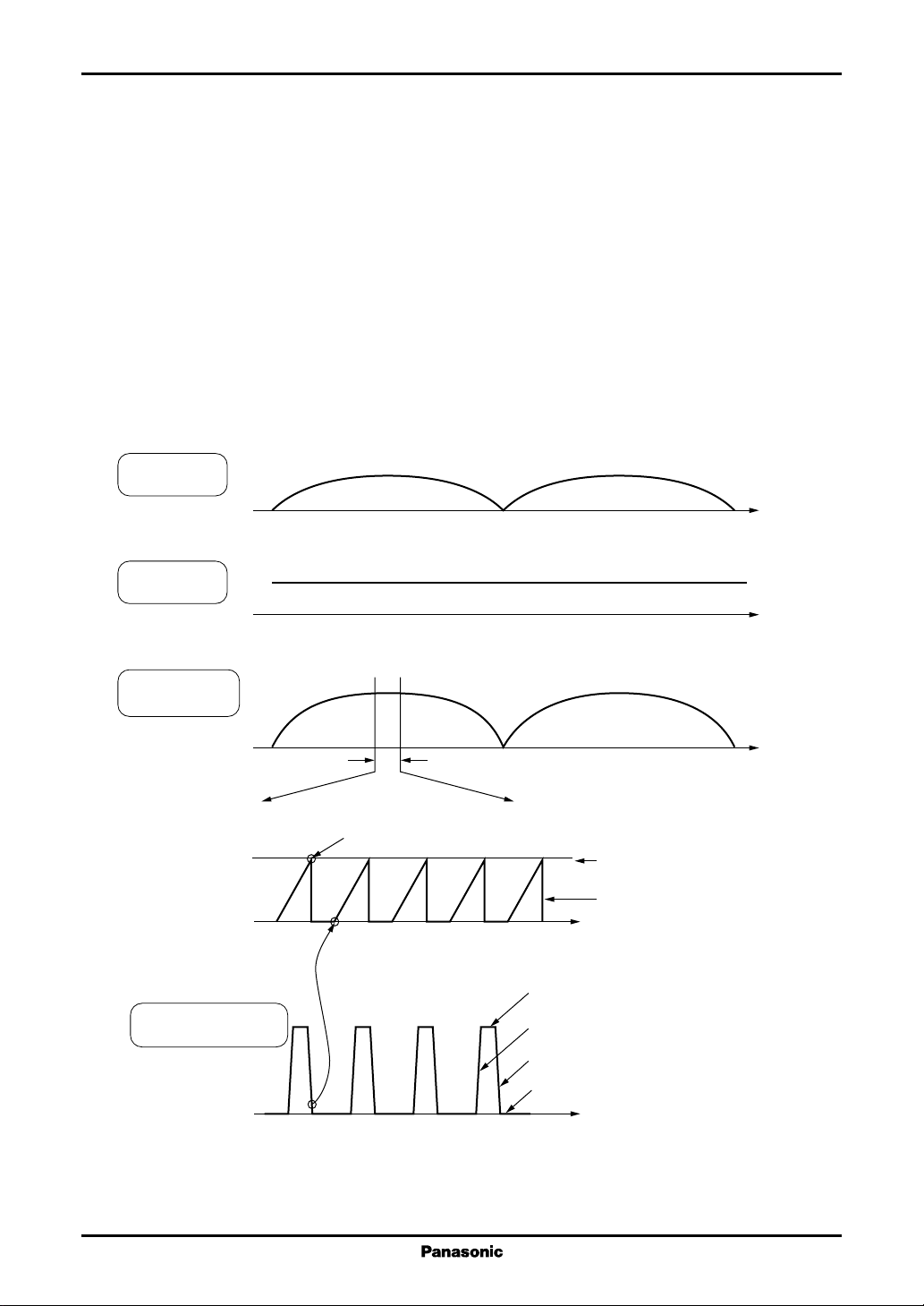
1) Timer
In control of this IC, the chopper circuit does not start unless the first on-signal is input to the switching
device. The chopper circuit does not re-start, if the turn-on timing of switching device is missed due to some
abnormality.
For the above reasons, this IC is incorporating the timer circuit and generating the start pulse once in
every approx. 400 µs (typical) when the chopper circuit stops, eliminating the need for an external part to cope
with this problem. (Refer to figure 9.) However, in order to prevent the output rise of the chopper circuit, the
timer circuit does not operate as long as the overvoltage protector is operating.
When operation start
Timer trigger
signal (signal
inside the IC)
Input voltage
Power MOSFET current
When abnormal stop
Timer trigger
signal (signal
inside the IC)
Input voltage
Input voltage applied
operation start
0 A
400 µs typ.
0 V
0 A
One-shot pulse
Start
400 µs typ.
Time
Time
One-shot pulseTimer start
Time
14
Power MOSFET current
0 V
Abnormal stop
Figure 9. Explanation of timer operation
Re-start
Time
Page 15

Voltage Regulators AN8031
■ Application Notes (continued)
[2] Operation descriptions (continued)
2. Protection circuit (continued)
2) Overvoltage protection
(1) Cause of overvoltage
In the booster chopper circuit, control is carried out so that the input power becomes zero when the
load current reaches zero. However, in the actual condition, the input power can not be decreased to zero.
The output voltage is brought to out of control state, so that it rises.
The cause of the out-of-control condition is that there is a delay time from the turn-on to the turn-off
of the switching device, so that the control to stop the operation of switching device becomes impossible.
(Refer to figure 10.)
In order to prevent the occurrence of such problem, the AN8031 has the built-in overvoltage protection circuit, so that the number of component to be added to the external part is drastically reduced.
Power MOS off-time current
Under light load
Multiplier output
Power MOS
on-time current
Power MOS
off-time current
Under light load
Multiplier output
Power MOS on-time current
Input voltage
Under no load condition, this voltage decreases to around 0 V.
At this time, the frequency of power MOS current rises,
however, there is circuit delay, so that the current does not reach 0 A.
0 A
AN8031
SBD
Output voltage
Time
Power MOS
on-time current
Power MOS
off-time current
0 A
Time
Figure 10. Explanation of operation
15
Page 16

AN8031 Voltage Regulators
■ Application Notes (continued)
[2] Operation descriptions (continued)
2. Protection circuit (continued)
2) Overvoltage protection (continued)
(2) Description of overvoltage protector operation
With respect to the AN3081 IC, the input of the error amplifier which detects the output voltage is also
commonly used as the input of the overvoltage protection comparator. This is the point which differs
from the AN8032.
Each setting is shown as follows:
• Control reference voltage of the error amplifier: 2.50 V typical
• Detection voltage of the overvoltage comparator: 2.63 V typical [Without hysteresis]
(Voltage of 5% higher than the control reference voltage of the error amplifier)
If the output voltage becomes more than 5% higher than the normal control voltage at the time of
start up or abnormality occurrence, the overvoltage comparator operates to cut off the switching device.
The timer circuit is cut off when overvoltage is detected. This prevents the output voltage to increase
further. Otherwise, the timer circuit will re-start the power MOSFET, and actuate it to increase the output
voltage further at the time of the overvoltage detection.
Therefore, under no load condition, the output voltage of the chopper circuit is stabilized at the value
which is 5% higher than the normal control voltage and does not exceed that value. (Refer to figure 11.)
The increase/decrease of the output voltage is created by the offset amount of the overvoltage comparator.
Output voltage of
active filter
Power MOSFET current
Operation condition
of active filter
420 V
400 V
Stabilized at 5% higher voltage
0 A
Operating
Figure 11. Protection of overvoltage protection operation
Stop
Operating
Created by offset amount
of overvoltage comparator
Time
Stop
16
Page 17

Voltage Regulators AN8031
■ Application Notes (continued)
[2] Operation descriptions (continued)
2. Protection circuit (continued)
2) Overvoltage protection (continued)
(3) Output voltage overshoot at start
At operation start, the output overload condition is created because the smoothing capacitor which is
connected to the output is charged. Under this condition the chopper circuit operates with full power.
However, it does not immediately come out of the full-power-operation due to control delay even when
the proper output voltage is obtained, causing the overshoot of output voltage.
The AN8031 overvoltage protector operates even at operation starts and prevents the worst cases
such as damage of used parts.(Refer to figure 12.)
Overvoltage protector operation
Operation start
Overvoltage
condition
Set output voltage
Output voltage of
active filter
0 A
Power MOSFET current
0 A
Operation condition of
active filter
Time
Start under output
short-circuit condition →
Current peak value is high
Time
Stop OperatingOperating
Figure 12. Output voltage overshoot when operation starts
17
Page 18

AN8031 Voltage Regulators
■ Application Notes (continued)
[3] Difference between the AN8031 and the AN 8032
AN8031 → EI terminal is used in common for both the output voltage monitor function and the overvoltage
detection function.
AN8032 → Exclusive-use terminal for each function (V
EI terminal : Exclusively used for the output voltage monitor function.
OVP terminal: Exclusively used for the overvoltage detection function.
1) Reasons for change
The excessively large overvoltage, generated when the short-circuit test between the pins of the active filter
output voltage monitoring resistor, can not be suppressed.
terminal is used in common for both PVCC and VCC).
CC
E
SBD
O(+)
E
IN(+)
E
IN(−)
2) Countermeasures
The output voltage system and the overvoltage detection system are separated from each other.
E
IN(+)
E
IN(−)
MPI
MPI
B
PVCCV
V
Output voltage
monitor
Overvoltage
detection
AN8031
COM
B
V
Output voltage
monitor
AN8032
Overvoltage
detection
COM
CC
V
OUT
EI
EO
CS
SBD
CC
V
V
OUT
EI
EO
OVP
CS
Separately require
5 to 10 external
components
Excessively large
overvoltage,
generated when the
short circuit testing,
can not be suppressed.
E
O(−)
E
O(+)
Increase of 2 more
external components
The control operation
is stopped by the
separately provided
circuit for overvoltage
system
even if excessively
large overvoltage is
generated.
E
O(−)
18
Note) The OVP terminal is arranged beside the EI terminal after taking the board pattern design into consideration.
Page 19

Voltage Regulators AN8031
■ Application Circuit Example
• Application circuit
G
R8
1.5 MΩ
EO(DC 400 V)
C3
47 µF
SBD
Load
R7
COM
R9
10 kΩ
330 Ω
R6
0.33 Ω
1 W
SBD
R4
12 Ω
CC
12 V
V
D
V
PV
OUT
CC
F
E
CS
2
8
EI
5
R10
C7
EO4
10 MΩ
0.1 µF
C6
0.001 µF
9
SV
L2
CC
1
C
GND7
R3
10 kΩ
V
6
B
3
C5
A
R1
B
1 MΩ
MPI
C4
0.01 µF
10 µF
R2
13 kΩ
EI
+
C2
1 µF
COM
−
L1
C1
19
Page 20

AN8031 Voltage Regulators
■ Application Circuit Example (continued)
• Normal operation waveforms
Horizontal axis
Measuring point
1 ms/div 10 ms/div
A
(EIN)
B
(MPI)
C
(VB)
D
(V
OUT
140 V
20 V/div
0 V
2 V
0.4 V/div
0 V
7 V
1 V/div
0 V
12 V
)
2 V/div
0 V
140 V
20 V/div
0 V
7 V
1 V/div
0 V
12 V
2 V/div
0 V
20
E
(CS)
F
(EI)
G
(EO)
0.8 V
0.2 V/div
0 V
2.5 V
0.5 V/div
0 V
500 V
50 V/div
100 V
0.8 V
0.2 V/div
0 V
2.5 V
0.5 V/div
0 V
Page 21

Voltage Regulators AN8031
■ Application Circuit Example (continued)
• Waveforms at start
Horizontal axis
Measuring point
1.2 V
E
(CS)
0.2 V/div
0 V
400 V
G
(EOI)
50 V/div
100 V
• Waveforms at stop
Horizontal axis
Measuring point
20 ms/div
20 ms/div
E
0.8 V
(CS)
0.2 V/div
0 V
400 V
G
(EOI)
50 V/div
100 V
(Conditions)
•Input voltage : 100 V (AC)
•Output voltage: 400 V (DC)
•Output current : 200 mA (resistive load 2 kΩ)
21
 Loading...