

Page 1
Voltage Regulators
AN8022L, AN8022SB
AC-DC switching power supply control IC
■ Overview
The AN8022L and AN8022SB are ICs which are
suitable for controlling a switching power supply using
primary side control method.
Those are most suited for a switching power supply
of relatively small capacity. Less frequently used functions are removed, and only the necessary minimum functions are incorporated, so that they are compact and very
easy to use.
Moreover, the internal settings are incorporated as
much as possible, thus cost down can be realized by decreasing the peripheral parts.
■ Features
•
It operates at a control frequency up to 700 kHz, realizing the output rise time of 35 ns and the output fall time
of 25 ns.
•
Pre-start operating current is as small as 70 µA (typical)
so that it is possible to miniaturize the start resistor.
•
Output block employs totem pole method.
The absolute maximum rating of ±1.0 A (peak) allows
the direct drive of power MOSFET.
•
Built-in pulse-by-pulse overcurrent protection circuit
•
Built-in protection circuit against malfunction at low
voltage (on/off: 14.2 V/9.2 V)
•
Maximum Duty is 44% (typical)
•
Equipped with timer latch function and overvoltage protection circuit.
•
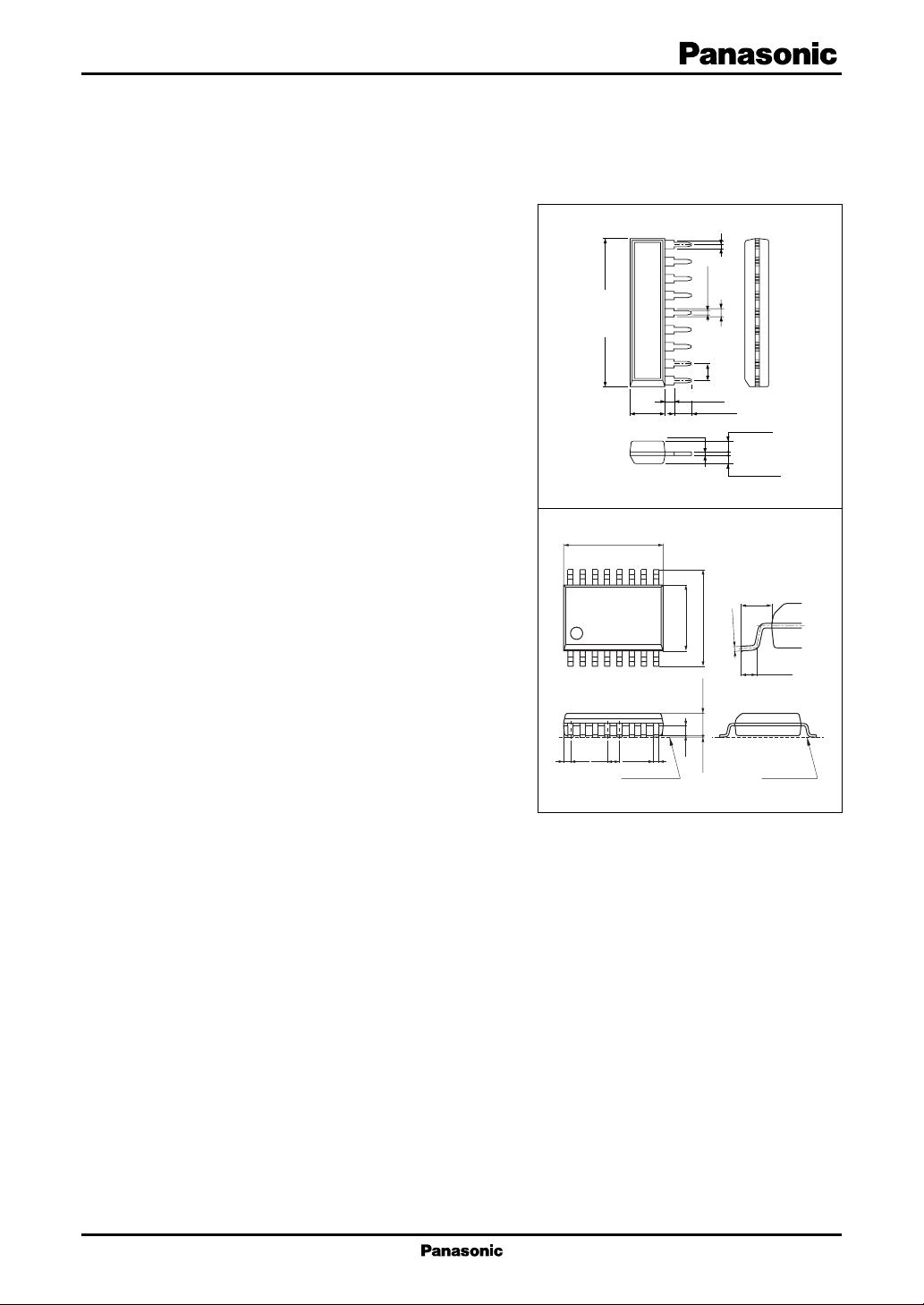
Two kinds of packages: 9-pin SIP, 16-pin SOP
AN8022L
21.7±0.3
4.3±0.3
1.0±0.25
0.3
9
8
7
6
5
4
3
2
1
2.7±0.25
+0.1
–0.05
0.5±0.1
Unit: mm
0.4±0.25
1.2±0.25
2.54
1.4±0.25
1.35±0.25
SIP009-P-0000D
AN8022SB Unit: mm
6.50
±0.30
16
1
(0.45)
0.80
9
±0.30
±0.30
6.30
4.30
8
±0.20
1.50
±0.10
±0.10
0.65
0.10
0.35
Seating plane
SSOP016-P-0225B
0
5
.1
.0
0
-0
+
0.15
1.00
±0.20
0.50
±0.05
Seatng plane
■ Applications
•
Various power supply equipment
1
Page 2
AN8022L, AN8022SB Voltage Regulators
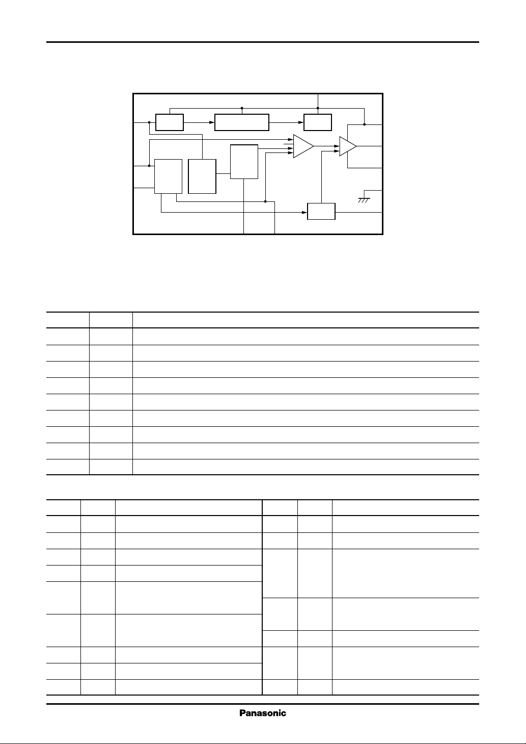
■ Block Diagram
CC
(4)SV
TIM/OVP
8
OVP
Start/Stop
(5)
4.1 V
CT
(13)
RT
3
2
OSC OCL
FB
(12)
9
(6)
IFB
Note) The number in ( ) shows the pin number for the AN8022SB.
1
Reset
SS
(11)
PWM
V
REF
CLM
Drive
7
V
CC
(3)PV
6
V
OUT
(2)
5
GND
(1)PGND
(16)SGND
4
CLM(−)
(15)
CC
■ Pin Descriptions
•
AN8022L
Pin No. Symbol Description
1 SS Soft start pin
2 RT Resistor connection pin that determines charge and discharge current of triangular wave
3 CT Triangular wave generating capacitor connection pin
4 CLM(−) Pulse-by-pulse overcurrent protection input pin
5 GND Grounding pin
6V
OUT
7VCCPower supply voltage pin
8 TIM/OVP Pin for overvoltage protection and timer latch (joint use)
9 IFB Current feedback signal input pin from power-supply-output photocoupler
Power MOSFET direct drive pin
•
AN8022SB
Pin No. Symbol Description
1 PGND Grounding pin
2V
Power MOSFET direct drive pin
OUT
3PVCCPower supply voltage pin
4SVCCPower supply voltage pin
5
TIM/OVP
Pin for overvoltage protection and
timer latch combined use
6 IFB Power supply output photocoupler
current feedback signal input pin
7 N.C. N.C.
8 N.C. N.C.
9 N.C. N.C.
2
Pin No. Symbol Description
10 N.C. N.C.
11 SS Soft start pin
12 RT Charge and discharge current of
triangular wave determining resistance
connection pin
13 CT Triangular wave generating capacitance
connection pin
14 N.C. N.C.
15 CLM(−) Pulse-by-pulse overcurrent protection
input pin
16 SGND Grounding pin
Page 3

Voltage Regulators AN8022L, AN8022SB
■ Absolute Maximum Ratings
Parameter Symbol Rating Unit
Supply voltage V
OVP terminal allowable application voltage V
CLM terminal allowable application voltage V
SS terminal allowable application voltage V
Constant output current I
Peak output current I
IFB terminal allowable application voltage I
Power dissipation AN8022L P
CC
OVP
CLM
SS
O
OP
FB
D
AN8022SB 340
Operating ambient temperature
Storage temperature
Note)*: Expect for the operating ambient temperature and storage temperature, all ratings are for Ta = 25°C.
*
*
T
opr
T
stg
■ Recommended Operating Range
Parameter Symbol Range Unit
Timing resistor R
T
R
7
35 V
V
CC
V
− 0.3 to +7.0 V
− 0.3 to +7.0 V
±150 mA
±1 000 mA
−5mA
658 mW
−30 to +85 °C
−55 to +150 °C
15 to 20 kΩ
■ Electrical Characteristics at Ta = 25°C
Parameter Symbol Conditions Min Typ Max Unit
Start voltage V
Stop voltage V
Standby bias current I
Operating bias current I
OVP operating bias current 1 I
OVP operating bias current 2 I
OVP operating threshold voltage V
OVP release supply voltage V
Timer latch charge current I
Timer latch start feedback current I
Soft-start charge current I
Overcurrent protection threshold voltage 1
Pre-start low-level output voltage V
Low-level output voltage V
High-level output voltage V
Oscillation frequency 1 f
Maximum duty 1 Du
Feedback current at 0% duty I
Feedback current at maximum duty I
CC-START
CC-STOP
CC-STB
CC-OPR
CC-OVP1VCC
CC-OVP2VCC
TH-OVPVCC
CC-OVPC
CH-TIM
FB-TIM
CH-SS
V
TH-CLM1VCC
OL-STBVCC
OL
OH
OSC1
max1
FB-Du
FB-Du
13.0 14.2 15.4 V
8.5 9.2 9.9 V
VCC = 12 V 50 7 0 105 µA
VCC = 34 V 6.4 8.0 9.6 mA
= 20 V 2.4 3.0 3.6 mA
= 10 V 0.44 0.55 0.66 mA
= 18 V 5.4 6.0 6.6 V
7.6 8.4 9.2 V
VCC = 18 V, RT = 19 kΩ−20 −30 −40 µA
VCC = 18 V − 0.32 − 0.44 − 0.56 mA
VCC = 18 V, RT = 19 kΩ−20 −30 −40 µA
= 18 V −180 −200 −220 mV
= 12 V, IO = 10 mA 0.8 1.8 V
VCC = 18 V, IO = 100 mA 1.3 1.8 V
VCC = 18 V, IO = −100 mA 15.0 16.5 V
VCC = 18 V 175 200 225 kHz
VCC = 18 V 40 4 4 48 %
VCC = 18 V − 0.9 −1.2 −1.5 mA
min
VCC = 18 V − 0.45 − 0.6 − 0.75 mA
max
3
Page 4
AN8022L, AN8022SB Voltage Regulators
■ Electrical Characteristics at Ta = 25°C (continued)
• Design reference data
Note) The characteristics listed below are theoretical values based on the IC design and are not guaranteed.
Parameter Symbol Conditions Min Typ Max Unit
Oscillation frequency 2 f
Overcurrent protection delay time t
OSC2
Dry-CLMVCC
Output voltage rise time t
Output voltage fall time t
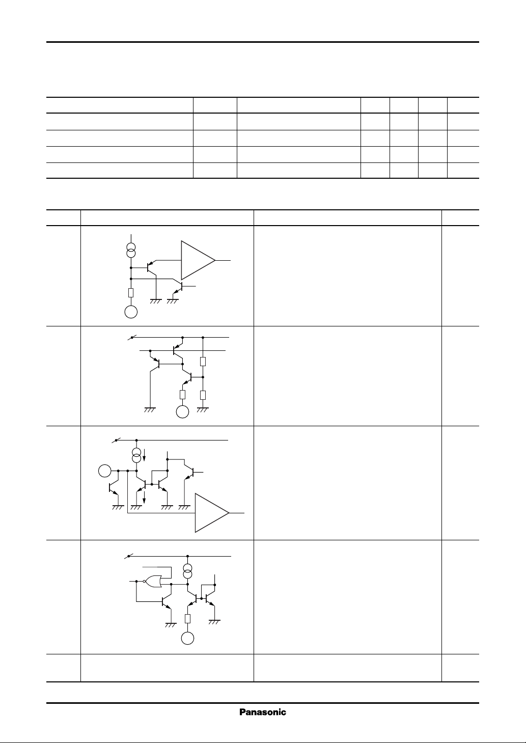
■ Terminal Equivalent Circuits
Pin No. Equivalent circuit Description I/O
1 SS:
(11) Soft start terminal.
500 Ω
1
(11)
PWM
comp.
Ta = −30°C to +85°C 160 240 kHz
= 18 V under no load 200 ns
VCC = 18 V under no load 35 ns
r
VCC = 18 V under no load 25 ns
f
When V
is applied, the capacitor connected to
CC
this pin is charged, and the output duty is decreased by inputting the capacitor voltage to the
PWM.
2 RT:
V
REF
(12) The terminal for connecting a resistor to deter-
mine the charge and discharge current of the
triangular wave.
500 Ω
2
(12)
3 CT:
V
(13) The terminal for connecting a capacitor to gener-
REF
(13)
I
O
ate the triangular wave.
3
2I
O
4 CLM(−): I
(15) The input terminal for pulse-by-pulse overcurrent
V
REF
Reset
PWM
comp.
protection. It is usually required to attach an external filter.
4
(15)
5 GND, (PGND), (SGND):
(1)(16) Grounding terminal.
Note) The number in ( ) is the pin number for the AN8022SB.
4
Page 5
Voltage Regulators AN8022L, AN8022SB
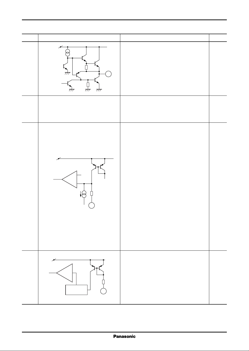
■ Terminal Equivalent Circuits (continued)
Pin No. Equivalent circuit Description I/O
6V
PV
CC
(2) The terminal for directly driving a power
6
(2)
7 VCC , (PVCC), (SVCC):
(3)(4) Supply voltage terminal.
8 TIM/OVP: I
(5) The terminal with double functions such as OVP
SV
CC
6 V
Comp.
5 µA
500 Ω
8
(5)
9 IFB: I
V
(6) The terminal into which the current feedback sig-
REF
PWM
comp.
500 Ω
I/V
conversion
9
(6)
:O
OUT
MOSFET.
It monitors the supply voltage and has operating
threshold value for start/stop/OVP reset.
(overcurrent protection) and timer latch terminal.
[OVP]
When it receives the overvoltage signal of the
power supply output and high is input to the
terminal, internal circuit is turned off. At the same
time, this condition (latch) is held. To reset the
OVP latch, it is necessary to reduce V
under the
CC
release voltage.
[Timer latch]
The output voltage drop due to the overcurrent
condition of power supply output is detected
through the current level of IFB-input. When I
FB
becomes less than a current of a certain value,
charge current flows into the capacitor connected
to this terminal. When the capacitor is charged to
the threshold voltage of OVP, OVP
starts to operate and the IC stays stop.
nal is input from the photocoupler of the power
supply output.
Note) The number in ( ) shows the pin number for the AN8022SB.
5
Page 6

AN8022L, AN8022SB Voltage Regulators
■ Application Notes
[1] Main characteristics [Load: CL = 3 300 pF, RL = 20 Ω]
Start/stop voltage characteristics OVP operation threshold voltage characteristics
VCC = 18 V
16
14
12
10
Start/stop voltage (V)
8
−50 −25 100
0 25 50 75
Ambient temperature (°C)
7.0
6.5
6.0
5.5
Threshold voltage (V)
5.0
−50 −25 100
0 25 50 75
Ambient temperature (°C)
Standby bias current characteristics Operating bias current characteristics
VCC = 12 V
75
70
65
60
Bias current (µA)
8.5
8.0
7.5
7.0
Bias current (mA)
VCC = 18 V
VCC = 34 V
55
−50 −25 100
0 25 50 75
Ambient temperature (°C)
6.5
−50 −25 100
0 25 50 75
Ambient temperature (°C)
Overcurrent protection threshold voltage characteristics OVP release voltage characteristics
−220
−210
−200
−190
Threshold voltage (mV)
−180
−50 −25 100
0 25 50 75
Ambient temperature (°C)
VCC = 18 V
9.5
9.0
8.5
8.0
OVP release voltage (V)
7.5
−50 −25 100
0 25 50 75
Ambient temperature (°C)
VCC = 18 V
6
Page 7

Voltage Regulators AN8022L, AN8022SB
■ Application Notes (continued)
[1] Main characteristics [Load: CL = 3 300 pF, RL = 20 Ω] (continued)
OVP operating bias current characteristics 1 OVP operating bias current characteristics 2
4.5
4.0
3.5
3.0
Bias current (mA)
2.5
-50 -25 100
0 25 50 75
Ambient temperature (°C)
VCC = 20 V
2.5
2.0
1.5
1.0
Bias current (mA)
0.5
-50 -25 100
0 25 50 75
Ambient temperature (°C)
VCC = 10 V
[2] Operation descriptions
1. Start/stop circuit block
• Start mechanism
When AC voltage is applied and the supply
voltage reaches the start voltage through the current from the start resistor, the IC starts operation. Then the power MOSFET driving starts.
Thereby, bias is generated in the transformer
and the supply voltage is given from the bias
coil to the IC. (This is point a in figure 1.)
During the period from the time when the
start voltage is reached and the voltage is gen-
After AC rectification
Start resistance
R1
V
CC
V
OUT
GND
C1
erated in the bias coil to the time when the IC is
provided with a sufficient supply voltage, the
supply voltage of the IC is supplied by the capacitor (C1) connected to V
CC
.
Since the supply voltage continuously decreases during the above period (area b in figure
1), the power supply is not able to start (state c
in figure 1), if the stop voltage of the IC is
Start voltage
Stop voltage
Before start Start
a
c
b
Figure 1
Voltage supplied
from bias coil
Start condition
Start failure
reached before the sufficient supply voltage is
supplied from the bias coil.
• Function
The start/stop circuit block is provided with the function to monitor the V
of IC when V
voltage reaches the start voltage (14.2 V typical), and to stop when it decreases under the stop
CC
voltage, and to start the operation
CC
voltage (9.2 V typical). A large voltage difference is set between start and stop (5.0 V typical), so that it is easier
to select the start resistor and the capacitor to be connected to V
Note) To start up the IC operation, the startup current which is a pre-start current plus a circuit drive current is necessary.
Set the resistance value so as to supply a startup current of 450 µA.
CC
.
7
Page 8

AN8022L, AN8022SB Voltage Regulators
■ Application Notes (continued)
[2] Operation descriptions (continued)
2. Oscillation circuit
The PWM is an abbreviation of Pulse Width Modulation. In this IC, a smaller voltage between the voltage level
which is converted from the current input to IFB terminal and dead-time control level which is fixed internally is
compared with the internal triangular oscillation level through PWM comparator, and optimal duty is determined,
and then it is output via output driving stage.
• Triangular wave oscillation
The triangular waveform oscillation is performed through constant current charge/constant current
discharge to/from the external capacitor connected to the CT. The ratio of the charge current to the discharge
current is set inside, and the current value is determined by the external resistor connected to the RT terminal.
The RT terminal voltage is determined by the level which is a resistor-divided voltage of the internal
reference voltage (which is determined by Zener diode and V
compensated). For this reason, the effect of fluctuation with temperature and dispersion is small. By the use
of a temperature-compensated external resistor, the effect of the fluctuation with temperature and dispersion
on the charge and discharge current value will be reduced further.
Moreover, since the upper/lower voltage level of the triangular wave oscillation is given by the resistordivider internal reference voltage, the effect of fluctuation with temperature and dispersion has been
suppressed.
Moreover, since the upper/lower voltage level of the triangular wave oscillation is given by the resistordivision of internal reference voltage, the effect of fluctuation with temperature and dispersion has been
suppressed.
As described above, the sufficient consideration has been given to the effect of fluctuation with
temperature and dispersion in the design of the triangular wave oscillation frequency.
(Reference calculation of oscillation frequency)
6 × C
5
T
× R
[Hz]
T
f
OSC
=
3. Overvoltage protection circuit (OVP)
OVP is an abbreviation of Over Voltage Protection. It refers to a self-diagnosis function, which stops the power
supply to protect the load when the power supply output generates abnormal voltage higher than the normal
output voltage due to failure of the control system or an abnormal voltage applied from the outside (figure 2 and
figure 3).
Basically, it is set to monitor the voltage of supply voltage V
CC
is supplied from the transformer drive coil. Since this voltage is proportional to the secondary side output voltage,
it still operates even when the secondary side output has over voltage.
1) When the voltage input to the OVP terminal exceeds the threshold voltage (6.0 V typical) as the result of power
supply output abnormality, the protective circuit shuts down the internal reference voltage of the IC to stop all
of the controls and keeps this stop condition.
2) The OVP is released (reset) under the following conditions:
• Decreasing the supply voltage (V
< 8.4 V typical: OVP release supply voltage)
CC
The discharge circuit is incorporated so that the electric charge which is charged in the capacitor
connected to the OVP terminal can be discharged with the constant current of 5 µA (typical) for the next re-start.
V
th(OUT)
V
7
= V
Secondary side output voltage under normal operation V
th(OVP)
V
th(OUT)
V
th(OVP)
V
Z
=
VCC terminal voltage under normal operation
+ V
Z
: Secondary side output overvoltage threshold
: OVP operation threshold
: Zener voltage (external parts of OVP terminal)
of NPN transistor, and temperature-
BE
terminal of the IC. Normally, the VCC voltage
OUT
× V
7
8
Page 9

Voltage Regulators AN8022L, AN8022SB
■ Application Notes (continued)
[2] Operation descriptions (continued)
3. Overvoltage protection circuit (OVP) (continued)
OVP
V
TIM/OVP terminal voltage
0 V
TH
(to 6 V)
Time
Internal reference voltage
Triangular wave oscillation
IC output
After AC rectification
Start resistor
V
CC
R1
0 V
0 V
0 V
(to 7.1 V)
(IC stop state)
(to 5 V)
(to 2 V)
(IC stop state)
(to VCC)
(IC stop state)
Figure 2. Explanation of OVP operation
Power supply output
FRD
Abnormal voltage applied from outside
Time
Time
Time
Load
V
GND
OVP
OUT
It detects abnormal voltage applied from the outside to the
power supply output (the voltage which is higher than voltage
of the power supply output and may damage the load) by the
primary side of the bias coil and operates the OVP.
Figure 3
•Operating supply current characteristics
While the OVP is operating, the decrease of the supply current causes the rise of the supply voltage VCC , and
in the worst case, the guaranteed breakdown voltage of the IC (35 V) can be exceeded. In order to prevent the rise
of supply voltage, the IC is provided with such characteristics as the supply current rises in the constant resistance
mode. This characteristics ensure that the OVP can not be released unless the AC input is cut, if the supply voltage
V
under OVP operation is stabilized over the OVP release supply voltage (which depends on start resistor
CC
selection). (Refer to figure 4.)
9
Page 10

AN8022L, AN8022SB Voltage Regulators
■ Application Notes (continued)
[2] Operation descriptions (continued)
3. Over voltage protection circuit (OVP) (continued)
The current supply from the start resistor continues
as long as the voltage of the power supply input (AC)
After AC rectification
Start resistor
V
CC
R1
is given.
After OVP starts operation, since the output is
stopped, this bias coil does not supply current.
V
OUT
GND
I
CC
* Select the resistance value so that the following
relationship can be kept by current supply from
the start resistor: V
At V
(voltage under which OVP is released),
CC-OVP
CC
> V
CC−OVP
the operating current is temporarily increased.
This prevents V
from exceeding its breakdown
CC
voltage through the current from above mentioned.
V
CC− OVP
V
CC
Figure 4
4. Overcurrent protection circuit (OVP)
The overcurrent of the power supply output is proportional to the value of current flowing in the main switch
in the primary side (power MOSFET). Taking advantage of the above fact, by regulating the upper limit of the pulse
current flowing in the main switch, the circuit protects the parts which are easily damaged by the overcurrent.
For the current flowing in the main switch, the current detection is achieved by monitoring the voltage in both
ends of the low resistance, which is connected between the source of power MOSFET and the power supply GND.
When the power MOSFET is turned on and the threshold voltage of CLM (Current Limit) is detected, the
overcurrent protection circuit controls so that current can not flow further by turning off the output to turn off the
power MOSFET. The threshold voltage of CLM is approximately −200 mV (typical) under T
= 25°C with respect
a
to GND of the IC. This control is repeated for each cycle. Once the overcurrent is detected, the off condition is
kept during that cycle, and it can not be turned on until the next cycle. The overcurrent detection method described
in the above is called pulse-by-pulse overcurrent detection. (Refer to figure 6.)
The R4, R5 and C3 in figure 5 construct the filter circuit, which
functions to remove the noise generated by the parasitic capacitance which is equivalently formed at turning-on of the power
MOSFET.
GND
R4
C3
CLM
•Notes on the detection level precision
Figure 5
This overcurrent detection level is reflected on the operating current level of the power supply overcurrent
protection. Therefore, if this detection level fluctuates with temperature or dispersion, the operating current level
of the power supply overcurrent protection also fluctuates. Since such level fluctuation increases the necessity of
withstand capability for the parts to be used and in the worst case it means the cause of destruction, the accuracy
of detection level is raised as much as possible for these ICs, the AN8022L and AN8022SB.
10
R5
R3
Page 11

Voltage Regulators AN8022L, AN8022SB
■ Application Notes (continued)
[2] Operation descriptions (continued)
4. Overcurrent protection circuit (OVP) (continued)
0
CLM (−)
Terminal
voltage
V
OUT
Terminal
voltage
(−200 mV typ.)
V
TH
Overshoot
due to
delay
Pulse width can not be made
shorter than this width due to delay
0 Time
Time
Power
MOSFET
current
0
Time
Figure 6. Pulse-by-pulse overcurrent detector operation waveform
5. Soft start
At start of the power supply, the capacitor connected to the power supply output causes the power supply to
rise under overload condition. Under this condition, the power supply output is low. For the normal PWM control,
attempt is made to limit the current by the pulse-by-pulse over current protection so that the power supply output
could rise at maximum duty. However, pulses can not be made down to zero due to circuit delay. As a result, large
current flows in the mains switch (the power MOSFET) or in the diode in the secondary side, and in the worst case
these parts are damaged.
For this reason, soft start function in which the power supply output does not rise with maximum duty but rise
with gradually widening duty from the minimum one (0%) at the power supply start is adopted.
The use of this function requires more rise time of power supply output. However, it can extend the service
life of parts and raise the reliability of the power supply.
The soft start (SS) terminal is connected to the PWM input (hereinafter its voltage is referred to as V
PWM, three voltages are input: the voltage to which the current feedback level is converted (hereinafter referred
to as V
inside the IC), and the triangular wave oscillation voltage (hereinafter referred to as V
input in the non-reverse input (+) of the PWM comparator and V
), the voltage determining the maximum duty (hereinafter referred to as V
FB
is input in the reverse input (−). Among the three
CT
). This voltage is determined
DTC
). VSS , VFB and V
CT
signals of the non-reverse input, the lowest one is selected for input to the PWM comparator.
The external capacitor (hereinafter referred to as C
) is connected to the SS terminal. In the pre-start condition,
SS
this capacitor is set to be sufficiently discharged by the transistor inside the IC.
When the supply voltage exceeds the start voltage to start the IC operation, charging is started in the C
the constant current source inside the IC. Therefore V
gradually rises from 0 V.
SS
). In the
SS
DTC
are
by
SS
11
Page 12

AN8022L, AN8022SB Voltage Regulators
■ Application Notes (continued)
[2] Operation descriptions (continued)
5. Soft start (continued)
On the other hand, the V
has high voltage because the power supply output is low. And, the V
FB
at the medium voltage of the triangular wave oscillation waveform as constant voltage. Therefore, at operation
starting, the V
is input to the PWM comparator as the lowest voltage and is compared with the triangular wave
SS
oscillation waveform.
As the result, the output of the IC generates the pulse of duty which gradually becomes large with the rise of
V
from the minimum duty. (Refer to figure 7.)
SS
However, when the V
exceeds the VFB or V
SS
, the duty of the output pulse depends on the VFB or V
DTC
The soft start function works only up to that point and after that the normal control comes.
V
FB
V
CT
V
V
CT
V
SS
V
FB
SS
V
DTC
V
FB
is positioned
DTC
DTC
.
V
DTC
0 V
V
OUT
0 V
Figure 7. Soft start operation waveform
6. Timer latch
When the short-circuit or overload of the power supply output continues for a certain period, the pulse-by-pulse
overcurrent protection is not sufficient for protection of the transformer, Fast Recovery Diode (FRD), Schottky
Diode in the secondary side and the power MOSFET. For this reason, the timer latch function is employed, which
stops the power supply by hitting the OVP, when the overcurrent condition continues for a certain period.
The short-circuit or overload of the power supply output is monitored as the decrease of the power supply output
(at this time the pulse-by-pulse overcurrent protector is in the operating condition). The decrease of the power
supply output is detected as the decrease of current amount from the current feedback terminal of the normal
PWM control. When the decrease amount of this current exceeds a certain value, the comparator inside the IC
reverses to flow the constant current to the TIM/OVP terminal.
The external capacitor is connected to the TIM/OVP terminal. Electric charges are accumulated in this capacitor
to rise the OVP terminal voltage. When the OVP operating threshold voltage (6 V typical) is reached, the OVP starts
operation to stop the IC and keeps this stop condition. (Refer to Figure 8.)
•Timer period
The period from the time when an error of the power supply output is detected to the time when the OVP starts
operation (hereinafter referred to as timer period) should be longer than the rise time of the power supply. Since
at operation start the IC is in the same condition as the overload or output short-circuit condition, if the timer
period is shorter, the power supply works latch and can not start.
Therefore, the IC is designed so that the timer period can be set to any desired value with capacitance value of
the external capacitor connected to the TIM/OVP terminal. However, particular care should be taken, because too
large value of this capacitance may cause the breakdown of the power supply.
12
Page 13

Voltage Regulators AN8022L, AN8022SB
■ Application Notes (continued)
[2] Operation descriptions (continued)
6. Timer latch (continued)
V
O
Power supply
output voltage
0
Power supply stop
Time
I
DS
Power supply stop
Power MOSFET
current
Time
OVP
V
TH
Time
= 6 V (typ.)
TIM/OVP
terminal
voltage
V
0
Power supply stop
OVP
0
Figure 8. Timer latch basic operation
7. Output Block
The AN8022L and AN8022SB employ the
output circuit using the totem pole (push-pull)
method, by which sink/source of current is performed with the NPN transistor as shown in figure
9, in order to drive the power MOSFET at high
speed.
The maximum sink/source current is ±0.1 A
Schottky barrier
diode
(DC) and ±1.0 A (peak). Even when the supply
voltage V
function works to ensure that the power MOSFET
is under the stop voltage, the sink
CC
Figure 9
be turned off.
For the current capability, the peak current is major concern, and the particularly large current is not required
normally: The power MOSFET which works as load on the output is capacitive load. Therefore, in order to drive
it at high speed, the large peak current is required. However, after charge/discharge particularly large current is not
required to keep that condition.
For the AN8022L or AN8022SB, capacitance value of the power MOSFET used is taking into account, and
the capability of peak value ±1 A is ensured.
The parasitic LC of the power MOSFET may produce ringing which makes the output pin go under the GND
potential. When the decrease of the output pin becomes larger than the voltage drop of diode and its voltage
becomes negative, the parasitic diode consisting of the substrate and collector of the output NPN turns on. This
phenomenon may cause the malfunction of the device. In such a case, the Schottky barrier diode should be
connected between the output and GND.
13
Page 14

AN8022L, AN8022SB Voltage Regulators
■ Application Notes (continued)
[3] Design reference data
1. Setting the output frequency
The output is controlling the triangular oscillation with PWM control: Triangular oscillation frequency =
Output frequency
CT (C6) = Capacitor terminal for triangular oscillation
RT (C7) = Resistor terminal for triangular oscillation
OSC
− H
−
V
V
−
− L
V
OSC
T
T
1
2
However, it may deviate a little from the design value due to delay of the internal circuit.
(Reference value)
f
= approximately 200 kHz
OUT
at C
(C6) = 220 pF and RT (R7) = 19 kΩ
T
2. Setting the timer latch period
The timer latch period t, the period from the time when an abnormality of the power supply output is detected
to the time when the overvoltage protector is activated, can be set to any desired value by using the external
capacitance C
(C2) based on the following equation:
TIM
TIM/OVP = Capacitor terminal for timer latch period setting
[Reference calculated value]
t =
C2 · V
I
TIM
TIM
[s]
V
= 6 V (typ.): Over voltage protection threshold value
TIM
I
= Timer latch charge current
TIM
(Varies depending on R7 value, at R7 = 19 kΩ)
3. Setting the soft start time
•Soft start charge current
Most of the conventional ICs are charged by using the internal resistor from the internal reference voltage, or
by using the constant current source which is determined by the internal resistance. However, the above charging
method suffers from problems on dispersion or temperature change and can not ensure the soft start time. For this
reason, the AN8022L and AN8022SB use the following method: The soft start charge current is given from the
constant current source used in the internal triangular wave oscillation circuit. In addition, the above constant
current source is stable with respect to dispersion or fluctuation with temperature because it has the current value
which is determined by the external resistor and the terminal voltage given from the resistor-divider of internal
reference voltage. However, for this method, particular care should be taken on the application: Since each time
the setting of oscillation frequency is changed, the soft start constant should be also changed.
SS (C5) = Capacitor terminal for soft start
[Reference calculation formula]
t =
C5 · V
I
SS
SS
[s]
I
= Soft start charging current
SS
(Varies depending on R7 value, at R7 = 19 kΩ)
= 30 µA (typ.)
I
SS
V
= 2.0 V, at duty = 0%
SS
= 4.1 V, at maximum duty
V
SS
[Reference calculation formula]
T
= T2 =
1
Since the I
2I
RT
is given by rough calculation of 2.5 V/RT and
RT
C6 · V
(charge/discharge current)
V becomes approximately 3 V, the output frequency is obtained
in the following equation:
I
= 30 µA (typ.)
TIM
f
OUT
1
=
+ T
T
1
I
RT
=
C6 · V 6 · C6 · R
2
5
=
7
14
Page 15

Voltage Regulators AN8022L, AN8022SB
■ Application Notes (continued)
[3] Design reference data (continued)
4. Start circuit
The start time from the power-on to the actual start can be set by using the values of R1 and C1. Too long start
time makes the power supply to rise slowly.
[Setting the start resistor R1]
1) When the overload shutting-off condition is kept, the shut-off bias current (OVP operating bias current) of the
AN8022L and AN8022SB is 550 µA (typical) at V
equation :
VIN − 10 V
R
<
1
550 µA
2) When automatic reset is desired after the overload shut-off, the standby current of the AN8022L and AN8022SB
is 70 µA (typical) at V
VIN − 10 V
550 µA 70 µA
= 12 V. Therefore, set the R1 as shown in the following equation :
CC
VIN − 12 V
< R1 <
[Setting the C1]
When the AN8022L or AN8022SB is started, the operating supply current of 7.5 mA is required at VCC = 18 V.
The current should be supplied with the discharge current of the C1 during the period from the soft start time
up to the time when the supply current is supplied from the auxiliary bias coil. Therefore, set the C1 as shown in
the following equation:
(V
CC(START)
− V
CC(STOP)
7.5 mA
) · C
1
> Soft start time
= 10 V. Therefore, set the R1 as shown in the following
CC
15
Page 16

AN8022L, AN8022SB Voltage Regulators
■ Application Circuit Example
Filter
FRD
FRD
Photocoupler
DI
R2
Start-up resistor
IN
V
R1
V
CC
R8
C1
5
4
9
1
2
3
C2
GND
CLM
IFB
SS
RT
CT
C3
R6
R4
R5
C4
C5R7
DZ1
OUT
V
TIM/
OVP
6
8
7
AN8022L
C6
R3
16
AC input
 Loading...