

Page 1
Voltage Regulators
AN8015SH
Single-channel step-down, step-up, or inverting use
DC-DC converter control IC
■ Overview
The AN8015SH is a single-channel DC-DC converter
control IC using the PWM method.
This IC can provide any one output type from among
step-down, step-up and inverting output.
Its operating supply voltage range is wide and its
consumption current is small. In addition, since it uses the
10-pin surface mounting type package with 0.5 mm pitch,
it is suitable for highly efficient miniature potable power
supply, especially for a negative output power supply.
■ Features
• Wide operating supply voltage range (3.6 V to 34 V)
• Small consumption current (1.8 mA typical)
• Converter control in a wide output frequency range is
possible (2 kHz to 500 kHz).
• Built-in timer latch short-circuit protection circuit (charge current 1.1 µA typical)
• Incorporating the under-voltage lock-out (U.V.L.O.) circuit
• Incorporating a high precision reference voltage circuit (2.46 V (allowance: ± 3%))
• Output block is open-collector (darlington) type.
• High absolute maximum rating of output current (100 mA)
• Maximum duty ratio is fixed and has small sample-to-sample variations (90% ± 5%).
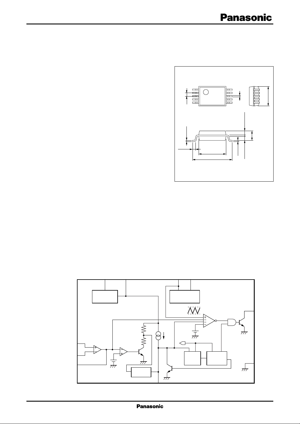
• Using 10-pin small outline package of 0.5 mm pitch
0.5±0.2
1
5
0.5
0.1±0.1
4.3±0.30
6.3±0.30
SSOP010-P-0225
10
6
+0.1
–0.05
0.15
Unit: mm
0.2±0.1
0.625±0.100.625±0.10
3.0±0.30
1.5±0.2
■ Applications
• LCD displays, digital still cameras, and PDAs
■ Block Diagram
IN+
IN−
FB
Error amp.
8
9
10
CC
V
6
Reference
supply
2.46 V
(allowance : ± 3%)
S.C.P. comp.
1.83 V
REF
V
7
CT1RT
2
0.5 V
Triangular
wave OSC
I
1.2 V
0.37 V
V
REF
SR
Latch
PWM
comparator
1.11 V
RO
U.V.L.O.
5
4
Out
GND
Clamp
3
S.C.P.
1
Page 2
AN8015SH Voltage Regulators
■ Pin Descriptions
Pin No. Symbol Description
1 CT Pin for connecting oscillator timing capacitor
2 RT Pin for connecting oscillator timing resistor
3 S.C.P. Pin for connecting the time constant setting capacitor for short-circuit protection
4 GND Grounding pin
5 Out Open collector type output pin
6VCCPower supply voltage application pin
7V
REF
8IN+ Error amplifier noninverted input pin
9IN− Error amplifier inverted input pin
10 FB Output pin of error amplifier
■ Absolute Maximum Ratings
Parameter Symbol Rating Unit
Supply voltage V
IN− terminal allowable application voltage V
IN+ terminal allowable application voltage V
Output terminal allowable application voltage V
Collector output current I
Power dissipation
Operating ambient temperature
Storage temperature
Note)*: Expect for the power dissipation, operating ambient temperature, and storage temperature, all ratings are for Ta = 25°C.
Reference voltage output pin
*
*
*
OUT
P
T
T
CC
IN−
IN+
OUT
D
opr
stg
35 V
− 0.3 to V
− 0.3 to V
REF
REF
35
100 mA
154 mW
−30 to +85 °C
−55 to +150 °C
■ Recommended Operating Range
Parameter Symbol Range Unit
Error amplifier input voltage V
Collector output voltage V
Collector output current I
Timing capacitance C
Timing resistance R
Oscillation frequency f
Reference voltage output current I
Soft start short-circuit protection time C
constant setting capacitance
2
OUT
OUT
OUT
RE
SCP
IN
− 0.1 to 0.8 V
34 (maximum) V
50 (maximum) mA
T
T
100 to 27 000 pF
5.6 to 15 kΩ
2 to 500 kHz
−3 to 0 mA
1 000 (minimum) pF
Page 3
Voltage Regulators AN8015SH
■ Electrical Characteristics at VCC = 12 V, RT = 15 Ω, CT = 200 pF, Ta = 25°C
Parameter Symbol Conditions Min Typ Max Unit
Reference voltage block
Reference voltage V
Input regulation with input fluctuation
Input regulation with input fluctuation 2
REFIREF
Line
Line2 VCC = 3.6 V to 20 V 10 mV
Load regulation Load I
Output voltage temperature V
TC1
characteristics 1
Output voltage temperature V
TC2
characteristics 2
Reference short-circuit current I
RS
U.V.L.O. block
Circuit operation start voltage V
Hysteresis width V
UON
HYS
Error amplifier block
Input offset voltage V
Input bias current I
Common-mode input voltage range V
High-level output voltage V
Low-level output voltage V
Output sink current I
Output source current I
Open-loop gain A
IO
B
ICR
EH
EL
SINK
SOURCEVFB
V
Common-mode ripple rejection ratio CMRR 50 dB
Output block
Oscillation frequency f
Maximum duty ratio Du
Output saturation voltage V
Output leak current I
RT terminal voltage V
Maximum oscillation frequency f
Frequency supply voltage f
OUT
maxRT
OLIO
LEAKVCC
RT
OUT(max)RT
dV
characteristics VCC = 3.6 V to 34 V
Frequency temperature characteristics 1
Frequency temperature characteristics 2
f
dT1fOUT
f
dT2fOUT
= −1 mA 2.386 2.46 2.534 V
VCC = 3.6 V to 34 V, I
= − 0.1 mA to −1 mA 210mV
REF
= −1 mA
REF
520mV
Ta = −30°C to +25°C ± 0.5 %
Ta = 25°C to 85°C ± 0.5 %
−20 mA
2.8 3.1 3.4 V
100 200 300 mV
−6 6mV
−500 −25 nA
− 0.1 0.8 V
V
− 0.3 V
− 0.1
REF
REF
V
0.1 0.3 V
VFB = 0.8 V 8 mA
= 0.8 V −120 µA
70 dB
RT = 15 kΩ, CT = 200 pF 175 195 215 kHz
= 15 kΩ, CT = 200 pF 85 90 95 %
= 50 mA, RT = 15 kΩ0.9 1.2 V
= 34 V, 10 µA
when output transistor is off
0.5 V
= 5.6 kΩ, CT = 150 pF 500 kHz
f
= 200 kHz, ±2 %
OUT
= 200 kHz,
±3 %
Ta = −30°C to +25°C
= 200 kHz,
±3 %
Ta = 25°C to 85°C
3
Page 4
AN8015SH Voltage Regulators
■ Electrical Characteristics at VCC = 12 V, RT = 15 Ω, CT = 200 pF, Ta = 25°C (continued)
Parameter Symbol Conditions Min Typ Max Unit
Short-circuit protection circuit block
Input threshold voltage V
Input standby voltage V
Input latch voltage V
Charge current I
Comparator threshold voltage V
THPC
STBY
IN
CHG
THL
V
= 0 V −1.32 −1.1 − 0.88 µA
SCP
Whole device
Total consumption current I
Total consumption current 2 I
RT = 15 kΩ1.8 2.8 mA
CC
RT = 5.6 kΩ, CT = 150 pF 2.5 mA
CC2
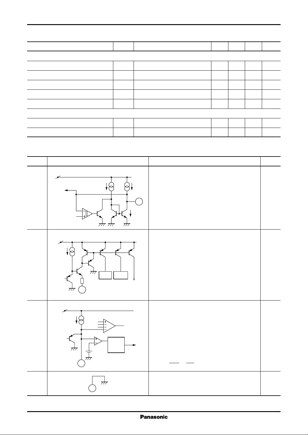
■ Terminal Equivalent Circuits
Pin No. Equivalent circuit Description I/O
1 CT: O
V
REF
To PWM input
OSC
comp.
210
The terminal used for connecting a timing capacitor to set oscillation frequency.
I
O
Use a capacitance value within the range of 100 pF
to 27 000 pF.
1
Use a oscillation frequency in the range of 2 kHz
to 500 kHz.
1.73 1.83 1.93 V
1.15 1.25 1.35 V
30 120 mV
1.83 V
2 RT: I
V
REF
The terminal used for connecting a timing resistor
to set oscillation frequency.
Use a resistance value within the range of 5.6 kΩ
to 15 kΩ . The terminal voltage is 0.5 V typ.
OSC PWM
100 Ω
2
RT(VRT ≈ 0.5 V)
3 S.C.P.: O
V
REF
S.C.P.
The terminal used for connecting a capacitor to set
I
CHG
CT
PWM
the time constant of soft start and timer latch shortcircuit protection circuit.
S.C.P.
Latch
S
Q
R
1.83 V
3
Use a capacitance value in the range of more than
1 000 pF.
The charge current is about 1.1 mA at R
V
I
CHG
RT
=
R
T
×1[A]
30
= 15 kΩ
T
4 GND:
Grounding terminal
4
4
Page 5
Voltage Regulators AN8015SH
■ Terminal Equivalent Circuits (continued)
Pin No. Equivalent circuit Description I/O
5 Out: O
V
REF
Open-collector type (darlington) output terminal.
The absolute maximum rating of output current is
5
100 mA
Use with a steady-state output current under 50
mA.
6V
6
:
CC
The terminal for applying supply voltage.
Use with a operating supply voltage within the
range of 3.6 V to 34 V.
7V
V
CC
V
overcurrent detection
REF
:O
REF
The output terminal for the reference voltage (2.46
V)
Use with a load current −3 mA or under.
This terminal is incorporating the short-circuit
Bias to other block
7
protection circuit, and the short-circuit current is
about −20 mA. Use the V
for the reference
REF
input setting of the error amplifier.
8IN+:I
V
REF
The noninverted input terminal of the error amplifier.
For common-mode input, use in the range of − 0.1
V to +0.8 V.
9IN−:I
89
The inverted input terminal of the error amplifier.
For common-mode input, use in the range of − 0.1
V to +0.8 V.
10 FB: O
V
REF
120 µA
CT
PWM
The output terminal of the error amplifier.
The source current is about −120 µA, and the sink
current is about 8 mA.
Correct the frequency characteristics of the gain
8 mA
10
and the phase by connecting a resistor and a capacitor between this terminal and IN− terminal.
5
Page 6

AN8015SH Voltage Regulators
■ Application Notes
[1] Main characteristics
Reference voltage temperature characteristics Maximum duty ratio temperature characteristics
(V)
REF
2.50
2.49
2.48
2.47
VCC = 12 V
I
= −1 mA
REF
(%)
max
91.0
90.5
90.0
VCC = 12 V
C
= 200 pF
T
= 15 kΩ
R
T
Reference voltage V
2.46
2.45
−40 −20 100
Ambient temperature Ta (°C)
806040200
89.5
Maximum duty ratio Du
89.0
−40 −20 100
Ambient temperature Ta (°C)
806040200
Oscillation frequency temperature characteristics Timing capacitance Oscillation frequency
200
195
(kHz)
OUT
190
185
VCC = 12 V
C
= 200 pF
T
R
= 15 kΩ
T
Oscillation frequency f
180
−40 −20 100
806040200
Ambient temperature Ta (°C)
Maximum duty ratio Oscillation frequency
(%)
max
Maximum duty ratio Du
100
90
R
T
80
R
T
= 15 kΩ
= 5.6 kΩ
VCC = 12 V
= 25°C
T
a
1 M
RT = 5.6 kΩ
VCC = 12 V
T
= 25°C
a
(Hz)
100 k
OUT
10 k
= 15 kΩ
R
T
RT = 10 kΩ
Oscillation frequency f
1 k
100 00010 0001 000100
Timing capacitance CT (pF)
Oscillation frequency Triangular wave maximum
amplitude voltage
1.4
(V)
1.2
1.0
0.8
0.6
0.4
0.2
VCC = 12 V
R
= 15 kΩ
T
T
= 25°C
a
70
10k 100k 1M
Oscillation frequency f
6
OUT
(Hz)
Triangular wave maximum amplitude voltage
0
10k 100k 1M
Oscillation frequency f
OUT
(Hz)
Page 7

Voltage Regulators AN8015SH
■ Application Notes (continued)
[1] Main characteristics (continued)
Supply voltage Reference voltage Supply voltage Total consumption current
(V)
REF
3.0
Ta = 25°C
= −1 mA
I
REF
2.5
2.0
1.5
(mA)
CC
3.0
Ta = 25°C
2.5
RT = 5.6 kΩ
2.0
RT = 15 kΩ
1.5
1.0
1.0
Reference voltage V
0.5
0
05
1
2 3 4
0.5
Total consumption current I
0
05
Supply voltage VCC (V)
Reference voltage line regulation Total consumption current line regulation
2.52
2.50
Ta = 25°C
I
REF
(V)
REF
2.48
2.46
Reference voltage V
2.44
2.42
05 35
Supply voltage VCC (V)
= −1 mA
3025201510
3.0
(mA)
CC
2.5
2.0
Total consumption current I
1.5
05 35
1
2 3 4
Supply voltage VCC (V)
RT = 5.6 kΩ
RT = 15 kΩ
Supply voltage VCC (V)
Ta = 25°C
3025201510
Timing resistance Total consumption current Timing resistance Output saturation voltage
0.85
0.84
(V)
OL
0.83
0.82
0.81
Output saturation voltage V
0.80
420
8 12 16
VCC = 12 V
T
= 25°C
a
I
= 50 mA
O
Timing resistance RT (kΩ)
(mA)
CC
2.5
2.0
1.5
VCC = 12 V
= 25°C
T
a
Total consumption current I
1.0
420
8 12 16
Timing resistance RT (kΩ)
7
Page 8

AN8015SH Voltage Regulators
■ Application Note (continued)
[2] Timing chart
3.1 V typ.
V
REF
(V
t
r
rise time
) ≥ 10 [µs]
REF
Lock-out release
Supply voltage (V
Reference voltage (V
CC
REF
)
3.6 V
)
2.46 V
Error amplifier output (FB)
Power supply
on
Triangular wave (CT)
S.C.P. terminal voltage
Output transistor collector waveform
(Out)
Figure 1. PWM comparator operation waveform
Reference voltage (V
REF
)
Short-circuit protection input threshold level
Comparator threshold level
S.C.P. terminal voltage
Dead-time voltage (V
DT
)
Error amplifier output (FB)
Triangular
wave (CT)
Output transistor
collector waveform (Out)
Dead-time voltage (V
DT
)
Soft start operation Maximum duty 90%
1.83 V
1.20 V
1.11 V
0.37 V
High
Low
2.46 V
1.83 V
1.20 V
1.11 V
0.37 V
0.03 V
High
Low
Short-circuit protection
comparator output
8
Figure 2. Short-circuit protection operation waveform
t
PE
High
Low
Page 9

Voltage Regulators AN8015SH
■ Application Notes (continued)
[3] Function descriptions
1. Reference voltage block
This block is composed of the band gap circuit, and outputs the temperature compensated 2.46 V reference
voltage to the V
and used as the operating power supply for the IC inside. It is possible to take out a load current of up to −3 mA .
Also, an overcurrent protection circuit is built in for the load, thereby protecting the IC from destruction when
V
terminal is short circuited.
REF
2. Triangular wave oscillation block
The triangular wave which swings from the highest wave of approximately 1.4 V to the lowest wave of
approximately 0.37 V will be generated by connecting a timing capacitor and a resistor to the CT terminal (pin 1) and
RT terminal (pin 2) respectively. The oscillation frequency can be freely decided by the value of C
connected externally.
The triangular wave is connected with the inverted input of PWM comparator of the IC inside.
3. Error amplifier block
This block detects the output voltage of DC-DC converter by the PNP transistor input type error amplifier, and
inputs the amplified signal to the PWM comparator.
The common-mode input voltage range is − 0.1 V to 0.8 V, and is a voltage obtained by dividing the reference
voltage with resistors.
Also, it is possible to perform the gain setting and the phase compensation arbitrarily by inserting the feedback
resistor and capacitor between the error amplifier output terminal (pin 10) and the inverted input terminal (pin 9).
The output voltage V
noninverted input terminal as shown in figure 3. 1), and the output voltage V
connecting to the inverted input terminal as shown in figure 3. 2). The output voltages in each of these cases are
given in the following equations.
terminal (pin 7). The reference voltage is stabilized when the supply voltage is 3.6 V or higher,
REF
T
, if positive, is obtained by connecting the resistor-divided reference voltage to the
OUT
, if negative, is obtained by
OUT
and R
T
R1
R2
V
OUT
V
= V
V
R3
R4
OUT
IN+
= V
IN+
REF
V
REF
IN+ 8
IN− 9
1) If output is positive
R1 + R2
×
×
R3 + R4
7
R
C
R2
R4
Error amp.
NF
NF
PWM comparator
input
FB 10
R1
R2
V
V
= − (V
OUT
IN−
R3
R4
V
= V
OUT
REF
REF
V
REF
IN+ 8
IN− 9
2) If output is negative
− V
×
R1 + R2
R2
7
R
C
R3 + R4
×
)V
IN−
Error amp.
NF
NF
R3
REF
PWM comparator
input
FB 10
Figure 3. Connection method of error amplifier
4. Timer latch short-circuit protection circuit
This circuit protects the external main switching devices, flywheel diodes, and choke coils, etc. from
destruction or deterioration if overload or short-circuit of power supply output lasts for a certain time.
The timer latch short-circuit protection circuit detects the output level of the error amplifier. When the output
voltage of DC-DC converter drops and the output level of error amplifiers exceeds 1.85 V, the low-level output is
given and the timer circuit is actuated to start the charge of the external protection enable capacitor.
If the output of the error amplifier does not return to a normal voltage range by the time when the voltage of
this capacitor reaches 1.83 V, it sets the latch circuit, cuts off the output drive transistor, and sets the dead-time at
100%.
9
Page 10

AN8015SH Voltage Regulators
■ Application Notes (continued)
[3] Function descriptions (continued)
5. Low input voltage malfunction prevention circuit (U.V.L.O.)
This circuit protects the system from destruction or deterioration due to control malfunction when the supply
voltage is low in the transient state of power on/off.
The low input voltage malfunction prevention circuit detects the internal reference voltage which changes
according to the supply voltage level. Until the supply voltage reaches 3.1 V during its rise time, it cuts off the the
output drive transistor, sets the dead-time at 100% and holds the S.C.P. terminal (pin 3) to low level. During the
fall time of the power supply voltage, it has hysteresis width of 200 mV and operates 2.9 V or less.
6. PWM comparator block
The PWM comparator controls the on-period of the output pulse according to the input voltage. It turns on the
output transistor during the period when the triangular wave of CT terminal (pin 1) of noninverted input is lower
than any one of the following voltages : the voltage of the error amplifier output (pin 10) of the inverted input, S.C.P.
terminal (pin 3), and the voltage for dead-time which is fixed inside the IC.
The S.C.P. terminal voltage is kept at 1.25 V in the state in which DC-DC converter output is stabilized.
However, when the power supply is turned on, the soft start is activated, which gradually extends on-period
according to the time constant determined by the capacitance of externally attached capacitor and the charge current.
The maximum duty ratio is fixed at approximately 90% by the voltage for dead-time.
7. Output block
The output drive transistor is of open-collector type output connected in darlington circuit of emitter common
GND. The breakdown voltage of collector output terminal (pin 5) is 34 V and it is possible to obtain up to 100 mA
output current.
[4] Triangular wave oscillation circuit
1. Oscillation frequency setting method
The waveform of triangular wave oscillation is obtained by charging and discharging of the constant current
I
from the external timing capacitor CT which is connected to CT terminal (pin 1). The constant current is set by
O
the externally attached timing resistor R
The peak value of the wave V
value of the wave V
are fixed at approximately 1.4 V
CTL
.
T
and the trough
CTH
V
CTH
typical and 0.37 V typical respectively.
The oscillation frequency f
following formula;
f
OSC
1
=
t1 + t
2
whereas IO = 2 ×
because V
f
=
OSC
CTH
1
1.66 × C
The output frequency f
=
2 × CT × (V
V
R
− V
× R
T
T
is obtained by the
OSC
I
RT
= 2 ×
T
= 0.83 V
CTL
is equal to f
OUT
O
CTH
0.5
R
− V
)
CHL
T
since it is PWM-controlled.
OSC
V
t
t
Charging Discharging
2
1
CTL
T
Figure 4. Triangular wave oscillation waveform
= 1.4 V typ.
= 0.37 V typ.
10
Page 11

Voltage Regulators AN8015SH
■ Application Notes (continued)
[4] Triangular wave oscillation circuit (continued)
2. Usage notes
This IC uses the constant current given by the timing resistor R
block and the PWM comparator for consumption current reduction. The total consumption current is approximately
1.8 mA (typical) when R
is 15 kΩ, and it increases to approximately 2.5 mA (typical) when RT is 5.6 k Ω. In order
T
to obtain the steady-state output current of 100 mA at the open collector output, it is necessary to set R
15 kΩ or smaller.
It is possible to use the circuit in the recom-
mended operating range of 2 kHz to 500 kHz of the
oscillation frequency. However, the timing resistor
R
versus the oscillation frequency should be set
T
within the recommended range shown in figure 5.
Also, refer to the "Applications Notes, [1] Main
characteristics, Timing capacitance Oscillation
frequency" for setting the timing capacitance.
For a high frequency use, the overshoot and un-
dershoot amounts increase due to operation delay
of the triangular oscillation comparator, and the
maximum duty ratio drops. This effect can be alleviated by speeding up through the reduction of the
resistor R
and increase in the circuit current.
T
Note that this IC can not be used as an IC for
slave when the several ICs are operated in parallel
synchronous mode.
as the bias current of the triangular oscillation
T
value to
T
1 M
500 k
(Hz)
Oscillation frequency f
100 k
OUT
10 k
1 k
Recommended operating
condition
10 k
Timing resistance RT (Ω)
15 k5 k 5.6 k
Figure 5. Timing resistance recommended condition
[5] Time constant setting method for short-circuit protection circuit with joint-use of soft start/timer latch type
The constructional block diagram of protection latch circuit is shown in figure 6. The comparator for short-circuit
protection compares the output of error amplifier V
with the reference voltage of 1.85 V at all the time.
FB
When the load conditions of DC-DC converter output is stabilized, there is no fluctuation of error amplifier
output and the short-circuit protection comparator also keeps the balance. At this moment, the output transistor Q1 is
in the conductive state and the S.C.P. terminal is hold to approximately 1.25 V through the clamp circuit.
When the load conditions suddenly change, and high-level signal (1.85 V or higher) is input from the error amplifier
to the noninverted input of the short-circuit protection comparator, the short-circuit protection comparator outputs the
low-level signal. Since this signal cuts off the output transistor Q1, the S.C.P. terminal voltage V
externally connected capacitor C
= V
V
PE
1.83 V = 1.25 V + I
CS = I
I
is the constant current determined by the oscillation timing resistor RT and its dispersion and fluctuation with
CHG
temperature are small. I
I
CHG
V
is approximately 0.5 V and I
RT
+ I
t
PE
0.58
×
1
30
CHG
×
CHG
[F]
CHO
[A]
STBY
×
CHG
V
RT
=
R
T
starts charging according to the following equation:
S
t
PE
[V]
C
S
t
PE
×
C
S
is expressed in the following equation:
becomes approximately 1.1 µA when RT = 15 kΩ.
CHO
is released, and the
PE
11
Page 12

AN8015SH Voltage Regulators
■ Application Notes (continued)
[5] Time constant setting method for short-circuit protection circuit with joint-use of soft start/timer latch type
(continued)
When the external capacitor C
output drive transistor by enabling the low input voltage malfunction prevention circuit, and sets the dead-time at 100%.
The low input voltage malfunction prevention circuit is once enabled, the S.C.P. terminal voltage is discharged to
approximately 30 mV but the latch circuit is not reset unless the power is turned off.
The S.C.P. terminal voltage is inputted to the PWM comparator, and the soft start is actuated when the power turns
on. However, since at the beginning of power on, the error amplifier output is high level, and V
voltage is released and charging begins; the external capacitor should be set so that the output voltage of DC-DC
convertor starts to rise before the latching circuit is set. The charging equation is as same as the above. The soft start
time t
until the input standby voltage V
SS
1.25 V = 0.03 V + I
tSS = 1.22 ×
Error amp.
8
IN+
9
IN−
10
FB
I
C
CHG
CHG
S
[s]
has been charged up to approximately 1.83 V, it sets the latch circuit, cuts off the
S
of S.C.P. terminal
PE
becomes 1.25 V is given in the following equations:
STBY
t
SS
×
C
S
I
1.25 V
S.C.P. comp.
Q1
CHG
Clamp
circuit
SR
Latch
Q2
PWM comparator input
R
U.V.L.O.
Output cut-off
1.83 V
3
V
REF
C
S
S.C.P.
Figure 6. Short-circuit protection circuit
12
Page 13

Voltage Regulators AN8015SH
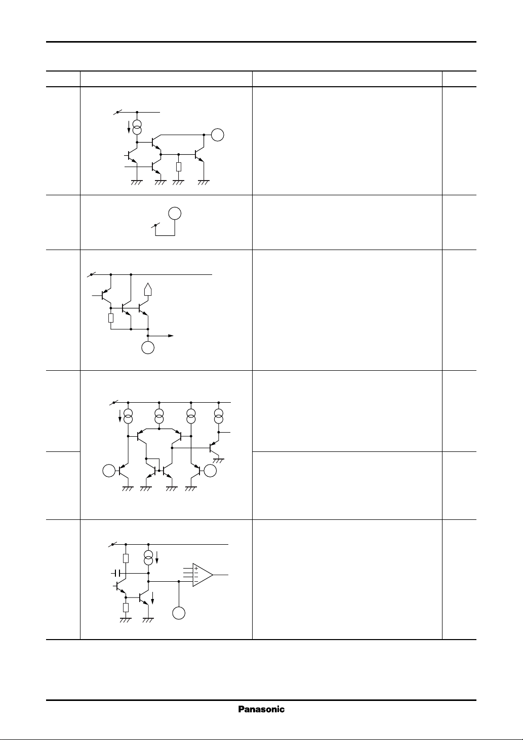
■ Application Circuit Examples
1. Chopper method step-down type
V
120 kΩ
CC
1 000 pF
3.6 kΩ
FB10
1
CT
IN−9
2
RT
200 pF 0.1 µF15 kΩ
2. Chopper method inverting type
120 kΩ
3.6 kΩ
1 000 pF
FB10
IN−9
0.1 µF
8.2 kΩ
IN+8
3
S.C.P.
REF7
V
4
GND
130 kΩ
CC6
V
5
Out
V
CC
0.1 µF
8.2
9.1
kΩ
kΩ
IN+8
REF
V
7
CC
V
6
25.5 kΩ
SBD
4.5 kΩ
SBD
V
5 V
V
O
−24 V
O
1
CT
2
RT
200 pF 0.1 µF15 kΩ
3
S.C.P.
4
GND
5
Out
13
Page 14

AN8015SH Voltage Regulators
■ Application Circuit Examples (contined)
3. On/off circuit example
C7
V
CC
V
Q1
I
CC
SBD
1) Method to cut V
Standby current ≈ 0 µA
CC
line
O
FB
10
1
CT
IN−
9
2
RT
2) Method to cut S.C.P. line
Consumption current
when output off ≈ 1.8 mA
FB
10
IN−
9
REF
IN+
V
8
3
7
4
GND
S.C.P.
CC
V
C8
On/off
6
5
Out
V
CC
V
O
C8
I
REF
V
7
CC
CC
V
6
C7
IN+
8
SBD
1
CT
2
3
RT
S.C.P.
4
GND
5
Out
Q2
On/off
4. Using method
Since the on/off circuit is not incorporated in this IC, it is required to add on/off circuit externally to provide a
standby function.
When the switch (Q1) is inserted between the V
line and the Vcc pin of the IC (pin 6) as shown in 3. 1), the standby
CC
current is suppressed to 0. When the output is turned off by decreasing the S.C.P. terminal voltage below the lower
limit of the triangular wave (0.37 V typical) as shown in 3. 2), the consumption current does not decrease because the
IC is operating.
5. Usage notes
The rise time of the V
latch circuit of the IC is set so that the circuit fails to start. Adjust C7 or C8 so that the rise time for V
becomes sharp especially in the case of 3. 1). At that time, there is a case that the internal
CC
pin (pin 7)
REF
becomes 10 ms or longer.
14
 Loading...