

Page 1
Voltage regulators
0.3
(0° to 10°)
(0.15)
10.1±0.3
4.2±0.3
6.5±0.3
18
16 9
1.27
(0.605)
Seating plane Seating plane
0.40±0.25
0.1±0.1 1.5±0.2
AN8014S
Step-down, step-up, or inverting DC-DC converter control IC
■ Overview
The AN8014S is a single-channel PWM DC-DC
converter control IC.
This IC can provide any one output type from
among step-down, step-up and inverting output.
Allowing n-channel power MOSFET direct driving, the AN8014S is ideal for high-efficiency power
supplies.
■ Features
• Wide operating supply voltage range (3.6 V to 34 V)
(The voltage is limited within a range between 3.6
V and 17 V if it is connected to a step-down voltage circuit.)
•
Totem pole output circuit: output peak current (±1 A)
• On-chip pulse-by-pulse overcurrent detection and
protection circuit
Threshold voltage V
− 0.095 V typical
CC
• On-chip bootstrap circuit (allowing n-channel MOSFET direct driving.)
• On-chip under-voltage lock-out circuit (U.V.L.O.)
• On-chip on/off function (active-high control input, standby current of maximum 5 µA)
• On-chip timer latch short-circuit protection circuit
• Maximum oscillator frequency (500 kHz)
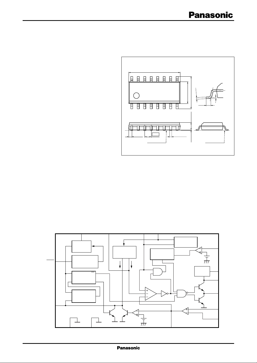
SOP016-P-0225A
Unit: mm
■ Applications
• DC-DC switching power supply
■ Block Diagram
16
OFF
5
S.C.P.
11
V
2.5V
On/off
active-high
R
U.V.L.O.
S
R
Latch
S
SGND
1
REF
V
REF
12
Q
Q
Q
PGND
DTC
4
Constant
current
source
1 µA 10 µA
S.C.P.
comp.
CT
3
2
Latch
RQS
PWM
comp.
RT
8
FB
Triangular
wave OSC
Error amp.
Boot
strap
10
CLM
15
V
CC
14
CB
13
Out
6
IN+
7
IN−
1
Page 2

AN8014S Voltage regulators
■ Pin Descriptions
Pin No. Description
1 Internal reference output
2 Oscillator timing resistor connection
3 Oscillator timing capacitor connection
4 Dead-time control
5 Capacitance connection for short-circuit
protection delay
6 Error amplifier noninverting input
7 Error amplifier inverting input
8 Error amplifier output
■ Absolute Maximum Ratings
Parameter Symbol Rating Unit
Supply voltage V
Supply current I
2
Power dissipation
Operating ambient temperature
Storage temperature
*
1
*
1
*
On/off pin allowable application voltage V
Error amplifier allowable input voltage V
DTC pin allowable application voltage V
Out pin allowable application voltage V
Out pin constant output current I
Out pin peak output current I
CB pin allowable application voltage V
CB pin constant output current I
CB pin peak output current I
CLM pin allowable application voltage V
Note) 1.*1: Except for the operating ambient temperature and storage temperature, all ratings are for Ta = 25°C.
2: At Ta = 85°C
*
2. Do not apply external currents or voltages to any pins not specifically mentioned.
For circuit currents, '+' denotes current flowing into the IC, and '−' denotes current flowing out of the IC.
CC
CC
P
D
T
opr
T
stg
ON/OFF
I
DTC
OUT
O
O(Peak)
CB
CB
CBP
CLM
Pin No. Description
9 Not connected
10 Overcurrent protection input
11 Signal ground
12 Output stage ground
13 Totem pole type output
14 Bootstrap output
15 Supply voltage
16 On/off control
35 V
mA
143 mW
−30 to +85 °C
−40 to +125 °C
V
CC
− 0.3 to V
− 0.3 to V
REF
REF
35 V
±100 mA
±1 000 mA
35 V
−100, 150 mA
−500, 1 000 mA
V
CC
V
V
V
V
■ Recommended Operating Range
Parameter Symbol Range Unit
Supply voltage V
2
CC
Step-up circuit system 3.6 to 34 V
Step-down circuit system 3.6 to 17
Page 3

Voltage regulators AN8014S
■ Electrical Characteristics at V
= 12 V, Ta = 25°C
CC
Parameter Symbol Conditions Min Typ Max Unit
Reference voltage block
Output voltage V
Line regulation with input fluctuation
REFIREF
Line VCC = 3.6 V to 34 V 16 25 mV
Load regulation Load I
U.V.L.O. block
Circuit operation start voltage V
Hysteresis width V
UON
HYS
Error amplifier block
Input offset voltage V
Input bias current I
Common-mode input voltage range V
High-level output voltage V
Low-level output voltage V
IO
B
ICR
EH
EL
Dead-time control circuit block
Input current I
Low-level input threshold voltage V
High-level input threshold voltage V
DTC
DT-L
DT-H
Output block
Oscillator frequency f
OUT
Output duty Du R
Low-level output voltage V
High-level output voltage V
OLIO
OHIO
Bootstrap circuit block
Input standby voltage V
INCBICB
Short-circuit protection circuit block
Input threshold voltage V
Input standby voltage V
Input latch voltage V
Charge current I
THPC
STBY
IN
CHG
On/off control block
Threshold voltage V
TH
Overcurrent protection block
Threshold voltage V
CLM
= −1 mA 2.522 2.6 2.678 V
= − 0.1 mA to −1 mA 110mV
REF
2.8 3.1 3.4 V
60 140 180 mV
−6 6mV
−500 −25 nA
− 0.1 0.8 V
V
REFVREF
V
− 0.3 − 0.1
0.1 0.3 V
−15.8 −13.2 −10.6 µA
Duty 0% 0.45 0.65 V
Duty 100% 1.2 1.4 V
CT = 120 pF, RT = 15 kΩ 196 218 240 kHz
= 75 kΩ 47 52 57 %
DTC
= 70 mA 1.0 1.3 V
= −70 mA V
CB
V
CB
V
−2.0 −1.0
= −70 mA V
CC
V
CCVCC
V
−1.2 −1.0 − 0.8
0.70 0.75 0.80 V
30 120 mV
30 120 mV
−2.76 −2.30 −1.84 µA
0.8 2.0 V
V
CC
V
CCVCC
V
− 0.115− 0.095− 0.075
3
Page 4

AN8014S Voltage regulators
■ Electrical Characteristics at V
= 12 V, Ta = 25°C (continued)
CC
Parameter Symbol Conditions Min Typ Max Unit
Whole device
Total consumption current I
Standby current I
CC
CC(SB)
5.0 7.0 mA
5 µA
• Design reference data
Note) The characteristics listed below are theoretical values based on the IC design and are not guaranteed.
Parameter Symbol Conditions Limit Unit
Reference voltage block
Output voltage temperature V
Ta = −30°C to +25°C ±1%
TC1
characteristics 1
Output voltage temperature V
Ta = 25°C to 85°C ±1%
TC2
characteristics 2
Output short-circuit current I
OS
−40 mA
Error amplifier block
Output sink current I
Output source current I
SOURCEVFB
Open-loop gain A
SINKVFB
G
= 0.9 V 8 mA
= 0.9 V −110 µA
70 dB
Output block
f
Frequency supply voltage f
dV
= 200 kHz, ±3%
OUT
characteristics VCC = 3.6 V to 34 V
Frequency temperature f
dT1
f
= 200 kHz, ±9%
OUT
characteristics 1 Ta = −30°C to +25°C
f
Frequency temperature f
dT2
= 200 kHz, ±9%
OUT
characteristics 2 Ta = 25°C to 85°C
Oscillator block
RT pin voltage V
RT
0.4 V
Short-circuit protection circuit block
Comparator threshold voltage V
THL
1.87 V
Overcurrent protection circuit block
Delay time t
DLY
200 ns
4
Page 5
Voltage regulators AN8014S
■ Terminal Equivalent Circuits
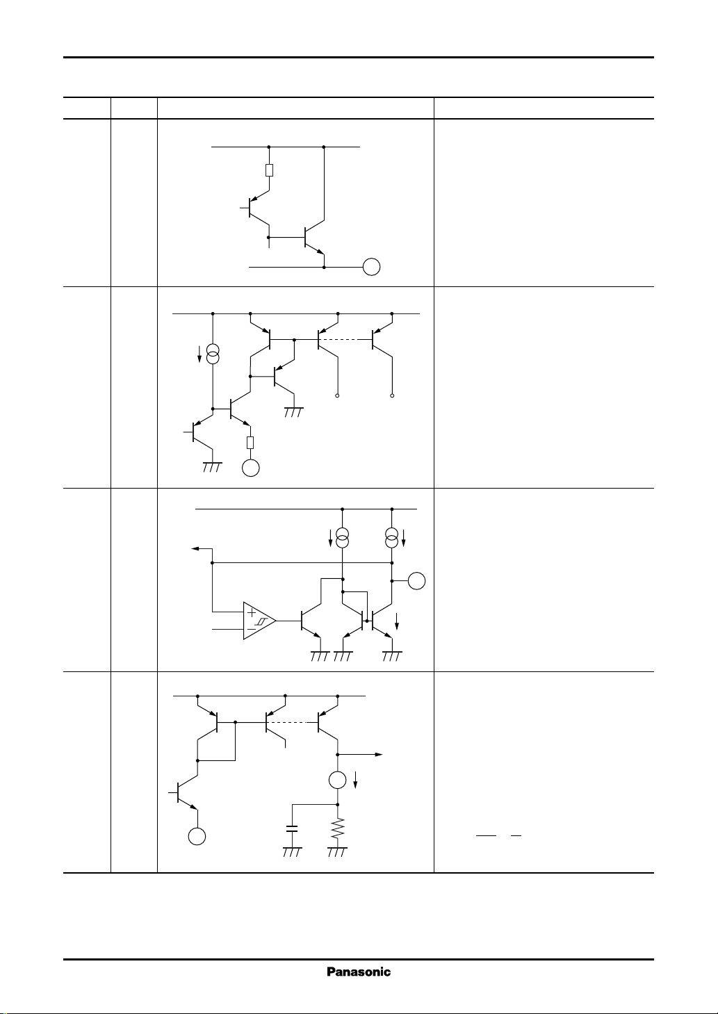
Pin No. I / O Equivalent circuit Description
1O V
V
CC
REF
:
Outputs the reference voltage
Incorporating short-circuit protection
against ground.
V
REF
1
2 RT:
V
REF
Connection for the timing resistor which
decides the oscillator frequency. Use a resistor in the range 5.1 kΩ to 30 kΩ. The
pin voltage is approx. 0.4 V.
DTC S.C.P.
100 Ω
RT(≈ 0.4 V)
2
3 CT:
V
REF
To PWM input
Connection for the timing capacitor which
decides the oscillator frequency. Use a ca-
I
O
pacitor in the range 100 pF to 10 000 pF.
CT
OSC
comp.
For the oscillator frequency setting, refer
3
to the "Application Notes, [1] Function
descriptions" section. Use an oscillator fre-
2I
O
quency in the range 5 kHz to 500 kHz.
2.6 V (allowance: 3%)
4 DTC:
V
REF
PWM comparator
input
Connection for a resistor and a capacitor
that set the dead-time and soft start period
of PWM output.
Input current I
I
4
R
DTC
DTC
DTC
C
DTC
2
resistor R
variations and temperature variations.
It is approx. −13.2 µA when RT = 15 kΩ.
I
DTC
RT
is decided by the timing
DTC
which controls sample to sample
T
× 1
V
RT
=
RT2
[A]
5
Page 6
AN8014S Voltage regulators
■ Terminal Equivalent Circuits (continued)
Pin No. I / O Equivalent circuit Description
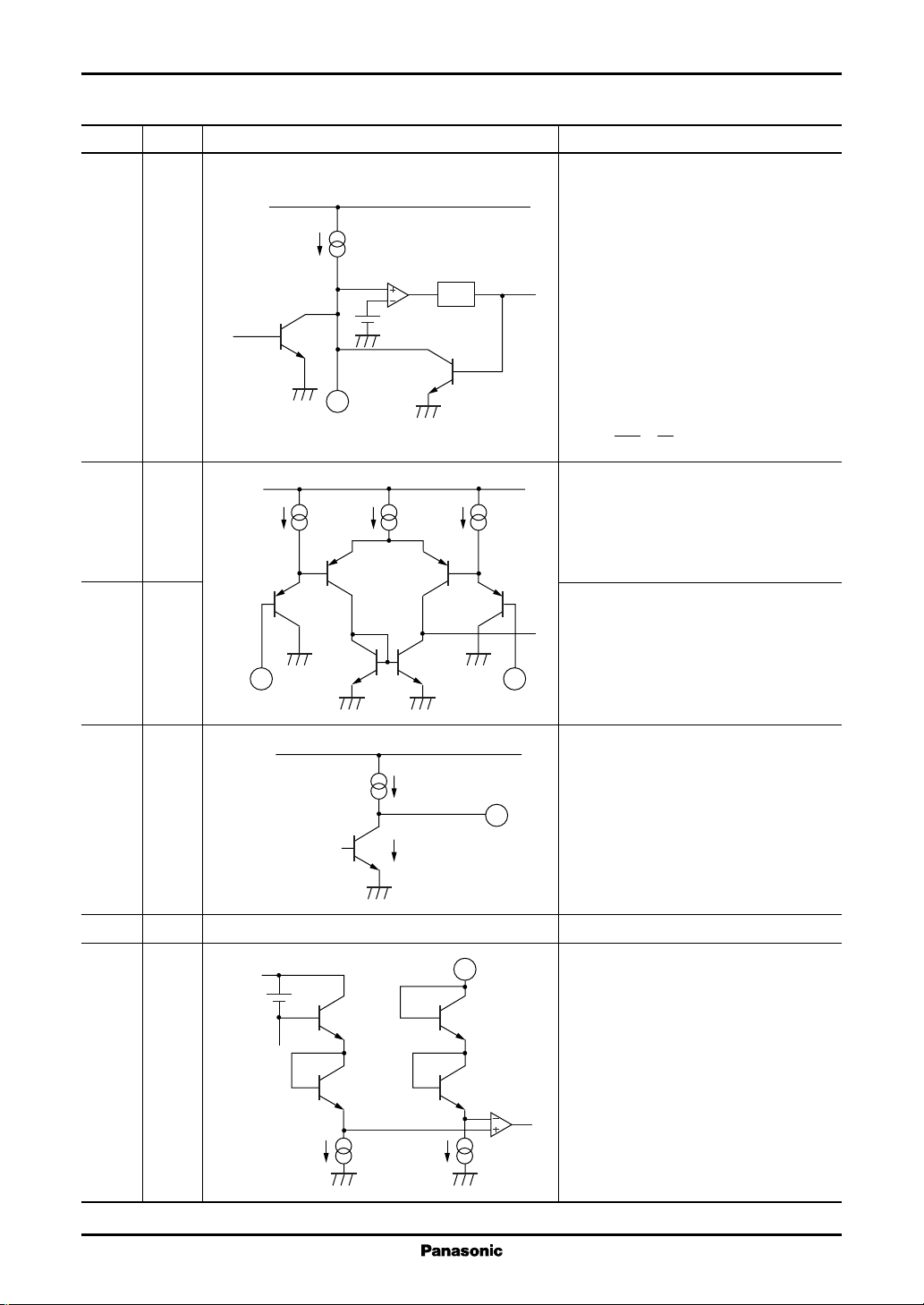
5 S.C.P.:
V
REF
I
CHG
Latch
S
Q
U.V.L.O.
output
6I IN+:
V
REF
5
0.75 V
S.C.P.
R
Connection for the capacitor that sets the
soft start period and the timer latch shortcircuit protection circuit time constant.
Use a capacitor with a value of 1 000 pF
or higher.
The charge current I
timing resistor R
is decided by the
CHG
which controls sample
T
to sample variations and temperature variations.
It is approx. −2.3 µA when R
VRT × 1
I
CHG
=
RT11
[A]
= 15 kΩ.
T
Noninverting input to the error amplifier.
Use the common-mode input in the range
− 0.1 V to +0.8 V.
7I IN−:
Inverting input to the error amplifier.
Use the common-mode input in the range
− 0.1 V to +0.8 V.
7 6
IN− IN+
8 O FB:
V
REF
Source current
8
FB
Output from the error amplifier.
The source current is approx. −110 µA and
sink current is approx. 8 mA.
Correct the frequency characteristics of
Sink current
the gain and the phase by connecting a resistor and a capacitor between this pin
and IN− pin.
9 N.C.: Not connected.
10 I CLM:
V
CC
0.1 V
10
CLM
Detects the overcurrent state in switching
transistor.
Insert a resistor with a low resistance between
this pin and VCC to detect overcurrent states.
CLM
comp.
When this pin falls to a level 95 mV or
more lower than V
turned off for that period thus narrowing
50 µA 50 µA
the width of the on-period.
(This implements a pulse-by-pulse
overcurrent protection technique.)
, the PWM output is
CC
6
Page 7

Voltage regulators AN8014S
■ Terminal Equivalent Circuits (continued)
Pin No. I / O Equivalent circuit Description
11 SGND: Signal ground.
SGND
11
12 GND: Output stage ground.
GND
12
13 O Out:
Totem pole output.
V
CC
14
CB
14 O CB:
Out
13
15 I V
15
V
CC
A constant output current of ±100 mA or a
peak output current of ±1 A can be ob-
tained.
Bootstrap output.
Connect a bootstrap capacitor between
this pin and the n-channel MOSFET sourceside pin of the switching element when
using a step-down voltage circuit.
Short-circuit this pin and the V
pin when
CC
using a step-up voltage circuit.
: Power supply.
CC
16 I
OFF
:
Controls the on/off state.
OFF
16
17 kΩ
13 kΩ
When the input is high: normal operation
(V
> 2.0 V)
OFF
When the input is low: standby mode
(V
< 0.8 V)
OFF
In standby mode, the total current consumption is held to under 10 µA.
■ Application Notes
[1] Function descriptions
1. Reference voltage block
This block is composed of the band gap circuit and outputs the temperature compensated reference voltage (2.6
V) to the V
as the operating power supply in IC. It is possible to take out a load current of up to −1 mA.
pin (pin 1). The reference voltage is stabilized when the supply voltage is 3.6 V or more and used
REF
7
Page 8

AN8014S Voltage regulators
■ Application Notes (continued)
[1] Function descriptions (continued)
2. The triangular wave generator block (OSC)
The triangular wave which swings from approximately 1.32 V (upper limit value, V
V (lower limit value, V
(pin 3) and R
pin (pin 2) respectively. Oscillator frequency can be freely decided by the value of CT and R
T
connected externally. The oscillator frequency f
=
≈
1
t1 + t
2
V
RT
R
T
CTH
2.59 × C
of approximately 215 kHz will be
OSC
f
OSC
I
= 1.7 ×
O
Because V
f
OSC
Example) An f
obtained if C
) will be generated by connecting a timing capacitor CT and a resistor RT to the CT pin
OSCL
is obtained by the following formula;
OSC
I
0.4
R
T
[Hz]
O
CTH
− V
CHL
)
t
1
Charging Discharging
t
2
T
Figure 1. Triangular oscillation waveform
=
2 × CT × (V
= 1.7 ×
− V
= 0.88 V
CTL
1
× R
T
T
is 120 pF and RT is 15 kΩ.
T
It is possible to use the circuit in the recommended operating range of 5 kHz to 500 kHz of the oscillator
frequency. As the AN8014S is used at increasingly higher frequencies, the amount of overshoot and undershoot
due to the operation delay in the triangular wave oscillator comparator increases, and discrepancies between the
values calculated as described previously and the actual values may occur.
The output source currents of the AN8014S's S.C.P. and DTC pins are determined by the timing resistor R
which is externally connected to the RT pin. Therefore, note that this IC can not be used as an IC for slave when
the several ICs are operated in parallel synchronous mode.
3. Error amplifier block
Detecting and amplifying DC-DC converter output voltage, the error amplifier with PNP transistor input inputs
the signal to the PWM comparator.
Figure 2 shows the way to connect the error amplifier.
The common-mode input voltage range is − 0.1 V to + 0.8 V, and a voltage obtained by dividing the reference
voltage with built-in resistors is applied to the non-inverting input. Connecting the feedback resistor and the
capacitor between the error amplifier output pin (pin 8) and the inverting input pin (pin 7) allows the arbitrary gain
setting and the phase compensation.
Startup overshooting caused by feedback delays will be suppressed by setting the output source current and
output sink current to as high as 110 µA and 8 mA respectively.
The input voltage V
V
= V
REF
×
IN+
IN+
R
4
R3 + R
and V
4
to the error amplifier are obtained from the following formulas.
IN−
R
V
= V
IN−
OUT
×
2
R1 + R
2
) to approximately 0.44
OSCH
V
= 1.32 V (typ.)
CTH
= 0.44 V (typ.)
V
CTL
T
T
1
V
REF
R3
IN+
IN−
6
7
PWM comparator
Error
amp.
CT
DTC
13
V
OUT
R1
R4
R
C
NF
8
NF
FB
R2
Figure 2. Connection method of error amplifier
8
Page 9

Voltage regulators AN8014S
■ Application Notes (continued)
[1] Function descriptions (continued)
4. Timer latch short-circuit protection circuit
This circuit protects external main switching devices, flywheel diodes, choke coils and so forth from breakdown
or deterioration when overload or short-circuit of power supply lasts a certain time.
Figure 3 shows the short-circuit protection circuit. The timer latch short-circuit protection circuit detects the
output level of the error amplifier.
If the output voltage of the DC-DC converter is stable, the output of the error amplifier from the FB pin is stable
and the short-circuit protection comparator is well balanced.
In that case, the transistor Q1 is conductive and the S.C.P. pin voltage is approximately 30 mV constantly.
If the load condition changes radically and output signal voltage of the error amplifier (FB) is 1.87 V or
higher, the short-circuit protection comparator outputs low-level voltage. Then, by cutting off the transistor Q1,
the external capacitor C
following formulas.
V
= V
PE
STBY
0.75 V = 0.03 V + I
CS = I
I
CHG
If R
I
CHG
×
CHG
is constant current which is determined by the timing resistor RT .
is 15 kΩ, I
T
V
RT
=
R
T
When the external capacitor C
the totem-pole output pin will be set to low level and the dead-time will be set to 100%.
When the latch circuit is turned on, the S.C.P. pin will discharge electricity till the voltage on the S.C.P. pin
reduces to approximately 30 mV. The latch circuit cannot be, however, reset until power supply to the AN8014S
is turned off.
of S.C.P. pin (pin 5) starts charging with the current I
S
t
+ I
t
0.72
×
PE
CHG
PE
CHG
×
CHG
[V]
C
S
t
PE
×
C
S
[F]
will be approximately 2.3 µA.
1
[A]
11
is charged up to approximately 0.75 V, the latch circuit will be turned on. Then
S
which is obtained from the
CHG
V
REF
Cut output off
IN+
IN−
FB
6
7
8
Error amp.
S.C.P.
comp.
1.82 V
I
CHG
Q1
S.C.P.
S
Q
Q
R
Latch
Q2
5
C
S
Figure 3. Short-circuit protection circuit
5. Low input voltage malfunction prevention circuit (U.V.L.O.)
This circuit protects system from breakdown or deterioration caused by malfunction in control circuit when
supply voltage is dropped during transient time at power on or off.
The low input voltage malfunction prevention circuit detects internal reference voltage which changes in
accordance with the supply voltage level. When the supply voltage is turned on, it sets the dead-time of Out pin
(pin 13) to 100% and keeps the DTC pin (pin 4) and S.C.P. pin (pin 5) low level until the supply voltage reaches
3.1 V. When the supply voltage falls, it will operate even below 2.96 V because of its hysteresis width of 140 mV.
9
Page 10

AN8014S Voltage regulators
■ Application Notes (continued)
[1] Function descriptions (continued)
6. Remote circuit
It is possible to switch on or off the IC control by using an external control signal. When the OFF pin (pin 16)
voltage is lowered to below approximately 0.8 V, the internal reference voltage goes down thereby stopping the
IC control and reducing the circuit current to 5 µA or less. When the OFF pin voltage is increased to approximately
2.0 V or more, the internal reference voltage rises thereby starting the control operation.
7. PWM comparator block
The PWM comparator controls the on-period of output pulse in accordance with the input voltage. While the
triangular wave voltage on the CT pin (pin 3) is lower than both the error amplifier's output voltage on pin 8 and
the voltage on the DTC pin (pin 4), the output on the Out pin (pin 13) will be set to high level. Then the switching
element (n-channel MOSFET) will be turned on.
The dead-time is set by adjusting the voltage V
The DTC pin has constant current output determined by the resistor R
connecting the DTC and GND pins through the external resistor R
When the oscillator frequency f
100% at V
of 1.32 V typical.
DTC
is 200 kHz, the output duty cycle will be 0% at V
OSC
The levels of overshooting and undershooting of the peak value V
triangular wave vary with the oscillator frequency.
on the DTC pin (pin 5) as shown in figure 4.
DTC
. Therefore V
T
.
DTC
of 0.44 V typical and
DTC
and the trough value V
CTH
is adjusted by
DTC
CTL
of the
CT waveform
DTC
waveform
Out waveform
t
t
OFF
Off OffOn
ON
V
CTH
V
DTC
V
CTL
V
I
REF
DTC
DTC
R
DTC
C
CT
FB
PWM
DTC
Figure 4. Setting the dead-time
Output duty ratio Du and DTC pin voltage V
DTC
=
t
= I
ON
t
− t
V
RT
R
T
DTC
Du =
I
DTC
V
Example) When f
V
CTH
ON
× 100 [%] =
OFF
×1[A]
2
× R
= VRT ×
DTC
= 215 [kHz] (RT = 15 kΩ, CT = 120 pF) and R
OSC
is approximately 1.32 V, V
R
(V
DTC
R
V
DTC
CTH
T
− V
− V
× 1
2
CTH
are expressed by the following formulas;
DTC
× 1.1
CTL
CTL
) × 1.1
× 100 [%]
[V]
= 75 [kΩ]
DTC
is approximately 0.44 V, and VRT is approximately 0.4 V.
Therefore, the following are obtained.
I
≈ 13.3 [µA]
DTC
V
≈ 0.99 [V]
DTC
Du ≈ 52.3 [%]
There may be an operational delay of the PWM comparator and a difference in peak and trough values of the
triangular wave oscillation. Discrepancies between the values obtained from the above formulas and the actual
values may occur, in which case adjust the values on the mounting substrate.
In starting, if the capacitor C
is added in parallel to the external resistor R
DTC
, and the output pulse width
DTC
are gradually widened, the AN8014S will be in soft-start operation. Thus the overshoot at the output of DC-DC
converters can be prevented.
10
Page 11

Voltage regulators AN8014S
■ Application Notes (continued)
[1] Function descriptions (continued)
8. Overcurrent protection block
Utilizing that the overcurrent of power output is proportional to the current value which flows in the main switch
(power MOSFET), the block regulates the upper limit of the current flowing in the main switch, thus protects the
parts such as main switch device, a flywheel diode and a choke coil from the damage caused by the overcurrent.
The current detection are done by monitoring, at CLM pin (pin 10), the voltage drop in resistor which is placed
between the main switch device and V
When the main switch device (power MOSFET) is switched on and the voltage of CLM pin reaches "V
95 mV", threshold level for overcurrent detection, the output drive transistor is cut off so that no more current
flows in the main switch device. This control is repeated at each cycle. When overcurrent is detected once, the
transistor remains off during the same cycle, and is switched on in the next cycle.
Such an overcurrent detection method is called "Pulse-by-pulse overcurrent detection."
CC
pin.
CC
−
(3) Output Off
Triangular wave (CT)
Error amplifier output (FB)
Output waveform (Out)
Overcurrent protection input (CLM)
(1) Overcurrent detection
(2) Latch set
Latch circuit set signal
Latch circuit reset signal
Figure 5. Waveforms of the pulse-by-pulse overcurrent protection operation
(4) Latch reset
(5) Turned on in the next cycle
t
: Delay time
DLY
1.32 V
0.44 V
High
Low
V
CC
V
CC
High
Low
High
Low
− 95 mV
R2 and C1 shown in figure 6 constitute a low-pass
filter to eliminate noise due to parasitic capacitance when
the power MOSFET is turned on.
The cut-off frequency of the filter is obtained from
the following.
f
1
=
C
2πC
1R2
[Hz]
C1
R2
In
R1
V-Out CLM
Figure 6. CLM noise filter circuit
Out
11
Page 12

AN8014S Voltage regulators
■ Application Notes (continued)
[1] Function descriptions (continued)
9. Bootstrap circuit of output block
If the n-channel MOSFET is used as a switching device for DC-DC converter control of step down method,
a bootstrap circuit is required.
Bootstrap circuit ensures that the gate-source voltage is gate threshold voltage or higher by going up the high
level of the Out pin (pin 13) than V
bootstrap circuit including the external circuit. Figure 8 shows the operating waveform of the bootstrap circuit.
voltage when n-channel MOSFET turns on. Figure 7 shows the output of
CC
PWM comparator
CT
DTC
FB
V
CB pin waveform
Out pin waveform
0 V
M1 source side waveform
CC
M1
V
CC
V
GS
15
V
D1
D1
Q1
I
1
CB
14
I
2
Out
13
C
Q2
Figure 7. Bootstrap circuit of output block
Turns off
t
1
M1 Off
t
2
M1 On
V
B
V
S
SBD
CB
Turns off
M1 Off
V-Out
V
CBH
V
OH
V
CC −VDS(ON)
− 0.7 [V]
V
CC
V
OL
−V
t
3
F
[V]
The following describes the operation of the bootstrap circuit.
1) N-channel MOSFET (M1) off time: t
While the M1 is turned off, the choke coil is provided with energy from the schottky barrier diode (SBD)
and the source-side voltage V
pin (pin 15) through the AN8014S's internal diode D1.
The voltage V
V
= −V
S
VCB = VCC − V
on the CB pin (pin 14) is expressed by the following.
CB
F
D1
VF: Forward voltage of SBD
V
: Forward voltage of D1
D1
Therefore, the charged voltage of bootstrap capacitor CB is expressed by the following.
V
− VS = VCC − VD1 + V
CB
12
Figure 8. Bootstrap circuit operating waveform
1
of the M1 is fixed to −VF. The bootstrap capacitor CB is charged from the V
S
F
CC
Page 13

Voltage regulators AN8014S
■ Application Notes (continued)
[1] Function descriptions (continued)
9. Bootstrap circuit of output block (continued)
2) N-channel MOSFET (M1) turn-on time: t
When the PWM comparator output is inverted, the Out pin (pin 13) output changes into a high level. The
Out pin voltage V
rises toward the CB pin voltage.
O
VO = VCB − VCE(sat)
Then the voltage between the gate and source of the M1 is obtained from the following.
V
= VO+V
GS
F
When the Out pin voltage VO is the same as or higher than the gate threshold voltage VTH , the M1 turns
on. Then the M1 source-side voltage rises up to the voltage expressed by the following.
V
= VCC − V
S
DS(ON)
The bootstrap capacitor CB is connected to the source side and CB pin of the M1. Therefore, the CB pin
voltage rises according to the M1 source-side voltage due to capacitor coupling. V
following formula.
V
= VS + VCC − VD1 + V
CB
= 2 × VCC − VD1 + V
F
DS(ON)
3) N-channel MOSFET (M1) turn-off time: t
The Out pin voltage turns off after rising to the saturation voltage of the AN8014S's internal transistor Q1.
The M1 source-side voltage drops to −V
coupling. Then the M1 will be in the state described in the above 1).
2
is expressed by the
CB
+ V
F
3
. The CB pin voltage drops to VCC − VD1 or below due to capacitive
F
[2] Bootstrap circuit usage notes
1. Operating voltage range for step-down circuit
Just like what described previously, if a step-down circuit is in DC-DC converter control, the CB pin (pin 14)
voltage will be approximately twice as high as V
when the n-channel MOSFET as a switching element is turned
CC
on. The allowable voltage applied to the CB pin is 35 V. Therefore the operating supply voltage must be within a
range between 3.6 V and 17 V.
V
= 2 × VCC − VD1 − V
CB
35 + VD1 + V
V
<
CC
DS (ON)
2
DS (ON)
− V
+ VF < 35 [V]
F
[V] < 17 [V]
2. Value setting of bootstrap capacitor
The bootstrap capacitor raises the CB pin voltage to VCC or higher due to capacitor coupling to the source side
of the n-channel MOSFET when the n-channel MOSFET is turned on. At that time bootstrap capacitor is discharged by n-channel MOSFET gate-drive-current. If the capacitance of the bootstrap capacitor is too low, an
increase in switching loss will result, which will reduce the efficiency.
Therefore, the capacitance must be large enough in comparison with the gate input capacitance of the n-
channel MOSFET. Refer to the following.
C
> C
B
iss
Determine the best value by testing on the printed circuit board for mounting.
3. CB pin connection for step-up circuit
If a step-up circuit is in DC-DC converter control, no bootstrap circuit is required because the source side of
the n-channel MOSFET is grounded. Therefore, short-circuit the CB pin (pin 14) and the VCC pin (pin15).
Thus, the operating supply voltage range in the step-up circuit method is between 3.6 V and 34 V.
13
Page 14

AN8014S Voltage regulators
■ Application Notes (continued)
[3] Timing chart
High
OFF pin voltage
Supply voltage (VCC)
Internal reference voltage
Error amplifier output (FB)
Low
3.6 V
2.6 V
Power supply
turning on
S.C.P. pin voltage
Out pin waveform
Internal reference voltage
Short-circuit protection comparator
(threshold level)
DTC pin voltage
Error amplifier output (FB)
Triangular wave (CT)
Triangular wave (CT)
Software start operation
DTC pin voltage
Figure 1. PWM comparator operation waveform
1.87 V
1.32 V
0.44 V
0.03 V
High
Low
The maximum duty
2.6 V
1.87 V
1.32 V
0.44 V
Out pin waveform
S.C.P. pin voltage
Short-circuit protection
comparator output
14
Figure 2. Short-circuit protection operation waveform
High
Low
0.75 V
0.03 V
t
PE
High
Low
Page 15

Voltage regulators AN8014S
■ Application Notes (continued)
[3] Timing chart (continued)
Triangular wave (CT)
Error amplifier output (FB)
Out pin waveform
Overcurrent protection input (CLM)
Overcurrent
detection
Latch circuit set signal
Latch circuit reset signal
Figure 3. Waveforms of the pulse-by-pulse overcurrent protection operation
[4] P
Ta curves of SOP016-P-0225A
D
Latch set
Output off
600
Turned on in the next cycle.
Latch reset
P
T
D
a
t
DLY
: Delay time
1.32 V
0.44 V
High
Low
V
CC
V
− 95 mV
CC
High
Low
High
Low
518
500
400
(mW)
D
360
300
207
200
Power dissipation P
143
100
0
0 25 85 150
Ambient temperature Ta (°C)
Glass epoxy printed
circuit board
(50 mm × 50 mm × t0.8 mm)
R
= 263°C/W
thj−a
PD = 380 mW (25°C)
Independent IC
without a heat sink
R
= 278°C/W
thj−a
PD = 360 mW (25°C)
50 75 100 125
15
Page 16

AN8014S Voltage regulators
■ Application Notes (continued)
[5] Main characteristics
Internal reference voltage temperature characteristics Oscillator frequency temperature characteristics
2.63
225
(V)
REF
2.62
2.61
Internal reference voltage V
2.60
−50 100 12550 75025−25
Ambient temperature Ta (°C)
220
(kHz)
215
OUT
210
205
Oscillator frequency f
200
195
−50 100 12550 75025−25
Ambient temperature Ta (°C)
Output duty ratio DTC pin voltage Output duty ratio temperature characteristics
100
80
60
40
Output duty ratio Du (%)
20
56
55
54
53
52
Output duty ratio Du (%)
51
0
0.4 1.41.21.00.80.6
DTC pin voltage V
DTC
(V)
50
−50 100 12550 75025−25
Ambient temperature Ta (°C)
Oscillator frequency Timing capacitance Output peak current C
10 000
1 000
(kHz)
OUT
100
10
RT = 5.1 kΩ
RT = 15 kΩ
Oscillator frequency f
1
10 100 1 000 10 000
Timing capacitance CT (pF)
0.6
= 12 V
V
CC
R
= 10 Ω
OUT
0.5
(A)
0.4
Peak
0.3
0.2
Output peak current I
0.1
0
1 000 10 000
Value of output connection capacitor C
16
5 000
Out
OUT
(pF)
Page 17

Voltage regulators AN8014S
■ Application Circuit Examples
1. DC-DC converter control (Example of step-down circuit)
0.12 µF
OFF
S.C.P.
V
1
16
5
3.9 kΩ
9.1 kΩ
11
SGND
REF
V
1
V
REF
2.5V
On/off
active-high
R
U.V.L.O.
S
R
Latch
S
0.1 µF
75 kΩ
Q
Q
Q
12
PGND
1 000 pF
DTC
4
Constant
current source
1 µA 10 µA
S.C.P.
comp.
120 pF
12 V
CT
3
PWM
comp.
In
100 µF
15 kΩ
f = 200 kHz
RT
2
Triangular
wave OSC
Latch
RQS
Error amp.
8
FB
0.1 Ω
0.039 µF
Boot
strap
10
15
14
13
33 Ω
47 µF
10 Ω
CLM
V
CC
In
CB
Out
IN+
6
IN−
7
100 kΩ
62 kΩ
11 kΩ
Out
5 V
2. DC-DC converter control (Example of step-up circuit)
REF
OFF
S.C.P.
16
V
V
1
1
V
REF
2.5V
On/off
active-high
R
S
R
S
5
11
U.V.L.O.
Latch
Q
Q
Q
12
DTC
4
Constant
current source
1 µA 10 µA
S.C.P.
comp.
3
PWM
comp.
CT
In Out
RT
2
Triangular
wave OSC
Latch
RQS
Boot
strap
10
15
CLM
V
CC
In
14
CB
Out
13
IN+
6
IN−
7
Error amp.
7
8
FB
SGND
PGND
17
Page 18

AN8014S Voltage regulators
■ Application Circuit Examples (continued)
3. DC-DC converter control (Example of polarity-inverting circuit)
In Out
REF
V
V
1
DTC
CT
RT
OFF
S.C.P.
16
Q
Q
Q
12
PGND
4
4
Constant
current source
1 µA 10 µA
S.C.P.
comp.
3
PWM
comp.
2
Triangular
wave OSC
Latch
RQS
Error amp.
8
FB
Boot
strap
10
15
14
13
CLM
V
CC
In
CB
Out
IN+
6
IN−
7
V
1
1
V
REF
1
V
REF
2.5V
On/off
active-high
R
U.V.L.O.
S
R
Latch
S
5
11
SGND
18
 Loading...