

Page 1
Voltage Regulators
AN8013SH
Single-channel step-up or step-down
DC-DC converter control IC
■ Overview
The AN8013SH is a single-channel PWM DC-DC
converter control IC. This IC implements DC-DC converters that provide a single arbitrary output voltage that
is either a stepped-up or stepped-down level. It features a
wide operating supply voltage range, low power, and a
built-in overcurrent protection circuit to protect the
switching transistor from damage or destruction. The
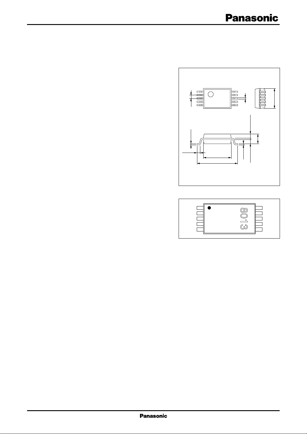
AN8013SH is provided in a 0.5 mm pitch 10-pin surface
mounting package and is optimal for use in miniature
high-efficiency portable power supplies.
0.5±0.2
Unit: mm
1
5
0.5
0.1±0.1
4.3±0.30
6.3±0.30
10
0.2±0.1
6
0.625±0.100.625±0.10
+0.1
–0.05
0.15
3.0±0.30
1.5±0.2
■ Features
• Wide operating supply voltage range (3.6 V to 34 V)
• Small consumption current (2.4 mA typical)
• Supports control over a wide output frequency range:
20 kHz to 500 kHz.
• Built-in pulse-by-pulse overcurrent protection circuit
(Detection voltage: V
− 100 mV)
CC
• Built-in timer latch short-circuit protection circuit
■ Pin Descriptions
CLM
RT
CT
S.C.P.
DTC
(charge current 1.3 µA typical)
• Incorporating the under-voltage lock-out (U.V.L.O.) circuit
• Built-in reference voltage circuit (Error amplifier reference input: 0.75 V (allowance: ±4%))
• Output block is open-collector (darlington) type.
• High absolute maximum rating of output current (100 mA)
• Duty ratio with small sample-to-sample variations (55% ± 5%).
• Adopts a 0.5-mm lead pitch 10-pin small outline package
SSOP010-P-0225
1
2
3
4
5
■ Applications
• Switching mode power supply units (in portable equipment and other applications)
10
V
CC
9
Out
8
GND
7
IN−
6
FB
1
Page 2
AN8013SH Voltage Regulators
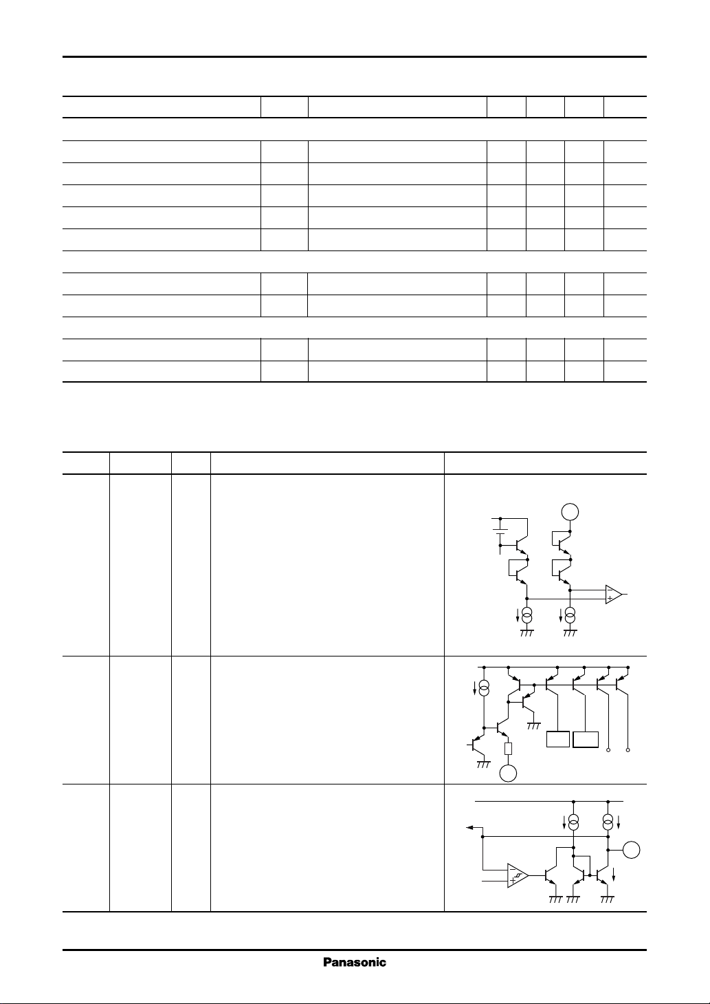
■ Block Diagram
CC
FB
IN−
V
6
Error amp.
7
V
10
REF
0.75 V
0.1 V
CLM
1
S.C.P. comp.
1.90 V
DTC
5
V
REF
R
S R
Latch
V
REF
R
T
4
S.C.P.
T
0.75 V
V
REF
S R
Latch
PWM
R
S Q
U.V.L.O.
CT3RT
2
OSC
9
Out
8
GND
■ Absolute Maximum Ratings at Ta = 25°C
Parameter Symbol Rating Unit
Supply voltage V
CLM pin allowable application voltage V
Error amplifier allowable input voltage V
DTC pin allowable input voltage V
Out pin allowable application voltage V
Collector output current I
Power dissipation (Ta = 85°C) P
Operating ambient temperature T
Storage temperature T
CC
CLM
IN−
DTC
OUT
OUT
D
opr
stg
35 V
35 V
−0.3 to +2.5 V
2.5 V
35 V
100 mA
154 mW
−30 to +85 °C
−55 to +150 °C
■ Recommended Operating Range at Ta = 25°C
Parameter Symbol Min Max Unit
Supply voltage rise time (0 to 3.6 V) tr (VCC)10 µs
Collector output voltage V
Collector output current I
Timing capacitance C
Timing resistance R
Oscillator frequency f
Short-circuit protection time constant setting C
capacitor
OUT
OUT
T
T
OUT
SCP
34 V
50 mA
100 1 800 pF
5.1 15 kΩ
20 500 kHz
1 000 pF
2
Page 3

Voltage Regulators AN8013SH
■ Electrical Characteristics at Ta = 25°C
Parameter Symbol Conditions Min Typ Max Unit
U.V.L.O. block
Circuit operation start voltage V
Hysteresis width V
UON
HYS
Error amplifier block
Input threshold voltage V
Line regulation with input fluctuation V
Voltage follower 0.72 0.75 0.78 m V
TH
Voltage follower, 28mV
dv
VCC = 3.6 V to 34 V
Input bias current I
High-level output voltage V
Low-level output voltage V
Input threshold voltage temperature V
B
EH
EL
Voltage follower, ±1 %
dt1
characteristics 1 Ta = −30°C to +25°C
Input threshold voltage temperature V
Voltage follower, ±1 %
dt2
characteristics 2 Ta = −25°C to +85°C
Output sink current I
Output source current I
SOURCEVFB
Open-loop gain A
VFB = 0.9 V 8 mA
SINK
= 0.9 V −120 µA
V
PWM Comparator Block
Input threshold voltage: high V
Input threshold voltage: low V
Input current I
Duty: 100% 1.2 V
DT-H
Duty: 0% 0.6 V
DT-L
DTC
Output block
Oscillation frequency f
Output duty Du R
Output saturation voltage V
Output leak current I
RT pin voltage V
Maximum oscillation frequency f
OUT(max)RT
Frequency supply voltage f
RT = 15 kΩ, CT = 150 pF 185 205 225 kHz
OUT
= 91 kΩ 50 55 60 %
DTC
OLIO
LEAKVCC
RT
= 50 mA, RT = 15 kΩ0.9 1.2 V
= 34 V, when output Tr is off 10 µA
= 5.1 kΩ, CT = 120 pF 500 kHz
f
dV
= 200 kHz, ±1 %
OUT
characteristics VCC = 3.6 V to 34 V
Frequency temperature f
dT1fOUT
characteristics 1
Frequency temperature f
dT2fOUT
characteristics 2
Note)
At VCC = 12 V, RT = 15 kΩ, CT = 15 pF, unless otherwise specified.
= 200 kHz,
Ta = −30°C to +25°C
= 200 kHz,
Ta = 25°C to 85°C
2.8 3.1 3.4 V
100 200 300 mV
−500 −25 nA
2.0 V
0.3 V
70 dB
−12 −11 −10 A
0.59 V
±3 %
±3 %
3
Page 4
V
CC
CLM
comp.
50 µA50 µA
0.1 V
1
AN8013SH Voltage Regulators
■ Electrical Characteristics at Ta = 25°C (continued)
Parameter Symbol Conditions Min Typ Max Unit
Short-circuit protection circuit block
Input threshold voltage V
Input standby voltage V
Input latch voltage V
Charge current I
Comparator threshold voltage V
THPC
STBY
IN
CHG
THL
V
= 0 V −1.6 −1.3 − 1.0 µA
SCP
Overcurrent Protection Block
Input threshold voltage V
Delay time t
CLM
DLY
Whole device
Total consumption current 1 I
Total consumption current 2 I
Note)
At VCC = 12 V, RT = 15 kΩ, CT = 15 pF, unless otherwise specified.
RT = 15 kΩ2.4 3.5 mA
CC
RT = 5.1 kΩ, CT = 150 pF 3.4mA
CC2
■ Terminal Equivalent Circuits
Pin No. Pin I/O Function Internal equivalent circuit
1 CLM I Detects the overcurrent state in switching
transistor.
Insert a resistor with a low resistance between
this pin and V
When this pin falls to a level 100 mV or more
lower than VCC, the PWM output is turned off
for that period thus narrowing the width of
the on period.
(This implements a pulse-by-pulse
overcurrent protection technique.)
2 RT I Connection for the timing resistor that deter-
mines the oscillator frequency.
Use a resistor in the range 5.1 kΩ to 15 kΩ.
Thus the pin voltage will be about 0.59 V.
3 CT O Connection for the timing capacitor that
determines the oscillator frequency.
Use a capacitor in the range 100 to 1 800 pF.
See the "Application Notes, [2] and [3]"
sections later in this document for details on
setting the frequency. Use an oscillator
frequency in the range 20 kHz to 500 kHz.
to detect overcurrent states.
CC
V
V
To PWM input
0.70 0.75 0.80 V
120 V
120 mV
1.90 V
VCC − 120 VCC − 100 VCC − 80
200 ns
REF
100 Ω
RT (V ≈ 0.59 V)
2
REF
OSC
comp.
OSC PWM
S.C.P.
mV
DTC
2I
I
O
3
O
4
Page 5
Voltage Regulators AN8013SH
■ Terminal Equivalent Circuits (continued)
Pin No. Pin I/O Function Internal equivalent circuit
4 S.C.P. O Connection for the capacitor that determines
the time constant for soft start and the timer
latch short-circuit protection circuit.
Use a capacitor with a value of 1 000 pF or
higher.
The charge current I
is determined by the
CHG
timing resistor RT, and sample-to-sample and
temperature variations can be suppressed.
When R
is 15 kΩ, the current will be about
T
−1.3 µA.
I
CHG
V
=
R
RT
1
×
[A]
30
T
5 DTC I Connection for the resistor and capacitor that
determine the PWM output dead-time and the
soft start period.
The input current I
is determined by the
DTC
timing resistor RT, and sample-to-sample and
temperature variations can be suppressed.
When R
is 15 kΩ, the current will be about
T
−11 µA.
I
CHG
V
=
R
RT
1
×
[A]
3.6
T
6 FB O Error amplifier output
A source current is about −120 mA and a sink
current is about 8 mA.
Correct the gain and the phase frequency
characteristics by inserting a resistor and a
capacitor between this pin and IN−pin.
7IN− I Error amplifier inverting input
For common-mode input, use in the range
− 0.1 V to +0.8 V.
V
REF
U.V.L.O.
V
REF
U.V.L.O.
V
REF
V
REF
I
CHG
0.75 V
Latch
S
R
Q
4
I
DTC
CT
PWM
5
120 µA
8 mA
PWM
C
T
6
8 GND Ground
0.75 V
7
8
5
Page 6

AN8013SH Voltage Regulators
V
REF
9
■ Terminal Equivalent Circuits (continued)
Pin No. Pin I/O Function Internal equivalent circuit
9 Out O Open-collector (darlington) output
The absolute maximum rating for the output
current is 100 mA.
Use with a constant output current under 50
mA.
10 V
CC
Power supply connection
Provide the operating supply voltage in
the range 3.6 V to 34 V.
■ Application Notes
[1] Main characteristics
Error amplifier input threshold voltage temperature
characteristics
0.760
= 12 V
V
CC
Voltage follower
0.758
(V)
TH
0.756
0.754
0.752
Input threshold voltage V
0.750
−40 −20 0 20 40 60 80 100
Ambient temperature Ta (°C)
10
Maximum duty ratio temperature characteristics
60
= 12 V
V
CC
= 200 pF
C
T
= 15 kΩ
R
T
58
(%)
max
56
54
Maximum duty ratio Du
52
−40 −20 0 20 40 60 80 100
Ambient temperature Ta (°C)
Oscillator frequency temperature characteristics Timing capacitance Oscillator frequency
215
210
(kHz)
OUT
205
200
V
CC
= 200 pF
C
T
= 15 kΩ
R
T
= 12 V
Oscillator frequency f
195
−40 −20 0 20 40 60 80 100
Ambient temperature Ta (°C)
1M
(Hz)
OUT
100k
RT = 15 kΩ
RT = 5.1 kΩ
Oscillator frequency f
10k
100 1 000 10 000
Timing capacitance CT (pF)
V
CC
= 25°C
T
a
= 12 V
6
Page 7

Voltage Regulators AN8013SH
■ Application Notes (continued)
[1] Main characteristics (continued)
Input threshold voltage line regulation Total consumption current line regulation
(V)
TH
0.765
0.760
= 25°C
T
a
(mA)
CC
4.0
3.5
RT = 5.1 kΩ
= 25°C
T
a
0.755
0.750
Input threshold voltage V
0.745
0 5 10 15 20 25 30 35
Supply voltage VCC (V)
3.0
2.5
RT = 15 kΩ
Total consumption current I
2.0
0 5 10 15 20 25 30 35
Supply voltage VCC (V)
Timing resistance Total consumption current Timing resistance Output saturation voltage
(V)
OL
Output saturation voltage V
0.85
0.84
0.83
0.82
0.81
VCC = 12 V
= 50 mA
I
O
= 25°C
T
a
3.5
(mA)
CC
3.0
2.5
Total consumption current I
VCC = 12 V
T
= 25°C
a
2.0
4
8 12 16
20
Timing resistance RT (kΩ)
0.80
4 20
8 12 16
Timing resistance RT (kΩ)
7
Page 8

AN8013SH Voltage Regulators
■ Application Notes
[2] Function descriptions
1. Reference voltage block
The reference voltage block is based on a band gap circuit, and outputs a temperature corrected reference
voltage of 2.5 V. This reference voltage is stabilized once the supply voltage exceeds 3.6 V, and is used as the
power supply for the IC itself.
2. Triangular wave generator
This circuit generates a triangular wave with a peak of about 1.45 V and a trough of about 0.35 V using a timing
capacitor connected to the CT pin (pin 3) and a timing resistor connected to the RT pin (pin 2) respectively. The
oscillator frequency can be set to arbitrary value by selecting appropriate values for the external capacitor and
resistor, C
to the IC.
3. Error amplifier
fier that detects and amplifies the DC-DC converter
output voltage, and inputs that signal to a PWM comparator.
internal reference voltage. This level is applied to the
noninverting input.
up by inserting a resistor and capacitor in series
between the error amplifier output pin (pin 6) and the
inverting input pin (pin 7).
formula by connecting a resistor divider to the output
as shown in figure 1.
V
4. Timer latch short-circuit protection circuit
against degradation or destruction if an excessive load or a short circuit of the power supply output continues for
longer than a certain fixed period.
output voltage drops and an error amplifier output level exceeds 1.90 V, this circuit outputs a low level and the
timer circuit starts. This starts charging the external protection circuit delay time capacitor.
the latch circuit latches, the output drive transistors are turned off, and the dead-time is set to 100%.
5. Low input voltage malfunction prevention circuit (U.V.L.O.)
power supply voltage falls during power on or power off.
the supply voltage level. While the supply voltage is rising, this circuit cuts off the output drive transistor until the
reference voltage reaches 3.1 V. It also sets the dead-time to 100%, and at the same time holds the S.C.P. pin (pin
4) at the low level. During the fall time of the power supply voltage, it has hysteresis width of 200 mV and operates
2.9 V or less.
and RT. The triangular wave signal is provided to the inverting input the PWM comparator internally
T
This circuit is an PNP-transistor input error ampli-
A 0.75 V level is created by resistors dividing the
Arbitrary gain and phase compensation can be set
The output voltage V
OUT
= 0.75 ×
R1 + R2
is given by the following
OUT
R
2
V
OUT
R1
R2
Figure 1. Connection method of error amplifier
FB
6
Internal 2.5 V
NF
R
IN−
NF
C
7
R3
0.75 V
R4
reference voltage
Error amp.
PWM
comparator
input
This circuit protects the external main switching element, flywheel diode, choke coil, and other components
The timer latch short-circuit protection circuit detects the output of the error amplifier. If the DC-DC converter
If the error amplifier output does not return to the normal voltage range before that capacitor reaches 0.75 V,
This circuit protects the system against degradation or destruction due to incorrect control operation when the
The low input voltage malfunction prevention circuit detects the internal reference voltage that changes with
8
Page 9

Voltage Regulators AN8013SH
■ Application Notes (continued)
[2] Function descriptions (continued)
6. PWM comparator
The PWM comparator controls the output pulse on-period according to the input voltage. The output transistor
is turned on during periods when the level of the CT pin (pin 3) triangular wave is lower than both of the error
amplifier output (pin 6) and the DTC pin (pin 5) voltage.
The dead-time is set by adding a resistor between the DTC pin and ground.
Additionally, the AN8013SH can provide soft start operation in which the output pulse on-period is gradually
lengthened according to an RC time constant when power is first applied by adding a capacitor in parallel with the
resistor R
7. Overcurrent protection block
Destruction of the main switching device, the flywheel diode, and the choke coil, which are easily damaged
by overcurrents, is prevented by limiting the maximum current that flows in the switching device. This is implemented using the fact that power supply output overcurrents are proportional to the current flowing in the main
switching device (a bipolar transistor).
The AN8013SH detects the current by connecting a resistor with a low resistance between the main switching
device and the V
switching device (a bipolar transistor) is on and the CLM pin voltage reaches V
overcurrent detection threshold voltage, the AN8013SH shuts off the output transistor, thus controlling the main
switching device so that currents in excess of the limit cannot occur. While this control operation is repeated at
each period, once an overcurrent is detected the output transistor is turned off for the remainder of that period and
is not turned on again until the next period. This type of overcurrent protection is called pulse-by-pulse overcurrent
protection.
8. Output block
The output drive transistor is of open-collector type output in which transistors are darlington-connected with
a grounded common emitter. The breakdown voltage of collector output terminal (pin 5) is 34 V and it is possible
to obtain up to 100 mA output current.
DTC
.
pin and monitoring the voltage drop across this resistor at the CLM pin (pin 1). When the main
CC
minus 100 mV, which is the
CC
Triangle wave (CT)
Error amplifier output (FB)
Output transistor collector
waveform (Out)
Overcurrent protection input
(CLM)
Overcurrent detection
1
2
Latch set
Latch circuit set signal
Latch circuit reset signal
3
4
Output off
Latch reset
5
On at the next period
T
: Delay time
DLY
Figure 2. Pulse-by-pulse overcurrent protection operating waveforms
1.4 V
0.4 V
High
Low
V
CC
VCC − 100 mV
High
Low
High
Low
9
Page 10

AN8013SH Voltage Regulators
■ Application Notes (continued)
[3] Triangular wave oscillation circuit
1. Setting the oscillator frequency
The waveform of triangular wave oscillation is obtained by charging and discharging of the constant current
from the external timing capacitor CT which is connected to CT pin (pin 3). The constant current is set by the
I
O
externally attached timing resistor R
The peak value of the wave V
0.35 V typical respectively.
The oscillator frequency f
f
OSC
1
=
t1 + t
=
2
2 × CT × (V
.
T
and the trough value of the wave V
CTH
is obtained by the following formula:
OSC
I
O
− V
CHL
)
CTH
are fixed at about 1.45 V typical and
CTL
V
= 1.4 V typ.
CTH
whereas I
because V
=
f
OSC
2.07 × C
= 1.8 ×
O
CTH
1
− V
T
CTL
× R
V
RT
R
T
= 1.1 V
[Hz]
T
= 1.8 ×
0.59
R
T
t
t
Charging Discharging
2
1
= 0.37 V typ.
V
CTL
T
Figure 3. Triangular wave oscillation waveform
The output frequency f
is equal to f
OUT
since it is PWM-controlled.
OSC
2. Usage notes
This IC uses the constant current given by the timing resistor R
as the bias current of the triangular wave
T
generator and the PWM comparator for consumption current reduction. The total consumption current is about 2.4
mA typical when R
constant output current of 100 mA at the open-collector output, it is necessary to set R
is 15 kΩ, and it increases to about 3.4 mA typical when RT is 5.1 kΩ. In order to obtain the
T
value to 15 kΩ or smaller.
T
It is possible to use the circuit in the recommended operating range of 20 kHz to 500 kHz of the oscillator
frequency. As the AN8013SH is used at increasingly higher frequencies, the amount of overshoot and undershoot
due to the operation delay in the triangular wave oscillator comparator increases, and discrepancies between the
values calculated as described previously and the actual values may occur. See the timing capacitance - oscillator
frequency relationship in the "Application Notes, [1] Main characteristics" section of this document.
Note that this IC can not be used as an IC for slave when the several ICs are operated in parallel synchronous
mode.
[4] Setting the dead-time (maximum duty)
The dead-time is set, as shown in figure 4, by setting the DTC pin (pin 5) voltage, V
has a constant current output set with the resistor R
output duty, Du, and the DTC pin voltage, V
frequency of 200 kHz, the output duty will be 0% at V
, V
is adjusted by adding the external resistor R
T
DTC
, are expressed by the following formulas. For an oscillator
DTC
= 0.45 V, and 100% at V
DTC
DTC
is required here, since the amount of overshoot and undershoot in the triangular wave peak (V
(V
) values depends on the oscillator frequency.
CTL
. Since the DTC pin
DTC
= 1.45 V. However, care
) and minimum
CTH
DTC
. The
10
Page 11

Voltage Regulators AN8013SH
■ Application Notes (continued)
[4] Setting the dead-time (maximum duty) (continued)
CT waveform
DTC
waveform
OUT
waveform
Du
V
t
OFFtON
Off OffOn
t
ON
=
tON + t
V
CTH
=
V
CTH
= I
DTC
× R
DTC
= VRT × [V]
OFF
−V
−V
R
× 100 [%]
DTC
CTL
DTC
DTC
R
T
× 100 [%]
1
×
3.6
V
CTH
V
DTC
V
CTL
V
Example: When f
REF
I
DTC
V
=×[A]
I
DTC
R
CT
RT
T
1
3.6
PWM
FB
DTC
R
DTC
= 200 kHz (RT = 15 kΩ, CT = 150 pF)
OSC
V
≈ 1.45 V (typ.) VRT ≈ 0.59 V (typ.)
CTH
V
≈ 0.35 V (typ.) I
CTL
C
DTC
DTC
Figure 4. Setting the dead-time
Adding the external resistor R
and the capacitor C
DTC
in parallel implements a soft start function that causes
DTC
the output pulse on width to increase gradually when the power supply is started. Use of this function can prevent
DC-DC converter output overshoot.
≈ 11 µA (typ.)
[5] Setting the time constant of the timer latch short-circuit protection circuit
The structural block diagram of protection latch circuit is shown in figure 5. The comparator for short-circuit
protection compares the output of error amplifier V
with the reference voltage of 1.90 V all the time.
FB
When the load conditions of DC-DC converter output are stabilized, there is no fluctuation of error amplifier output,
and the short-circuit protection comparator also keeps the balance. At this moment, the output transistor Q1 is in the
conductive state and the S.C.P. pin is hold to about 30 mV through the clamp circuit.
When the load conditions suddenly change, and high-level signal (1.90 V or higher) is input from the error amplifier
to the non-inverted input of the short-circuit protection comparator, the short-circuit protection comparator outputs
the low-level signal. Since this signal cuts off the output transistor Q1, the S.C.P. pin voltage V
externally connected capacitor C
When the external capacitor C
starts charging according to the following equation :
S
has been charged up to about 0.75 V, it sets the latch circuit, cuts off the output drive
S
is released, and the
PE
transistor by enabling the low input voltage malfunction prevention circuit, and sets the dead-time at 100%.
t
[F]
×
CHG
PE
[V]
C
S
t
PE
×
C
S
VPE = V
STBY
+ I
CHG
0.75 V = 0.03 V + I
t
CHG
PE
×
0.72
CS = I
11
Page 12

AN8013SH Voltage Regulators
■ Application Notes (continued)
[5] Setting the time constant of the timer latch short-circuit protection circuit (continued)
I
is the constant current determined by the oscillation timing resistor RT, and its dispersion and fluctuation with
CHG
temperature are small. I
is expressed in the following equation :
CHO
V
I
=
CHG
VRT is about 0.5 V and I
1
RT
×
[A]
30
R
T
becomes about 1.1 µA at RT = 15 kΩ.
CHO
Once the low input voltage malfunction prevention circuit is enabled, the S.C.P. pin voltage is discharged to about
30 mV but the latch circuit is not reset unless the power is turned off.
I
CHG
FB
IN−
6
7
Error amp.
0.75 V
S.C.P. comp.
1.90 V
Q1
4
S.C.P.
C
S
Q2
0.75 V
S R
Latch
R
U.V.L.O.
PWM comparator input
Output cut-off
Figure 5. Short-circuit protection circuit
V
REF
When the power supply is started, the output appears to be shorted. The error amplifier output goes to the high
state, the S.C.P. pin voltage, V
, is released, and charging starts. The external capacitor value must be set so that DC-
PE
DC converter voltage output starts before the latch circuit in the later stage is set. If the soft start function is used,
special care is required to assure that the start time does not become excessive.
12
Page 13

Voltage Regulators AN8013SH
■ Application Notes (continued)
[6] Timing chart
VCC (0 V→3.6 V)
rise time
(VCC) ≥ 10 [µs]
t
r
3.1 V typ.
Lock-out
release
Supply voltage (V
Internal reference voltage
Error amplifier output (FB)
)
CC
3.6 V
2.5 V
1.90 V
Power supply on
S.C.P. pin voltage
Output transistor
collector waveform
(Out)
Internal reference voltage
Short-circuit protection input threshold level
Comparator threshold level
Dead-time voltage (VDT)
Error amplifier output (FB)
Triangular wave(CT)
Triangular wave (CT)
DTC pin voltage
1.40 V
0.40 V
0.03 V
High
Low
Soft start operation Maximum duty
Figure 6. PWM comparator operation waveform
2.5 V
1.90 V
1.40 V
0.40 V
Output transistor collector waveform
(Out)
S.C.P. pin voltage
Short-circuit protection comparator
output
Figure 7. Short-circuit protection operation waveform
High
Low
0.75 V
0.03 V
t
PE
High
Low
13
Page 14

AN8013SH Voltage Regulators
■ Application Circuit Examples
1. Step-down circuit
In
2. Step-up circuit
In
CC10
V
1
CLM
15 kΩ
Out
9
2
RT
SBD
SBD
150 pF
GND
8
3
CT
62 kΩ
11 kΩ
0.01 µF
150 kΩ
IN−
7
4
S.C.P.
0.033 µF
100 kΩ
0.001µF
FB
6
5
DTC
110 kΩ
Out
+5 V
f = 200 kHz
Du
R
Out
+12 V
max
DTC
= 80%
= 110 kΩ
14
CC
V
10
1
CLM
15 kΩ
Out
9
2
RT
150 pF
GND
8
3
CT
10 kΩ
0.01 µF
IN−
7
4
S.C.P.
0.033 µF
100 kΩ
0.001 µF
FB
6
5
DTC
110 kΩ
f = 200 kHz
= 80%
Du
max
= 110 kΩ
R
DTC
Page 15

Voltage Regulators AN8013SH
■ Application Circuit Examples (continued)
3. On/off circuit example
1) Cutting the power supply line
In
On/off
2) Cutting the IC V
In
On/off
CC
Q2
line
Q2
Q1
Q1
C10
C10
CC
V
10
1
CLM
CC
V
10
Q3
SBD
I
CC
Out
9
2
RT
Q3
SBD
I
CC
Out
9
GND
8
3
CT
GND
8
IN−
7
4
S.C.P.
Standby current ≈ 0 µA
IN−
7
FB
6
5
DTC
FB
6
V
O
V
O
1
CLM
2
RT
3
CT
4
S.C.P.
5
5
DTC
Standby current ≈ 0 µA
4. Usage
Since this IC does not include an on/off circuit, an external circuit must be added to implement a standby function.
If a switch (Q1) is inserted in the power supply line as shown in on/off circuit example 1, the standby current can
be held to 0. In this circuit, a transistor essentially equivalent to the one used for the main switching device (Q3) is
required.
If a switch (Q1) is inserted between the power supply line and the IC V
pin (pin 10) as shown in on/off circuit
CC
example 2, the size of the switching device (Q1) can be reduced. However, the sample-to-sample variations in the Q1
saturation voltage will result in sample-to-sample variations in the overcurrent protection threshold level.
5. Usage Notes
If an external on/off circuit is added, the V
rise time may become excessively steep and the IC internal latch circuit
CC
may be set at that time, causing problems at power supply startup. To avoid such problems, set the value of C10 so that
the V
(pin 10) rise time is at least 10 µs.
CC
15
 Loading...