

Page 1
Voltage Regulators
0.3
(0° to 10°)
(0.15)
10.1±0.3
4.2±0.3
6.5±0.3
18
16 9
1.27
(0.605)
Seating plane Seating plane
0.40±0.25
0.1±0.1 1.5±0.2
AN8011S
2-channel step-down, step-up, or inverting use
DC-DC converter control IC
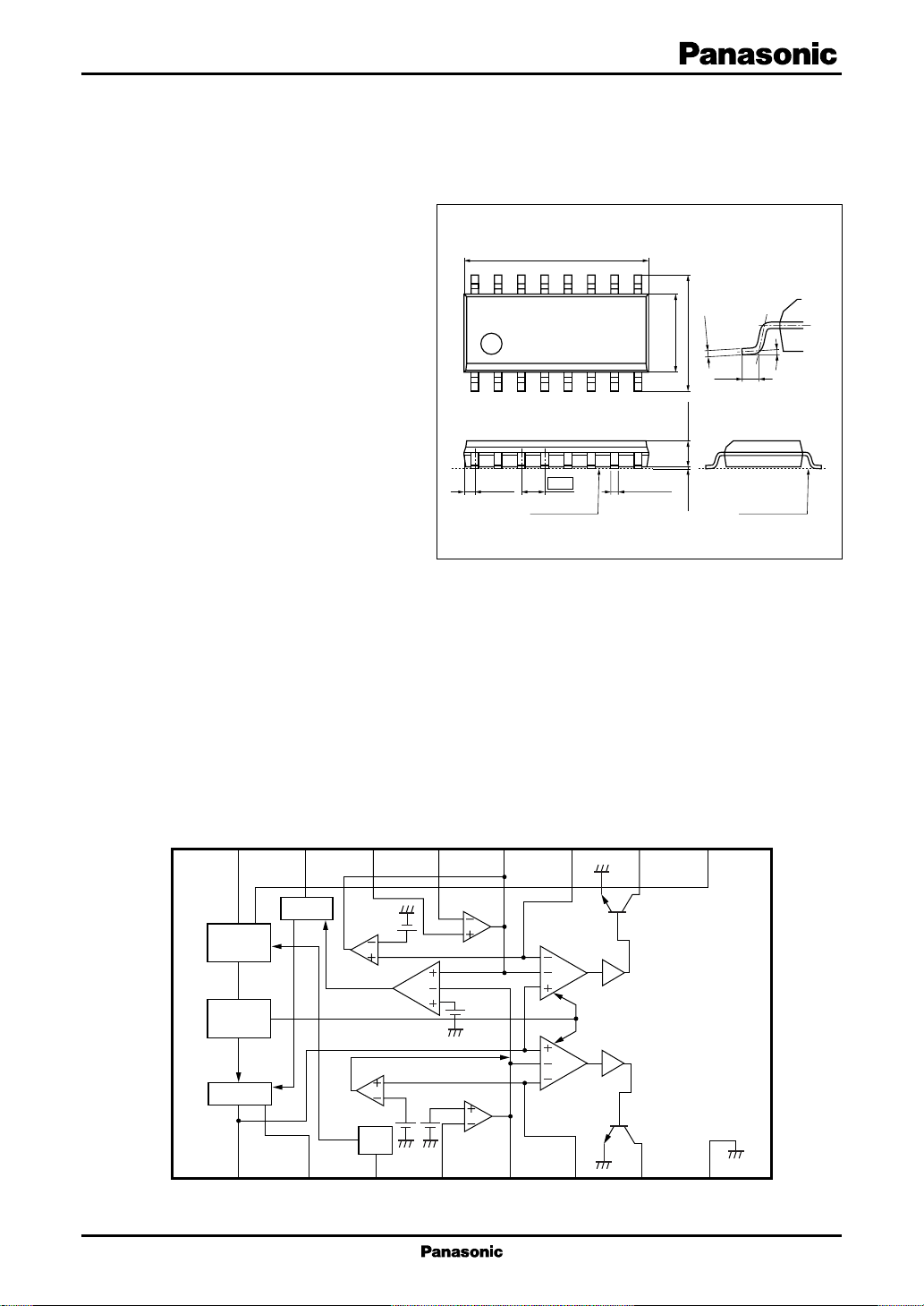
Unit: mm
■ Overview
The AN8011S is a DC-DC converter control IC
with two-channel output using the PWM method
which allows 500 kHz high-speed control.
Respecitve output operation can be completely
synchronized with each other by using the same
oscillation output.
■ Features
• PWM control frequency of 500 kHz is available.
• Wide operating supply voltage range
(V
= 3.6 V to 34 V)
CC
• Built-in 2-channel of open collector type for out-
put (A single-channel is also usable for inverted
amplification type)
• Each output can be stopped independently by the
external control .
• Built-in on/off function for the operation/stop of IC Incorporating circuit for short-circuit portection and under-
voltage lock-out (U.V.L.O.)
• The latch circuit is externally controllable.
• Low consumption current (during operation: 5 mA, during standby: 2 µA)
SOP016-P-0225A
■ Applications
• LCD displays, digital still cameras, and PDAs
■ Block Diagram
REF
V
16
V
REF
U.V.L.O.
OSC
1
CT
Latch
15
Latch
2
RT
IN+
14
Unlatch pro.
Short pro.
Unlatch pro.
On/
Off
3
On/Off
IN−1
13
Error amp.
Error amp.
4
IN−2
12
FB1
5
FB2
11
PWM1
PWM2
6
DTC1
DTC2
10
7
Out1
Out2
9
8
CC
V
GND
1
Page 2

AN8011S Voltage Regulators
■ Pin Descriptions
Pin No. Symbol Description
1 CT Pin for connecting the oscillation frequency setting capacitor for triangular oscillation
circuit. Frequecy of triangular oscillation is set by connecting a capacitor between this
terminal and GND.
2 RT Resistor connection pin for setting the oscillation frequency of triangular oscillation
circuit. Frequecy of triangular oscillation is set by connecting resistance between the
pin and GND
3 On/Off "On/Off" pin for turning on/off IC. "Low" stops IC (output off) and "High" operates IC.
4IN−2 Inverted input pin for channel 2 error amplifier
5 F/B 2 Output pin for channel 2 error amplifier. Gain setting or phase compensation is per-
formed by connecting resistor or capacitor between the pin and IN−2. It is also connected
to PWM short-circuit protecion.
6 DTC 2 Pin for setting dead-time period of channel 2. The dead-time of channel 2 is set by
connecting external resistor. Soft start function can be also given by connecting capacitor in parallel with the external resistor. In addition, only channel 2 output can be turned
off by decreasing the pin voltage to below 0.12 V. (short-circuit protection function stop
circuit)
7 Out 2 Channel 2 open-collector type output pin. IO = 100 mA maximum
8 GND Grounding pin of signal system.
9VCCPower supply voltage application pin. It detects start voltage and stop voltages
10 Out 1 Channel 1 open-collector type output pin. IO = 100 mA maximum
11 DTC 1 Pin for setting dead-time period of channel 1. The dead-time period of channel 1 is set
by connecting external resistor. Soft start function can be also given by connecting capacitor
in parallel with the external resistor. In addition, only channel 1 output can be turned off
by decreasing the pin voltage to below 0.12 V. (short-circuit protection function stop
circuit)
12 F/B 1 Output pin for channel 1 error amplifier. Gain setting or phase compensation is per
formed by connecting resistor or capacitor between the pin and IN−1. It is also con
nected to PWM short-circuit protection.
13 IN−1 Inverted input pin for channel 1 error amplifier.
14 IN+ Pin for noninverted input of channel 1error amplifier.
15 Latch Pin for connecting the time constant setting capacitor for timer latch type short-circuit
protection circuit. The time constant for short-circuit protection is set by connecting
a capacitor between this terminal and GND.
16 V
REF
Internal reference voltage output pin (2.5 V(allowance: ±3%)). If a load of 20 mA typical
or more is applied, the overcurrent protection operates to reduce V
and switching
REF
operation stops.
2
Page 3
Voltage Regulators AN8011S
■ Absolute Maximum Ratings at Ta = 25°C
Parameter Symbol Rating Unit
Supply voltage V
Power dissipation
*
Operating ambient temperature T
Storage temperature T
Note) 1 . Do not apply ecternal currents or voltages to any pins not speifically mentioned.
For circuit currents, '+' denotes current flowing into the IC, and '−' denotes current flowing out of the IC.
2*: When using the IC at Ta of 25°C or more, the power dessipation should be decreased 3.8 mW per 1°C.
CC
P
D
opr
stg
■ Recommended Operating Range
Parameter Symbol Range Unit
Supply voltage V
CC
■ Electrical Characteristics at VCC = 12 V, Ta = 25°C
Parameter Symbol Conditions Min Typ Max Unit
Reference voltage block
Output voltage V
Input regulation with input fluctuation Line VCC = 3.6 V to 34 V 320mV
Load regulation Load I
Output voltage temperature V
characteristics 1
*
Output voltage temperature V
characteristics 2
*
Overcurrent protection drive current *I
U.V.L.O. block
Circuit operation start voltage V
Hysteresis width V
Error amplifier block 1
Input offset voltage 1 V
Input current 1 I
Common-mode input voltage range V
High-level output voltage 1 V
Low-level output voltage 1 V
Error amplifier block 2
Input current 2 I
Common mode input threshold voltage
High-level output voltage 2 V
Low-level output voltage 2 V
REF
= 0 mA to 5 mA 210mV
REF
TC1Ta
TC2Ta
CC
UON
HYS
IN-O1
B1
CM
EH1
EL1
B2
= −25°C to + 25°C ±1 %
= 25°C to 85°C ±1 %
VIN+ 0.72 0.75 0.78 V
EH2
EL2
35 V
380 mW
−30 to +85 °C
−40 to +125 °C
3.6 to 34 V
2.413 2.5 2.588 V
−20 mA
2.8 3.1 3.4 V
100 200 300 mV
−6 6mV
−500 −25 100 nA
0.5 0.8 V
V
− 0.3
REF
V
0.5 V
25 100 nA
V
− 0.3
REF
V
0.5 V
3
Page 4
AN8011S Voltage Regulators
■ Electrical Characteristics(continued) at VCC = 12 V, Ta = 25°C
Parameter Symbol Conditions Min Typ Max Unit
PWM comparator 1/2 block
High-level input threshold voltage V
Low-level input threshold voltage V
Input current I
DT-HfOSC
DT-LfOSC
DTC
Output 1/2 block
Output frequency 1 f
Frequency 1 f
OUT1CT
dv
Output duty ratio 1 Du1CT = 150 pF, RT = 20 kΩ, R
Output duty ratio 2 Du2CT = 150 pF, RT = 20 kΩ, R
Output saturation voltage 1 V
Output saturation voltage 2 V
Output leak current 1 I
Frequency temperature characteristics 1 *f
Frequency temperature characteristics 2 *f
Output frequency 2
Frequency 2
*
*
O(sat)1IO
O(sat)2IO
OLe1
dT1fOSC
dT2fOSC
f
OUT2CT
f
dv2
Short-circuit protection block
Input threshold voltage V
Latch drive voltage V
Charge current
SLTH
SLON
I
CHG
Unlatch pro. 1/2 block
Input threshold voltage V
ULTH
On/off block
Threshold voltage V
TH
Whole device
Total consumption current
Total consumption current fluctuation
Standby consumption current I
Maximum standby consumption current I
Note)*: These characteristics are theoretical values based on the IC design and are not guaranteed.
I
CC
I
CC(max.)VCC
CC(SB)VCC
CC(SB-M)VCC
= 200 kHz, duty = 100% 1.2 V
= 200 kHz, duty = 100% 0.6 V
RT = 20 kΩ−37 −34 −31 µA
= 150 pF, RT = 20 kΩ, IO = 30 mA
180 200 220 kHz
VCC = 3.6 V to 34 V −2 2%
CT = 150 pF, RT = 20 kΩ
DTC
DTC
= 24 k Ω
= 33 k Ω
40 45 50 %
65 75 85 %
= 30 mA 0.9 V
= 100 mA 1.2 V
V
= 34 V, when output 10 µA
CC
transistor is off
= 200 kHz, Ta = −30°C to +25°C
= 200 kHz, Ta = 25°C to 85°C
= 150 pF, RT = 6.6 kΩ, IO = 30 mA
±9 %
±9 %
500 kHz
VCC = 3.6V to 34V, ±2 %
CT = 150 pF, RT = 6.6 kΩ
1.75 1.85 1.95 V
1.15 1.25 1.35 V
−120 −50 −40 µA
0.12 V
0.8 2V
VCC = 12 V, RT = 20 kΩ57mA
= 3.6 V to 34 V, RT = 20 kΩ 2mA
= 12 V, V
= 34 V, V
is down 2 µA
REF
is down 5 µA
REF
4
Page 5
Voltage Regulators AN8011S
■ Terminal Equivalent Circuits
Pin No. Equivalent circuit Description I/O
1 CT: O
V
REF
16
To PWM input
OSC
comp.
2 RT: I
V
REF
16
OSC PWM
The terminal used for connecting a timing
capacitor to set oscillator frequency. Use a
I
O
capacitance value within the range of 100 pF
CT
to 0.1mF. For frequency setting method, re-
1
fer to the "Application Notes, [2] Function
descriptions" section. Use the oscillation fre-
2I
O
quency in the range of 1 kHz to 500 kHz.
The terminal used for connecting a timing
resistor to set oscillattion frequency.
Use a resistance value ranging from 5.1 kΩ
to 20 kΩ.
The terminal voltage is 0.67 V typ.
RT (= 0.67 V)
2
3 On/Off: I
The terminal for on/off control.
High-level input: normal operation
(V
ON/OFF
> 2.0 V typ.)
Low-level input: standby state
(V
ON/OFF
< 0.8 V typ.)
On/Off
3
Internal
circuit start/stop
17 kΩ
13 kΩ
The total current consumption in the standby
state can be suppressed to a value below 5 µA.
4IN−2: I
V
REF
16
The terminal for the inverted input of ch.2
error amplifier. Use a common-mode input
ranging from − 0.1 V to 0.8 V.
0.75 V
4
IN−2
5
Page 6

AN8011S Voltage Regulators
■ Terminal Equivalent Circuits (continued)
Pin No. Equivalent circuit Description I/O
5 FB2: O
6 DTC2: I
7 Out2: O
V
V
V
REF
REF
REF
U.V.L.O.
output
16
16
16
I
DTC2
6
8 mA
typ.
DTC2
25 µA typ.
CT
5
FB2
CT
PWM2
PWM2
Out2
7
The output terminal of ch.2 error amplifier.
Its source current is −25 µA typ. and sink
current is 8 mA typ.
Correct the frequency characteristics of the
gain and the phase by connecting a resistor
and a capacitor between the terminal and
IN−2 terminal.
1) Terminal for connecting a resistor and a
capacitor for setting the dead-time and the
soft start period of ch.2 PWM output.
Input current I
is determined by the tim-
DTC
ing resistor RT so that dispersion, and fluctuation with temperature are suppressed. The
input current is −35 µA typ.
when R
I
R
DTC2
=
T
VRT
= 20 kΩ
× 1.04 (A)
T
(VRT: 0.67 V typ.)
2) The ch.2 output can be turned off by reducing the terminal voltage to below 0.12 V.
(short-circuit protection function stop)
The ch.2 open-collector type (Darlington)
output terminal.
The absolute maximum rating of ouput current is 150 mA.
Use with an output current under 100 mA
normally.
8 GND:
8
GND
9V
9
V
CC
GND pin
:
CC
The pin to which supply voltage is applied.
Use within an operating supply voltage range
of 3.6 V to 34 V.
6
Page 7

Voltage Regulators AN8011S
■ Terminal Equivalent Circuits (continued)
Pin No. Equivalent circuit Description I/O
10 Out1: O
V
REF
16
11 DTC1: I
V
REF
16
I
DTC1
U.V.L.O.
output
11
12 FB1: O
V
REF
16
CT
DTC1
25 µA typ.
CT
8 mA
typ.
12
FB1
Out1
10
PWM1
PWM1
The ch.1 open collector type (darlington)
output terminal.
The absolute maximum rating of output current is 150 mA.
Use with an output current of 100 mA or less
normally.
1) Terminal for connecting a resistor and a
capacitor for setting the dead-time and the soft
start period of ch.1 PWM output.
Input current I
is determined by the tim-
DTC
ing resistor RT so that dispersion and fluctuation with temperature are suppressed. The
input current is −35 µA typ, when R
VRT
I
=
DTC2
R
× 1.04 (A)
T
(VRT: 0.67 V typ.)
= 20 kΩ.
T
2) The ch.1 output can be turned off by reducing the terminal voltage to below 0.12 V.
(short-circuit protection function stop)
The output terminal of ch.1 error amplifier.
Its source current is −25 µA typ. and sink
current is 8 mA typ.
Correct the frequency characteristics of the
gain and the phase by connecting a resistor
and a capacitor between the terminal and
IN−1 terminal.
13 IN−1: I
V
REF
The terminal for the inverted input of ch.1
error amplifier. Use a common-mode input
ranging from − 0.1 V to +0.8 V.
14 IN+:I
The terminal for noninverted input of ch.1
13
IN − 1
14
IN +
error amplifier. Use a common-mode input
ranging from − 0.1 V to +0.8 V.
7
Page 8

AN8011S Voltage Regulators
■ Terminal Equivalent Circuits (continued)
Pin No. Equivalent circuit Description I/O
15 Latch: O
V
REF
16
I
CHG
4.2 kΩ
typ.
10kΩ
typ.
30 kΩ
typ.
1.25 V
typ.
Latch
S
R
Q
Terminal for connecting the time constant
setting capacitor for timer latch short-circuit
protection circuit. The charge current I
CHG
is
about −80 µA.
1.25 V
typ.
15
Latch
16 V
V
CC
9
V
overcurrent
REF
detection
Bias to
other blocks
V
16
REF
:O
REF
The output terminal for the reference voltage
(2.5 V typ.).
Use it with a load current of −1 mA or under.
The terminal has a built-in short-circuit protection circuit, and the short-circuit current
is −20 mA typ.
Use the terminal for setting the reference input of the error amplifier.
8
Page 9

Voltage Regulators AN8011S
■ Application Notes
[1] Main characteristics
Reference voltage temperature characteristics Maximum duty ratio temperature characteristics
2.500
54
2.495
(V)
REF
2.490
2.485
Reference voltage V
2.480
−20 0 20 40 60 80
−40 100
Ambient temperature Ta (°C)
53
52
51
50
Maximum duty ratio Du(45) (%)
49
−20 0 20 40 60 80
−40 100
Ambient temperature Ta (°C)
Output frequency temperature characteristics DTC pin voltage Output duty ratio
210
209
208
207
(kHz)
OUT
206
205
204
203
Output frequency f
202
201
200
−20 0 20 40 60 80
−40 100
Ambient temperature Ta (°C)
100
90
80
70
60
50
f
= 500 kΩ
40
30
Output duty ratio (%)
20
10
OUT
0
0
f
= 200 kΩ
OUT
0.5 1 1.5
DTC pin voltage (V)
Output frequency characteristics
500
100
(kHz)
Output frequency f
OUT
10
0
10
RT = 10 kΩ
2
R
T
= 20 kΩ
= 5.1 kΩ
R
T
3
10
C
T
(pF)
4
10
5
10
9
Page 10

AN8011S Voltage Regulators
■ Application Notes (continued)
[2] Function descriptions
1. Reference voltage block
This block is composed of the band gap circuit, and outputs the temperature compensated 2.5 V reference
voltage to the V
used as the operating power supply for the IC inside. It is possible to take out a load current of up to −3 mA. Also,
an overcurrent portection circuit is built in for the load, thereby protecting the IC from destruction when V
terminal is short circuited.
2. Triangular wave oscillation block
The triangular wave which swings from the wave peak of approximately 1.4 V to the wave bottom of
approximately 0.4 V will be generated by connecting a timing capacitor and a resistor to the CT terminal and RT
terminal respectively. The oscillation frequency can be freely decided by the value of C
externally. The triagular wave is connected with the inverted input of PWM comparator of the IC inside.
3. Error amplifier block
This block detects the output voltage of DC-DC conveter, and inputs the signal amplified by the PNP transistor
input type differential amplifier to the PWM comparator.
The common-mode input voltage range is − 0.1 V to 0.8 V, and is a voltage obtained by dividing the reference
voltage with resistors.
Also, it is possible to perform the gain setting and the phase compensation arbitrarily by connecting the
feedback resistor and the capacitor from the error amplifier output terminal to the inverted input terminal.
The output voltage V
noninverted input terminal as shown in figure 1. 1), and the output voltage V
connecting to the inverted input terminal as shown in figure 1. 2). The output voltages in each of these cases are
given in the following equations.
V
= VIN ×
OUT1
= V
V
IN+
V
OUT1
R1 R3
R2 R4
terminal. The reference voltage is stabilized when the supply voltage is 3.6 V or higher, and
REF
and RT connected
T
, if positive, is obtained by connecting the resistor-divided reference voltage to the
OUT
, if negative, is obtained by
OUT
REF
V
IN+
IN−1
R1 + R2
R2 R3
R1 + R2
×
R2 R1 + R2
REF
16
Error amp.1 Error amp.1
14
PWM comparator
input
13
R
NF
12
FB1
V
V
OUT1
IN−1
= − (V
= V
REF
V
R1 R3
IN+
IN−1
R2 R4
REF
×
REF
− V
16
14
13
R2
IN-1
R
NF
) ×
R3 + R4
12
PWM comparator
input
FB1
+ V
REF
REF
C
NF
1) Positive output
Figure 1. Connection method of error amplifier 1
The output voltage of channel 2 V
exclusively for positive voltage ouput, and
method of connection is as shown in figure 2.
V
OUT2
= 0.75 ×
R1 + R2
R2
10
OUT2
V
OUT1
C
NF
2) Negative output
is
V
OUT2
R1
FB2
5
NF
NF
C
R
IN−2
R3
0.75V
V
: 2.5 V
REF
Error amp.2
PWM comparator input
4
R2
R4
Figure 2. Cnnection method of error amplifier 2
Page 11

Voltage Regulators AN8011S
■ Application Notes (continued)
[2] Function descriptions (continued)
4. Timer latch short-circuit protection circuit
This circuit protects the external main swiching devices, switching diodes, choke coils, and etc. from
destruction or deterioration if overload or short-circuit of power supply output lasts for a certain time.
The timer latch type short-circuit protection circuit detects the output level of each error amplifier, and when
the ouput level of either one or both of the error amplifiers exceeds 1.85 V typical, the timer circuit is actuated, and
initiates charging the external capacitor for protection enable.
If the ouput of the error amplifier does not return to a normal voltage range by the time when the voltage of
this capacitor reaches 1.25 V, it sets the latch circuit, cuts off the ouput drive transistor, and sets the dead time to
100%.
5. Low input voltage malfunction prevention circuit (U.V.L.O.)
This circuit protects the system from destruction or deterioration due to control malfunction caused by the
supply voltage reduction in the transient state of power on or off.
The low input voltage malfunction prevention circuit detects the internal reference voltage according to the
supply voltage level, and cuts off the output drive transistor by resetting the latch circuit, thereby setting the deadtime to 100% and keeping the latch terminal low.
6. PWM comparator block
The PWM comparators, each has one inverted input, and two noninverted inputs, and controls the on-period
of output pulse in accordance with the input voltage. It turns on the output transistor during the period when the
triangular wave of C
The dead-time is set by the addition of a resistor between the DTC terminal and GND. By the addition of a
capacitor in parallel with the external resistor R
of the ouput pulse by the RC time constant when the power supply is turned on starts to work.
7. Output block
The ouput drive transistor is of open-collector type output connected in Darlington circuit of emitter common
GND. The breakdown voltage of the collector ouput terminal is 34 V and it is possible to obtain up to 100 mA
ouput current.
8. Remote circuit
It is possible to switch on/off the IC control by an external control signal. When the on/off terminal voltage is
lowered to a value below approximately 0.8 V, the internal reference voltage goes down, thereby the IC control
is stopped and the circuit current is decreased to 5 µA or less. When the on/off terminal voltage is increased to a
value higher than approximately 2.0 V, the internal reference voltage raises and the control operation is started.
terminal is lower than either the error amplifier ouput voltage or the DTC terminal voltage.
T
, the soft start function which gradually extends the on-period
DTC
[3] The time constant setting method for timer latch type short-circuit protection circuit
Figure 3 shows the block diagram of the protection latch circuit. The comparator for short-circuit protection
compares the output voltage of error amplifier V
with the reference voltage (1.85 V) at all the time. When the load
FB
conditions of DC-DC converter output is stabilized, there is no fluctuation of error amplifier output, and the shortcircuit protection comparator also keeps the balance. At this moment, the switch SW1 will be in the off state, and the
latch terminal voltage will be kept at approximately 0.9 V typical.
When the load conditions suddenly change, and high-level signal (1.85 V typical of higher) is inputted from the
error amplifier to the noninverted input of the short-circuit protection comparator, the short-circuit protection comparator outputs the high-level signal. This signal turns on the switch SW1, and the charging to the capacitor C
connected externally to the latch terminal is started with a current of 80 µA typical.
When the external capacitor C
is charged up to approximately 1.25 V typical, the latch circuit is set and the under-
S
voltage lock-out circuit (U.V.L.O.) is enabled, thereby the ouput drive transistor is cut off and the dead-time is set to
100%.
Once the under-voltage lock-out circuit (U.V.L.O.) is enabled, the latch circuit will not be reset unless the power
supply is switched off.
S
11
Page 12

AN8011S Voltage Regulators
f
■ Application Notes (continued)
[3] The time constant setting method for timer latch type short-circuit protection circuit (continued)
V
REF
I
CHG
80 µA typ.
5
FB2
Latch comp.
12
FB1
1.85 V
When the power supply is turned on, the output is considered to be short-circuited state, so that the error amplifier
output becomes high-level, then SW1 becomes on state and the charging starts. It is necessary to set the external
capacitor so as to start up the DC-DC converter output voltage before setting the latch circuit in the later stage.
Especially, pay attention to the delay of the start-up time when applying the soft-start.
SW1
30 kΩ
typ.
10 kΩ
typ.
4
4.2 kΩ typ.
1.25 V
typ.
SR
Latch
Latch
C
S
Figure 3. Short-circuit protection circuit
R
Cut output of
U.V.L.O.
[4] Explanation of unlatch protection circuit operation
Figure 4 shows the block diagram of the unlatch protection circuit. It is possible to suppress FB terminal, the error
amplifier output terminal of the channel, to low by setting DTC terminal to 0.12 V or less through external signal.
Consequently, by controlling the DTC terminal voltage, it is possible to operate only one channel, or to start and stop
each channel in any required sequence.
FB1
IN+
IN−1
DTC1
12
14
13
11
Error amp.1
I
DTC1
To PW1
Unlatch protection
comp.1
To PW2
Unlatch protection
comp.2
Error amp.2
I
DTC2
5
4
6
FB2
IN−2
DTC2
0.12 V typ.0.12 V typ.
Figure 4. Unlatch protection circuit
12
Page 13

Voltage Regulators AN8011S
■ Application Notes (continued)
[5] Triangular wave oscillation circuit
• Oscillation frequency setting method
The waveform of triangular wave oscillation is obtained by charging and discharging of the constant current I
from the external timing capacitor CT which is connected to CT terminal. The constant current is set by the externally
attached timing resistor R
The peak value of the wave V
value of the wave V
typical and 0.4 V typical respectively.
The oscillation frequency f
following formula;
1
f
=
OSC
t
(typ.)
Where IO = 2 ×
R
Because V
f
=
OSC
C
(typ.)
=
+ t2 2 × CT × (V
1
VRT
− V
CTH
0.67
× R
T
T
The ouput frequency f
[6] Dead-time (maximum duty) setting method
The setting of the dead-time is conducted by adjusting the DTC terminal voltage V
the DTC terminal provides a constant current output through the resistor R
resistor R
DTC
.
The output duty ratio Du and the DTC terminal voltage V
oscillation frequency f
Pay attention to the peak volue and the trough value of triangular wave because the overshoot and undershoot
voltages depend on the frequency.
.
T
and the trough
CTH
are fixed at approximately 1.4 V
CTL
is obtained by the
OSC
I
T
CTL
O
0.67
= 2 ×
R
= 1V
CTH
− V
)
CHL
T
[Hz]
is equal to f
OUT
is 200 kHz, the output duty ratio is 0% at V
OSC
since it is PWM-controlled.
OSC
V
CTH
= 1.4 V typ.
V
t
1
Charging
t
2
Discharging
CTL
= 0.4 V typ.
T
Figure 5. Triangular wave oscillation waveform
as shown in figure 6. Since
DTC
, V
is adjusted by attaching the external
T
DTC
are expressed by the following formula. When the
DTC
= 0.42 V, and 100% at V
DTC
= 1.35 V.
DTC
O
waveform
C
T
DTC waveform
t
OFF
V
CTH
V
DTC
V
t
ON
CTL
V
I
REF
DTC
I
DTC
=
CT
FB
V
RT
R
× 1.04 [A]
T
PWM
Out waveform
Off OffOn
DTC
t
=
=
= I
= V
ON
tON + t
V
CTH
V
CTH
DTC
×
RT
−V
× R
OFF
−V
R
DTC
CTL
DTC
DTC
R
T
×
100 [%]
×
100 [%]
× 1.04 [V]
ex.) When f
R
DTC
= 200 kHz (RT = 20 kΩ, CT = 150 pF),
OSC
V
≈1.4 V(typ.) VRT≈ 0.67 V(typ.)
CTH
V
≈0.4 V(typ.) I
CTL
C
DTC
DTL
≈ 35 µA (typ.)
Du
(typ.)
V
DTC
(typ.)
Figure 6. Dead-time setting method
When the capacitor C
is added in parallel with the external resistor R
DTC
, the soft start function gradually extends
DTC
the on-period of the output pulse when the power supply is turned on. This prevents the overshoot of the DC-DC
converter output.
13
Page 14

AN8011S Voltage Regulators
■ Application Notes (continued)
[7] Timing chart
3.1 V typ.
Lock-out release
Power supply
on
Dead-time voltage (V
Output transistor collector
waveform(OUT)
DT
Supply voltage (V
Reference voltage (V
Error amplifier output (FB)
Triangular wave (CT)
)
)
CC
)
REF
Latch terminal voltage
Soft start operation Maximum duty
Figure 7. Operation waveform of PWM comparator
3.6 V
2.5 V
1.83 V
1.3 V
0.9 V
0.40 V
0.03 V
High
Low
Reference voltage (V
Short-circuit protection input threshold level
Comparator threshold level
DTC terminal voltage
Latch terminal voltage
Error amplifier ouput (FB)
Triangular wave (CT)
Output transistor collector waveform
(OUT)
Short-circuit protection comparator
output
REF
)
Figure 8. Operation waveform of short-circuit protection
2.5 V
1.85 V
1.4 V
0.9 V
0.40 V
High
Low
t
PE
High
Low
14
Page 15

Voltage Regulators AN8011S
■ Application Circuit Examples
• Application circuit example 1
6 kΩ
14 kΩ
23 kΩ
7 kΩ
REF
V
16
V
REF
U.V.L.O.
OSC
1
150 pF
CT
Latch
15
Latch
2
20 kΩ
Short pro.
RT
On/
Off
IN+
14
3
On/Off
3 V
0.01 µF
120 kΩ
IN−1
13
Error
amp.
Unlatch pro.
Unlatch pro.
Error
amp.
4
IN−2
120 kΩ
0.01 µF
3 V
FB1
12
5
FB2
0.1 µF
PWM1
0.1 µF
DTC1
11
PWM2
6
DTC2
33 kΩ
33 kΩ
V
Out1
10
7
Out2
SBD
CC
SBD
CC
V
9
8
GND
−5 V
f = 200 kHz
Duty = 75%
5V
7
3 V
SBD
5 V
25.5 kΩ
4.5 kΩ
To pin 4
25.5 kΩ
4.5 kΩ
15
Page 16

AN8011S Voltage Regulators
■ Application Circuit Examples
• Application circuit example 2
10 µF
2.5 V
REF
V
16
V
REF
U.V.L.O.
OSC
1
150 pF
CT
Latch
15
Latch
2
20 kΩ
Short pro.
On/
Off
RT
VIN = 7 V
IN+
14
Unlatch pro.
Unlatch pro.
3
On/Off
R
0.01 µF
120 kΩ
IN−1
13
Error
amp.
Error
amp.
4
IN−2
120 kΩ
0.01 µF
VCC = 7 V
FB1
12
5
FB2
0.1 µF
PWM1
PWM2
0.1 µF
500 Ω
500 Ω
DTC1
11
6
DTC2
33 kΩ
Out1
10
7
Out2
33 kΩ
100 Ω
VCC = 7 V
CC
V
9
8
GND
100 Ω
3.3 V
5 V
16
25.5 kΩ
0.75 V
4.5 kΩ
 Loading...