

Page 1
AN79N00 Series
3-pin Negative Output Voltage Regulator (300mA Type)
■ Overview
The AN79N00 series is 3-pin fix ed neg ati ve output v oltage regulators. Stabilized fix ed output volta ge is obtained
from unstable DC input voltage without using an y external components. 12 types of output voltage are available
; –4V, –5V, –6V, –7V, –8V, –9V, –10V, –12V, –15V,
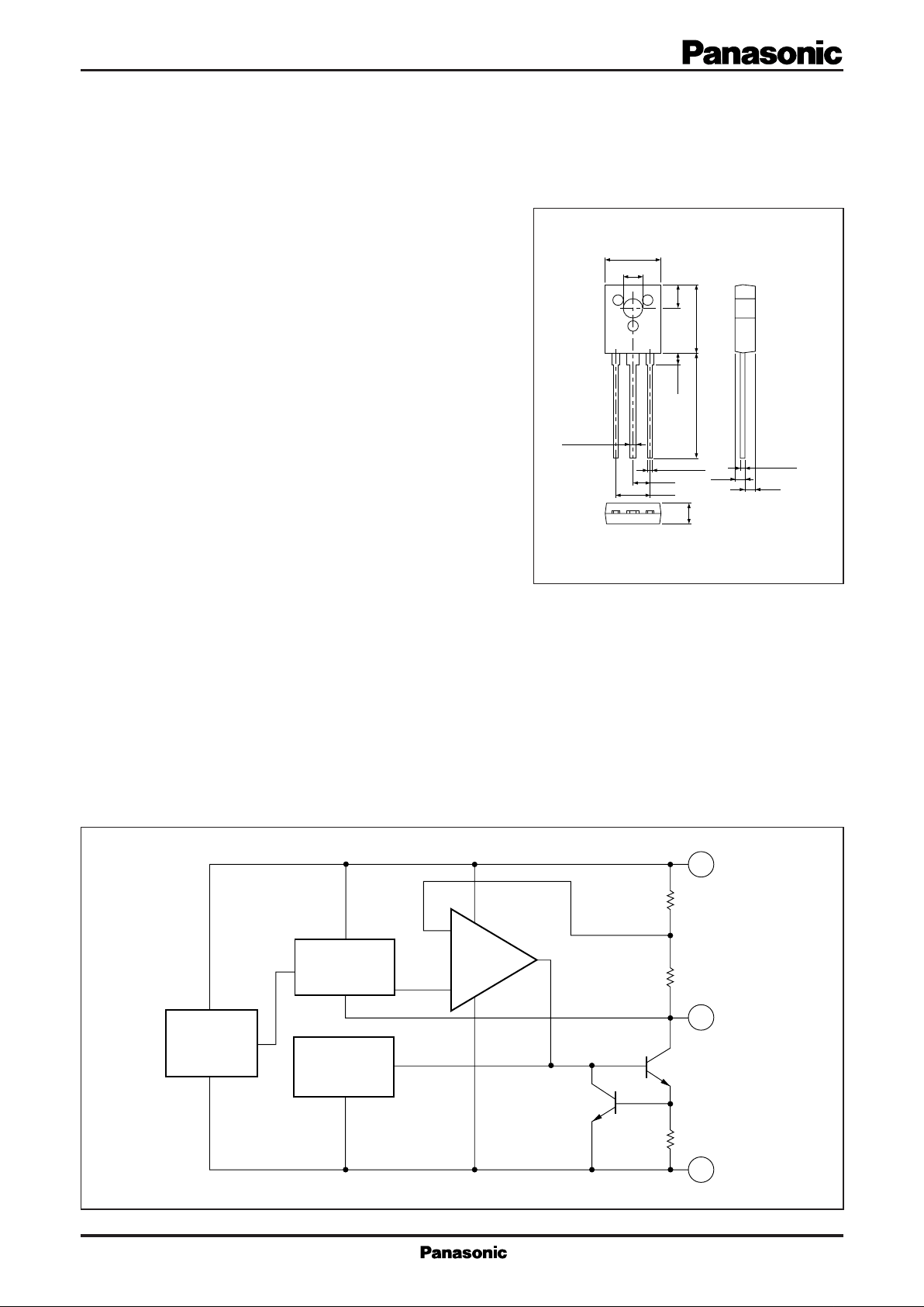
8.0
3.05
+0.5
– 0.1
Unit:mm
3.8
11.5max.15.0min.
–18V, –20V and –24V . They can be used widely in po wer
circuits with current capacitance up to 300mA.
■ Features
• No external components
• Output voltage : –4V, –5V, –6V, –7V, –8V, –9V,
–10V, –12V, –15V, –18V, –20V, –24V
• Short-circuit current limiting built-in
• Thermal overload protection built-in
• Output transistor safe area compensation
■ Block Diagram
1.94
0.75±0.25
0.5±0.25
2.3
4.6
123
JEDEC : TO-126 (SSIP003-P-0000E)
1.44
3.5max.
0.5±0.1
1.76
1 : Common
2 : Input
3 : Output
Starter
Voltage
Reference
Thermal
Protection
+
Error Amp.
–
Current
Limiter
R
R
R
Q
SC
1
2
1
1
3
Pass Tr.
2
Common
Output
Input
Page 2
■ Absolute Maximum Ratings (Ta=25˚C)
Parameter Symbol Rating Unit
1
*
Input voltage
Power dissipation
Operating ambient temperature
Storage temperature
*
1 AN79N04, AN79N05, AN79N06, AN79N07, AN79N08, AN79N09, AN79N10, AN79N12, AN79N15, AN79N18
*
2 AN79N20, AN79N24
*
3 Follow the derating curve, When T
exceeds 150˚C, the internal circuit cuts off the output.
j
V
I
P
D
T
opr
T
stg
–35
2
*
–40
3
*
8
–20 to +80
–55 to +150
V
V
W
˚C
˚C
■ Electrical Characteristics (Ta=25˚C)
AN79N04 (–4V Type)
·
Parameter Symbol Condition min typ max
Output voltage
Output voltage tolerance
Line regulation
Load regulation
Bias current
Input bias current fluctuation
Load bias current fluctuation
Output noise voltage
Ripple rejection ratio
Minimum input/output voltage difference
Output short circuit current
Peak output current
Output voltage temperature coefficient
V
V
REG
REG
I
∆I
Bias (IN)
∆I
Bias (L)
V
RR
V
DIF (min.)
I
O (Short)
I
O (Peak)
∆V
Bias
O
O
O
IN
L
no
/Ta
=25˚C
T
j
VI=–
6 to –25V, IO=5 to 200mA
=–6 to –25V, Tj=25˚C
V
I
=–7 to –17V, Tj=25˚C
V
I
=1 to 300mA, Tj=25˚C
I
O
=5 to 200mA, Tj=25˚C
I
O
=25˚C
T
j
=–7 to –25V, Tj=25˚C
V
I
=5 to 200mA, Tj=25˚C
I
O
f=10Hz to 100kHz
=–7 to –17V, IO=50mA,
V
I
f=120Hz
=200mA, Tj=25˚C
I
O
=–35V, Tj=25˚C
V
I
Tj=25˚C
=5mA
I
O
–3.84
–3.8
60
–4.16 V–4
–4.2
4
10
Note 1) The specified condition Tj=25˚C means that the test should be carried out with the test time so short (within 10ms) that the
drift in characteristic value due to the rise in chip junction temperature can be ignored.
Note 2) When not specified, VI=–9V, IO=100mA, CI=2µF, CO=1µF and Tj=0 to 125˚C
40 mV9
20
80
40
0.5
0.1
Unit
mV
mV20
mV
mA3
5
mA
mA
µV100
mA10
mA500
mV/˚C– 0.4
V
dB
V1.1
Page 3
■ Electrical Characteristics (Ta=25˚C)
AN79N05 (–5V Type)
·
Parameter Symbol Condition min typ max
Output voltage
Output voltage tolerance
Line regulation
Load regulation
Bias current
Input bias current fluctuation
Load bias current fluctuation
Output noise voltage
Ripple rejection ratio
Minimum input/output voltage difference
Output short circuit current
Peak output current
Output voltage temperature coefficient
Note 1) The specified condition T
=25˚C means that the test should be carried out with the test time so short (within 10ms) that the
j
drift in characteristic value due to the rise in chip junction temperature can be ignored.
Note 2) When not specified, VI=–10V, IO=100mA, CI=2µF, CO=1µF and Tj=0 to 125˚C
V
V
REG
REG
I
Bias
∆I
Bias (IN)
∆I
Bias (L)
V
RR
V
DIF (min.)
I
O (Short)
I
O (Peak)
O
O
Tj=25˚C
VI=–
7 to –25V, IO=5 to 200mA
VI=–7 to –25V, Tj=25˚C
IN
L
=–8 to –18V, Tj=25˚C
V
I
I
=1 to 300mA, Tj=25˚C
O
IO=5 to 200mA, Tj=25˚C
T
=25˚C
j
VI=–8 to –25V, Tj=25˚C
IO=5 to 200mA, Tj=25˚C
no
f=10Hz to 100kHz
=–8 to –18V, IO=50mA,
V
I
f=120Hz
=200mA, Tj=25˚C
I
O
=–35V, Tj=25˚C
V
I
Tj=25˚C
I
=5mA
O
–4.8
–4.75
60
10
125
– 0.4
Unit
–5.2 V–5
–5.25
V
50 mV10
5
30
100
50
0.5
0.1
mV
mV20
mV
mA3
5
mA
mA
µV
dB
V1.1
mA10
mA500
mV/˚C∆VO/Ta
AN79N06 (–6V Type)
·
Parameter Symbol Condition min typ max
Output voltage
Output voltage tolerance
Line regulation
Load regulation
Bias current
Input bias current fluctuation
Load bias current fluctuation
Output noise voltage
Ripple rejection ratio
Minimum input/output voltage difference
Output short circuit current
Peak output current
Output voltage temperature coefficient
Note 1) The specified condition T
=25˚C means that the test should be carried out with the test time so short (within 10ms) that the
j
REG
REG
I
∆I
Bias (IN)
∆I
V
RR
V
DIF (min.)
I
O (Short)
I
O (Peak)
V
O
V
O
Bias
Bias (L)
no
/Ta
O
Tj=25˚C
VI=–
8 to –25V, IO=5 to 200mA
VI=–8 to –25V, Tj=25˚C
IN
L
=–9 to –19V, Tj=25˚C
V
I
I
=1 to 300mA, Tj=25˚C
O
IO=5 to 200mA, Tj=25˚C
T
=25˚C
j
=–9 to –25V, Tj=25˚C
V
I
=5 to 200mA, Tj=25˚C
I
O
f=10Hz to 100kHz
=–9 to –19V, IO=50mA,
V
I
f=120Hz
I
=200mA, Tj=25˚C
O
VI=–35V, Tj=25˚C
Tj=25˚C
=5mA
I
O
drift in characteristic value due to the rise in chip junction temperature can be ignored.
Note 2) When not specified, VI=–11V, IO=100mA, CI=2µF, CO=1µF and Tj=0 to 125˚C
–5.75
–5.7
60
10
150
– 0.4
Unit
–6.25 V–6
–6.3
V
60 mV11
6
40
120
60
0.5
0.1
mV
mV20
mV
mA3
5
mA
mA
µV
dB
V1.1
mA10
mA500
mV/˚C∆V
Page 4

■ Electrical Characteristics (Ta=25˚C)
AN79N07 (–7V Type)
·
Parameter Symbol Condition min typ max
Output voltage
Output voltage tolerance
Line regulation
Load regulation
Bias current
Input bias current fluctuation
Load bias current fluctuation
Output noise voltage
Ripple rejection ratio
Minimum input/output voltage difference
Output short circuit current
Peak output current
Output voltage temperature coefficient
Note 1) The specified condition T
=25˚C means that the test should be carried out with the test time so short (within 10ms) that the
j
drift in characteristic value due to the rise in chip junction temperature can be ignored.
Note 2) When not specified, VI=–12V, IO=100mA, CI=2µF, CO=1µF and Tj=0 to 125˚C
REG
REG
I
∆I
Bias (IN)
∆I
V
RR
V
DIF (min.)
I
O (Short)
I
O (Peak)
V
O
V
O
Bias
Bias (L)
no
/Ta
O
Tj=25˚C
VI=–
9 to –25V, IO=5 to 200mA
VI=–9 to –25V, Tj=25˚C
IN
L
=–10 to –20V, Tj=25˚C
V
I
I
=1 to 300mA, Tj=25˚C
O
IO=5 to 200mA, Tj=25˚C
T
=25˚C
j
=–10 to –25V, Tj=25˚C
V
I
=5 to 200mA, Tj=25˚C
I
O
f=10Hz to 100kHz
=–10 to –20V, IO=50mA,
V
I
f=120Hz
=200mA, Tj=25˚C
I
O
VI=–35V, Tj=25˚C
Tj=25˚C
=5mA
I
O
–6.7
–6.65
59
10
175
– 0.5
Unit
–7.3 V–7
–7.35
V
70 mV12
7
35
140
70
0.5
0.1
mV
mV20
mV
mA3
5
mA
mA
µV
dB
V1.1
mA10
mA500
mV/˚C∆V
AN79N08 (–8V Type)
·
Parameter Symbol Condition min typ max
Output voltage
Output voltage tolerance
Line regulation
Load regulation
Bias current
Input bias current fluctuation
Load bias current fluctuation
Output noise voltage
Ripple rejection ratio
Minimum input/output voltage difference
Output short circuit current
Peak output current
Output voltage temperature coefficient
Note 1) The specified condition T
=25˚C means that the test should be carried out with the test time so short (within 10ms) that the
j
V
V
REG
REG
I
∆I
Bias (IN)
∆I
Bias (L)
RR
V
DIF (min.)
I
O (Short)
I
O (Peak)
Bias
O
O
O
IN
L
no
/Ta
=25˚C
T
j
VI=–
10.5 to –25V, IO=5 to 200mA
VI=–10.5 to –25V, Tj=25˚C
=–11 to –21V, Tj=25˚C
V
I
I
=1 to 300mA, Tj=25˚C
O
IO=5 to 200mA, Tj=25˚C
T
=25˚C
j
=–10.5 to –25V, Tj=25˚C
V
I
=5 to 200mA, Tj=25˚C
I
O
f=10Hz to 100kHz
=–11.5 to –21.5V,
V
I
I
=50mA,f=120Hz
O
I
=200mA, Tj=25˚C
O
VI=–35V, Tj=25˚C
Tj=25˚C
=5mA
I
O
drift in characteristic value due to the rise in chip junction temperature can be ignored.
Note 2) When not specified, VI=–14V, IO=100mA, CI=2µF, CO=1µF and Tj=0 to 125˚C
–7.7
–7.6
59
10
200V
– 0.6
Unit
–8.3 V–8
–8.4
V
80 mV13
8
40
160
80
0.5
0.1
mV
mV25
mV
mA3
5
mA
mA
µV
dB
V1.1
mA10
mA500
mV/˚C∆V
Page 5

■ Electrical Characteristics (Ta=25˚C)
AN79N09 (–9V Type)
·
Parameter Symbol Condition min typ max Unit
Output voltage
Output voltage tolerance
Line regulation
Load regulation
Bias current
Input bias current fluctuation
Load bias current fluctuation
Output noise voltage
Ripple rejection ratio
Minimum input/output voltage difference
Output short circuit current
Peak output current
Output voltage temperature coefficient
Note 1) The specified condition T
=25˚C means that the test should be carried out with the test time so short (within 10ms) that the
j
REG
REG
I
∆I
Bias (IN)
∆I
RR
V
DIF (min.)
I
O (Short)
I
O (Peak)
V
O
V
O
Bias
Bias (L)
no
/Ta
O
drift in characteristic value due to the rise in chip junction temperature can be ignored.
Note 2) When not specified, VI=–15V, IO=100mA, CI=2µF, CO=1µF and Tj=0 to 125˚C
Tj=25˚C
VI=–
11.5 to –26V, IO=5 to 200mA
VI=–11.5 to –26V, Tj=25˚C
IN
L
=–12 to –22V, Tj=25˚C
V
I
I
=1 to 300mA, Tj=25˚C
O
IO=5 to 200mA, Tj=25˚C
T
=25˚C
j
=–11.5 to –26V, Tj=25˚C
V
I
=5 to 200mA, Tj=25˚C
I
O
f=10Hz to 100kHz
=–12 to –22V, IO=50mA,
V
I
f=120Hz
=200mA, Tj=25˚C
I
O
VI=–35V, Tj=25˚C
Tj=25˚C
=5mA
I
O
–8.65
–8.55
58
10
225V
– 0.6
–9.35 V–9
–9.45
V
80 mV14
9
50
180
90
0.5
0.1
mV
mV25
mV
mA3
5
mA
mA
µV
dB
V1.1
mA10
mA500
mV/˚C∆V
AN79N10 (–10V Type)
·
Parameter Symbol Condition min typ max Unit
Output voltage
Output voltage tolerance
Line regulation
Load regulation
Bias current
Input bias current fluctuation
Load bias current fluctuation
Output noise voltage
Ripple rejection ratio
Minimum input/output voltage difference
Output short circuit current
Peak output current
Output voltage temperature coefficient
Note 1) The specified condition T
=25˚C means that the test should be carried out with the test time so short (within 10ms) that the
j
V
V
REG
REG
I
∆I
Bias (IN)
∆I
Bias (L)
RR
V
DIF (min.)
I
O (Short)
I
O (Peak)
Bias
O
O
O
no
T
=25˚C
j
VI=–
12.5 to –27V, IO=5 to 200mA
VI=–12.5 to –27V, Tj=25˚C
IN
L
=–13 to –23V, Tj=25˚C
V
I
I
=1 to 300mA, Tj=25˚C
O
IO=5 to 200mA, Tj=25˚C
T
=25˚C
j
=–12.5 to –27V, Tj=25˚C
V
I
=5 to 200mA, Tj=25˚C
I
O
f=10Hz to 100kHz
=–13 to –23V,
V
I
=50mA,f=120Hz
I
O
I
=200mA, Tj=25˚C
O
VI=–35V, Tj=25˚C
Tj=25˚C
=5mA
I
/Ta
O
drift in characteristic value due to the rise in chip junction temperature can be ignored.
Note 2) When not specified, VI=–16V, IO=100mA, CI=2µF, CO=1µF and Tj=0 to 125˚C
–9.6
–9.5
58
10
10
250V
– 0.7
–10.4 V–10
–10.5
80 mV15
50
200
100
0.5
0.1
V
mV
mV25
mV
mA3.0
5
mA
mA
µV
dB
V1.1
mA10
mA500
mV/˚C∆V
Page 6

■ Electrical Characteristics (Ta=25˚C)
AN79N12 (–12V Type)
·
Parameter Symbol Condition min typ max Unit
Output voltage
Output voltage tolerance
Line regulation
Load regulation
Bias current
Input bias current fluctuation
Load bias current fluctuation
Output noise voltage
Ripple rejection ratio
Minimum input/output voltage difference
Output short circuit current
Peak output current
Output voltage temperature coefficient
Note 1) The specified condition T
=25˚C means that the test should be carried out with the test time so short (within 10ms) that the
j
REG
REG
I
∆I
Bias (IN)
∆I
RR
V
DIF (min.)
I
O (Short)
I
O (Peak)
V
O
V
O
Bias
Bias (L)
no
/Ta
O
drift in characteristic value due to the rise in chip junction temperature can be ignored.
Note 2) When not specified, VI=–19V, IO=100mA, CI=2µF, CO=1µF and Tj=0 to 125˚C
Tj=25˚C
VI=–
14.5 to –30V, IO=5 to 200mA
VI=–14.5 to –30V, Tj=25˚C
IN
L
=–15 to –25V, Tj=25˚C
V
I
I
=1 to 300mA, Tj=25˚C
O
IO=5 to 200mA, Tj=25˚C
T
=25˚C
j
=–14.5 to –30V, Tj=25˚C
V
I
=5 to 200mA, Tj=25˚C
I
O
f=10Hz to 100kHz
=–15 to –25V, IO=50mA,
V
I
f=120Hz
=200mA, Tj=25˚C
I
O
VI=–35V, Tj=25˚C
Tj=25˚C
=5mA
I
O
–11.5
–11.4
57
10
10
300V
– 0.8
–12.5 V–12
–12.6
80 mV15
50
240
120
0.5
0.1
V
mV
mV25
mV
mA3
5
mA
mA
µV
dB
V1.1
mA10
mA500
mV/˚C∆V
AN79N15 (–15V Type)
·
Parameter Symbol Condition min typ max Unit
Output voltage
Output voltage tolerance
Line regulation
Load regulation
Bias current
Input bias current fluctuation
Load bias current fluctuation
Output noise voltage
Ripple rejection ratio
Minimum input/output voltage difference
Output short circuit current
Peak output current
Output voltage temperature coefficient
Note 1) The specified condition T
=25˚C means that the test should be carried out with the test time so short (within 10ms) that the
j
REG
REG
I
∆I
Bias (IN)
∆I
RR
V
DIF (min.)
I
O (Short)
I
O (Peak)
V
O
V
O
Bias
Bias (L)
no
/Ta
O
T
=25˚C
j
VI=–
17.5 to –30V, IO=5 to 200mA
VI=–17.5 to –30V, Tj=25˚C
IN
L
=–18 to –28V, Tj=25˚C
V
I
I
=1 to 300mA, Tj=25˚C
O
IO=5 to 200mA, Tj=25˚C
T
=25˚C
j
=–17.5 to –30V, Tj=25˚C
V
I
=5 to 200mA, Tj=25˚C
I
O
f=10Hz to 100kHz
=–18 to –28V, IO=50mA,
V
I
f=120Hz
I
=200mA, Tj=25˚C
O
VI=–35V, Tj=25˚C
Tj=25˚C
=5mA
I
O
drift in characteristic value due to the rise in chip junction temperature can be ignored.
Note 2) When not specified, VI=–23V, IO=100mA, CI=2µF, CO=1µF and Tj=0 to 125˚C
–14.4
–14.25
56
11
10
375V
–0.9
–15.6 V–15
–15.75
80 mV16
50
240
120
0.5
0.1
V
mV
mV25
mV
mA3
5
mA
mA
µV
dB
V1.1
mA10
mA500
mV/˚C∆V
Page 7

■ Electrical Characteristics (Ta=25˚C)
AN79N18 (–18V Type)
·
Parameter Symbol Condition min typ max Unit
Output voltage
Output voltage tolerance
Line regulation
Load regulation
Bias current
Input bias current fluctuation
Load bias current fluctuation
Output noise voltage
Ripple rejection ratio
Minimum input/output voltage difference
Output short circuit current
Peak output current
Output voltage temperature coefficient
Note 1) The specified condition T
=25˚C means that the test should be carried out with the test time so short (within 10ms) that the
j
REG
REG
I
∆I
Bias (IN)
∆I
RR
V
DIF (min.)
I
O (Short)
I
O (Peak)
V
O
V
O
Bias
Bias (L)
no
/Ta
O
drift in characteristic value due to the rise in chip junction temperature can be ignored.
Note 2) When not specified, VI=–27V, IO=100mA, CI=2µF, CO=1µF and Tj=0 to 125˚C
Tj=25˚C
VI=–
21 to –33V, IO=5 to 200mA
VI=–21 to –33V, Tj=25˚C
IN
L
=–21 to –32V, Tj=25˚C
V
I
I
=1 to 300mA, Tj=25˚C
O
IO=5 to 200mA, Tj=25˚C
T
=25˚C
j
=–21 to –33V, Tj=25˚C
V
I
=5 to 200mA, Tj=25˚C
I
O
f=10Hz to 100kHz
=–22 to –32V, IO=50mA,
V
I
f=120Hz
=200mA, Tj=25˚C
I
O
VI=–35V, Tj=25˚C
Tj=25˚C
=5mA
I
O
–17.3
–17.1
55
–18.7 V–18
–18.9
V
80 mV18
13
50
300
10
150
0.5
0.1
450V
mV
mV30
mV
mA3
5
mA
mA
µV
dB
V1.1
mA10
mA500
–1
mV/˚C∆V
AN79N20 (–20V Type)
·
Parameter Symbol Condition min typ max Unit
Output voltage
Output voltage tolerance
Line regulation
Load regulation
Bias current
Input bias current fluctuation
Load bias current fluctuation
Output noise voltage
Ripple rejection ratio
Minimum input/output voltage difference
Output short circuit current
Peak output current
Output voltage temperature coefficient
Note 1) The specified condition T
=25˚C means that the test should be carried out with the test time so short (within 10ms) that the
j
V
V
REG
REG
I
∆I
Bias (IN)
∆I
Bias (L)
RR
V
DIF (min.)
I
O (Short)
I
O (Peak)
Bias
O
O
O
no
/Ta
T
=25˚C
j
VI=–
23 to –35V, IO=5 to 200mA
VI=–23 to –35V, Tj=25˚C
IN
L
=–24 to –34V, Tj=25˚C
V
I
I
=1 to 300mA, Tj=25˚C
O
IO=5 to 200mA, Tj=25˚C
T
=25˚C
j
=–23 to –35V, Tj=25˚C
V
I
=5 to 200mA, Tj=25˚C
I
O
f=10Hz to 100kHz
=–24 to –34V, IO=50mA,
V
I
f=120Hz
=200mA, Tj=25˚C
I
O
VI=–35V, Tj=25˚C
Tj=25˚C
=5mA
I
O
drift in characteristic value due to the rise in chip junction temperature can be ignored.
Note 2) When not specified, VI=–29V, IO=100mA, CI=2µF, CO=1µF and Tj=0 to 125˚C
–19.2
–19
54
–20.8 V–20
–21
V
80 mV19
14
70
300
10
150
0.5
0.1
500V
mV
mV30
mV
mA3
5
mA
mA
µV
dB
V1.1
mA10
mA500
–1
mV/˚C∆V
Page 8

■ Electrical Characteristics (Ta=25˚C)
AN79N24 (–24V Type)
·
Parameter Symbol Condition min typ max Unit
Output voltage
Output voltage tolerance
Line regulation
Load regulation
Bias current
Input bias current fluctuation
Load bias current fluctuation
Output noise voltage
Ripple rejection ratio
Minimum input/output voltage difference
Output short circuit current
Peak output current
Output voltage temperature coefficient
Note 1) The specified condition T
=25˚C means that the test should be carried out with the test time so short (within 10ms) that the
j
V
V
REG
REG
I
∆I
Bias (IN)
∆I
Bias (L)
RR
V
DIF (min.)
I
O (Short)
I
O (Peak)
Bias
O
O
O
no
/Ta
drift in characteristic value due to the rise in chip junction temperature can be ignored.
Note 2) When not specified, VI=–33V, IO=100mA, CI=2µF, CO=1µF and Tj=0 to 125˚C
Tj=25˚C
VI=–
27 to –38V, IO=5 to 200mA
VI=–27 to –38V, Tj=25˚C
IN
L
=–27 to –37V, Tj=25˚C
V
I
I
=1 to 300mA, Tj=25˚C
O
IO=5 to 200mA, Tj=25˚C
T
=25˚C
j
=–27 to –38V, Tj=25˚C
V
I
=5 to 200mA, Tj=25˚C
I
O
f=10Hz to 100kHz
=–28 to –38V, IO=50mA,
V
I
f=120Hz
=200mA, Tj=25˚C
I
O
VI=–35V, Tj=25˚C
Tj=25˚C
=5mA
I
O
–23
–22.8
54
–25 V–24
–25.2
V
80 mV20
15
70
300
10
150
0.5
0.1
600V
mV
mV30
mV
mA3
5
mA
mA
µV
dB
V1.1
mA10
mA500
–1
mV/˚C∆V
■ Basic Regulator Circuit ■ A pplication Circuit
–V
I
Input
Output
–V
O
AN79N00
–
C
I
+
Common
–
C
O
+
CI is connected when the input line is long. 2µF
CO improves the transient response. 1µF
–V
Input Output
I
AN79N00
–
2µF
Common
+
|IO| = + I
–
1µF
V
´
O
I
Q
´
V
O
Q
R
R
+
I
O
Page 9

■ Characteristic Curve
PD –Ta
10
(1) Infinite Heat Sink
(2) 5˚C/W Heat Sink
8
(W)
D
6
4
2
Power Dissipation P
0
0 40 80 120 160
(3) 15˚C/W Heat Sink
(4) No Heat Sink
(1)
(2)
(3)
(4)
Ambient Temperature Ta (˚C)
Input Transient Response
AN79N05
V
(V)
1.4
DIF (min.)
1.2
1.0
0.8
0.6
0.4
–50 0 50 100 150
Minimum Input/Output Voltage Difference V
Junction Temperature Tj (˚C)
DIF (min.)
I
O
=100mA
I
O
=50mA
I
O
=5mA
IO=300mA
– T
AN79N05
j
Load Transient Response
20
(A)
I
15
10
AN79N05
0.6
0.3
(V)
I
10
0
–10
–20
0246810
Output Voltage Fluctuation (mV)
Time t (µs)
RR– f
120
100
80
60
40
20
Ripple Rejection Ratio RR (dB)
AN79N05
I
=50mA
O
Input Current V
5
1
0
–1
–2
0 1020304050
Output Voltage Fluctuation (mV)
Time t (µs)
0
Load Current V
0
10 100
1k 10k 100k
Frequency f (Hz)
 Loading...