

Page 1
AN79L00/AN79L00M Series
3-pin Negative Output Voltage Regulator (100mA Type)
■ Overview
The AN79L00 series is 3-pin fixed negativ e output v oltage regulator.
Stabilized fixed output voltage is obtained fr om unstable
DC input voltage without using any e xternal components.
12 types of output voltage are available; –4V, –5V, –6V,
–7V, –8V, –9V, –10V, –12V, –15V, –18V, –20V and
–24V. They can be used widely in power circuits with
current capacitance up to 100mA.
■ Features
• No external components
• Output voltage : –4V, –5V, –6V, –7V, –8V, –9V, –10V,
–12V, –15V, –18V, –20V, –24V
• Short-circuit current limiting built-in
• Thermal overload protection built-in
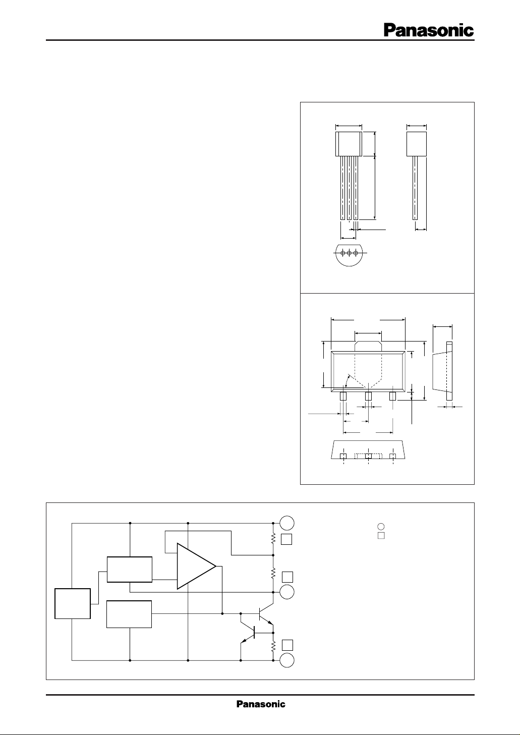
5.0±0.2
2.54
321
(Bottom View)
TO-92 Package (SSIP003-P-0000)
AN79L00M Series
2.6
45˚
0.45
4.6max.
1.8max.
2.3±0.2
2.6max.
Unit:mmAN79L00 Series
1 : Output
2 : Common
3 : Input
Unit:mm
1.6max.
4.25max.
4.0±0.2
5.1±0.213.5±0.5
+0.2
– 0.1
■ Block Diagram
Voltage
Reference
Starter
Thermal
Protection
+
Error Amp.
–
Current
Limiter
0.48max.
123
3-pin Mini Power type Plastic Package (TO-243) (SSIP003-P-0000D)
Common
2
R
1
1
R
2
3
Output
1
Q
1
Pass Tr.
2
R
SC
Input
3
Pin Number in are for AN79L00 Series
Pin Number in are for AN79L00M Series
0.53max.
1.5
3.0
0.8min.
0.44max.
1 : Common
2 : Input
3 : Output
Page 2
■ Absolute Maximum Ratings (Ta=25˚C)
Parameter Symbol Rating Unit
1
*
Input voltage
Power dissipation
Operating ambient temperature
Storage temperature
*
1 AN79L04/M, AN79L05/M, AN79L06/M, AN79L07/M, AN79L08/M, AN79L09/M, AN79L10/M, AN79L12/M,
AN79L00 Series
AN79L00M Series
V
I
P
D
T
opr
T
stg
–35
2
*
–40
3
*
650
–20 to +80
–55 to +150
–55 to +125
AN79L15/M, AN79L18/M
*
2 AN79L20/M, AN79L24/M
*
3 Follow the derating curve. When Tj exceeds 150˚C, the internal circuit cuts off the output.
Mounting onto the PCB (20 × 20 × 1.7 mm glass epoxy copper foil 1 cm2 or more), for AN79L00M Series.
■ Electrical Characteristics (Ta=25˚C)
AN79L04/AN79L04M (–4V Type)
·
Parameter Symbol Condition min typ max
Output voltage
Output voltage tolerance
Line regulation
Load regulation
Bias current
Input bias current fluctuation
Load bias current fluctuation
Output noise voltage
Ripple rejection ratio
Minimum input/output voltage difference
Output short circuit current
Output voltage temperature coefficient
Note 1) The specified condition T
=25˚C means that the test should be carried out with the test time so short (within 10ms) that the
j
V
V
REG
REG
I
Bias
∆I
bias (IN)
∆I
bias (L)
V
RR
V
DIF (min.)
I
O (Short)
∆VO/Ta
drift in characteristic value due to the rise in chip junction temperature can be ignored.
Note 2) When not specified, VI=–9V, IO=40mA, CI=2µF, CO=1µF, Tj=0 to 125˚C (AN79L04)
and Tj=0 to 100˚C (AN79L04)
T
=25˚C
O
O
j
VI=–7 to –19V, IO=1 to 70mA
=–6 to –20V, Tj=25˚C
V
I
IN
=–7 to –17V, Tj=25˚C
V
I
=1 to 100mA, Tj=25˚C
I
O
L
=1 to 40mA, Tj=25˚C
I
O
T
=25˚C
j
=–7 to –19V, Tj=25˚C
V
I
IO=1 to 40mA, Tj=25˚C
f=10Hz to 100kHz, Ta=25˚C
no
VI=–7 to –17V, f=120Hz, Ta
=25˚C
T
j
=–35V, Tj=25˚C
V
I
IO=5mA
=25˚C
–3.84
–3.8
4.5
38
55
– 0.4
mW
–4.16 V–4
–4.2
80 mV
40
60
30
5
0.5
0.1
V
V
˚C
˚C
Unit
V
mV
mV10
mV
mA3
mA
mA
µV
dB
V0.8
mA200
mV/˚C
Page 3
■ Electrical Characteristics (Ta=25˚C)
AN79L05/AN79L05M (–5V Type)
·
Parameter Symbol Condition min typ max
Output voltage
Output voltage tolerance
Line regulation
Load regulation
Bias current
Input bias current fluctuation
Load bias current fluctuation
Output noise voltage
Ripple rejection ratio
Minimum input/output voltage difference
Output short circuit current
Output voltage temperature coefficient
Note 1) The specified condition T
=25˚C means that the test should be carried out with the test time so short (within 10ms) that the
j
V
V
REG
REG
I
Bias
∆I
bias (IN)
∆I
bias (L)
V
RR
V
DIF (min.)
I
O (Short)
∆VO/Ta
drift in characteristic value due to the rise in chip junction temperature can be ignored.
Note 2) When not specified, VI=–9V, IO=40mA, CI=2µF, CO=1µF, Tj=0 to 125˚C (AN79L04)
and Tj=0 to 100˚C (AN79L04)
AN79L06/AN79L06M (–6V Type)
·
Parameter Symbol Condition min typ max
Output voltage
Output voltage tolerance
Line regulation
Load regulation
Bias current
Input bias current fluctuation
Load bias current fluctuation
Output noise voltage
Ripple rejection ratio
Minimum input/output voltage difference
Output short circuit current
Output voltage temoerature coefficient
Note 1) The specified condition T
=25˚C means that the test should be carried out with the test time so short (within 10ms) that the
j
V
V
REG
REG
I
Bias
∆I
bias (IN)
∆I
bias (L)
V
RR
V
DIF (min.)
I
O (Short)
∆VO/Ta
drift in characteristic value due to the rise in chip junction temperature can be ignored.
Note 2) When not specified, VI=–9V, IO=40mA, CI=2µF, CO=1µF, Tj=0 to 125˚C (AN79L04)
and Tj=0 to 100˚C (AN79L04)
T
=25˚C
O
O
j
VI=–8 to –20V, IO=1 to 70mA
VI=–7 to –21V, Tj=25˚C
IN
=–8 to –18V, Tj=25˚C
V
I
I
=1 to 100mA, Tj=25˚C
O
L
IO=1 to 40mA, Tj=25˚C
Tj=25˚C
V
=–8 to –20V, Tj=25˚C
I
IO=1 to 40mA, Tj=25˚C
f=10Hz to 100kHz, Ta=25˚C
no
VI=–8 to –18V, f=120Hz, Ta
Tj=25˚C
VI=–35V, Tj=25˚C
IO=5mA
T
=25˚C
O
O
j
VI=–79to –21V, IO=1 to 70mA
VI=–8 to –22V, Tj=25˚C
IN
=–9 to –19V, Tj=25˚C
V
I
I
=1 to 100mA, Tj=25˚C
O
L
IO=1 to 40mA, Tj=25˚C
Tj=25˚C
V
=–9 to –21V, Tj=25˚C
I
IO=1 to 40mA, Tj=25˚C
f=10Hz to 100kHz, Ta=25˚C
no
VI=–9 to –19V, f=120Hz, Ta
Tj=25˚C
VI=–35V, Tj=25˚C
IO=5mA
=25˚C
=25˚C
–4.8
–4.75
–5.76
–5.7
Unit
–5.2 V–5
–5.25
V
100 mV
mV
50
mV11
60
mV
30
5
mA3
5
mA
0.5
mA
0.1
40
55
µV
dB
V0.8
mA200
– 0.4
mV/˚C
Unit
–6.24 V–6
–6.3
V
120 mV
mV
60
mV12
60
mV
0.5
0.1
30
mA3
5
mA
mA
µV
dB
5.5
44
55
V0.8
mA200
–0.4
mV/˚C
Page 4

■ Electrical Characteristics (Ta=25˚C)
AN79L07/AN79L07M (–7V Type)
·
Parameter Symbol Condition min typ max
Output voltage
Output voltage tolerance
Line regulation
Load regulation
Bias current
Input bias current fluctuation
Load bias current fluctuation
Output noise voltage
Ripple rejection ratio
Minimum input/output voltage difference
Output short circuit current
Output voltage temperature coefficient
Note 1) The specified condition T
=25˚C means that the test should be carried out with the test time so short (within 10ms) that the
j
V
V
REG
REG
I
Bias
∆I
bias (IN)
∆I
bias (L)
V
RR
V
DIF (min.)
I
O (Short)
∆VO/Ta
drift in characteristic value due to the rise in chip junction temperature can be ignored.
Note 2) When not specified, VI=–9V, IO=40mA, CI=2µF, CO=1µF, Tj=0 to 125˚C (AN79L04)
and Tj=0 to 100˚C (AN79L04)
AN79L08/AN79L08M (–8V Type)
·
Parameter Symbol Condition min typ max
Output voltage
Output voltage tolerance
Line regulation
Load regulation
Bias current
Input bias current fluctuation
Load bias current fluctuation
Output noise voltage
Ripple rejection ratio
Minimum input/output voltage difference
Output short circuit current
Output voltage temperature coefficient
Note 1) The specified condition T
=25˚C means that the test should be carried out with the test time so short (within 10ms) that the
j
V
V
REG
REG
I
Bias
∆I
bias (IN)
∆I
bias (L)
V
RR
V
DIF (min.)
I
O (Short)
∆VO/Ta
drift in characteristic value due to the rise in chip junction temperature can be ignored.
Note 2) When not specified, VI=–9V, IO=40mA, CI=2µF, CO=1µF, Tj=0 to 125˚C (AN79L04)
and Tj=0 to 100˚C (AN79L04)
T
=25˚C
O
O
j
VI=–10 to –22V, IO=1 to 70mA
VI=–9 to –23V, Tj=25˚C
IN
=–10 to –20V, Tj=25˚C
V
I
I
=1 to 100mA, Tj=25˚C
O
L
IO=1 to 40mA, Tj=25˚C
Tj=25˚C
V
=–10 to –22V, Tj=25˚C
I
IO=1 to 40mA, Tj=25˚C
f=10Hz to 100kHz, Ta=25˚C
no
VI=–10 to –20V, f=120Hz, Ta
Tj=25˚C
VI=–35V, Tj=25˚C
IO=5mA
T
=25˚C
O
O
j
VI=–11 to –23V, IO=1 to 70mA
VI=–10 to –24V, Tj=25˚C
IN
=–11 to –21V, Tj=25˚C
V
I
I
=1 to 100mA, Tj=25˚C
O
L
IO=1 to 40mA, Tj=25˚C
Tj=25˚C
V
=–11 to –23V, Tj=25˚C
I
IO=1 to 40mA, Tj=25˚C
f=10Hz to 100kHz, Ta=25˚C
no
VI=–11 to –21V, f=120Hz, Ta
Tj=25˚C
VI=–35V, Tj=25˚C
IO=5mA
=25˚C
=25˚C
–6.72
–6.65
–7.68
–7.6
Unit
–7.28 V–7
–7.35
V
140 mV
mV
70
mV13
70
mV
40
6
mA3
5
mA
0.5
mA
0.1
48
54
µV
dB
V0.8
mA200
– 0.5
mV/˚C
Unit
–8.32 V–8
–8.4
V
160 mV
mV
80
mV15
80
mV
40
7
mA3
5
mA
0.5
mA
0.1
52
54
µV
dB
V0.8
mA200
– 0.6
mV/˚C
Page 5

■ Electrical Characteristics (Ta=25˚C)
AN79L09/AN79L09M (–9V Type)
·
Prameter Symbol Condition min typ max
Output voltage
Output voltage tolerance
Line regulation
Load regulation
Bias current
Input bias current fluctuation
Load bias current fluctuation
Output noise voltage
Ripple rejection ratio
Minimum input/output voltage difference
Output short circuit current
Output voltage temperature coefficient
Note 1) The specified condition T
=25˚C means that the test should be carried out with the test time so short (within 10ms) that the
j
V
V
REG
REG
I
Bias
∆I
bias (IN)
∆I
bias (L)
V
RR
V
DIF (min.)
I
O (Short)
∆VO/Ta
drift in characteristic value due to the rise in chip junction temperature can be ignored.
Note 2) When not specified, VI=–9V, IO=40mA, CI=2µF and CO=1µF, Tj=0 to 125˚C (AN79L04)
and Tj=0 to 100˚C (AN79L04)
AN79L10/AN79L10M (–10V Type)
·
Patameter Symbol Condition min typ max
Output voltage
Output voltage tolerance
Line regulation
Load regulation
Bias current
Input bias current fluctuation
Load bias current fluctuation
Output noise voltage
Ripple rejection
Minimum input/output voltage difference
Ouptput short circuit current
Output voltage temperature coefficient
Note 1) The specified condition T
=25˚C means that the test should be carried out with the test time so short (within 10ms) that the
j
V
V
REG
REG
I
Bias
∆I
bias (IN)
∆I
bias (L)
V
RR
V
DIF (min.)
I
O (Short)
∆VO/Ta
drift in characteristic value due to the rise in chip junction temperature can be ignored.
Note 2) When not specified, V
and T
=0 to 100˚C (AN79L04)
j
=–9V, IO=40mA, CI=2µF, CO=1µF, Tj=0 to 125˚C (AN79L04)
I
T
=25˚C
O
O
j
VI=–12 to –24V, IO=1 to 70mA
VI=–11 to –25V, Tj=25˚C
IN
=–12 to –22V, Tj=25˚C
V
I
I
=1 to 100mA, Tj=25˚C
O
L
IO=1 to 40mA, Tj=25˚C
Tj=25˚C
V
=–12 to –24V, Tj=25˚C
I
IO=1 to 40mA, Tj=25˚C
f=10Hz to 100kHz, Ta=25˚C
no
VI=–12 to –22V, f=120Hz, Ta
Tj=25˚C
VI=–35V, Tj=25˚C
IO=5mA
T
=25˚C
O
O
no
j
VI=–13 to –25V, IO=1 to 70mA
VI=–12 to –26V, Tj=25˚C
IN
=–13 to –23V, Tj=25˚C
V
I
I
=1 to 100mA, Tj=25˚C
O
L
=1 to 40mA, Tj=25˚C
I
O
T
=25˚C
j
V
=–13 to –25V, Tj=25˚C
I
=1 to 40mA, Tj=25˚C
I
O
f=10Hz to 100kHz, Ta=25˚C
VI=–13 to –23V, f=120Hz, Ta
=25˚C
T
j
VI=–35V, Tj=25˚C
=5mA
I
O
=25˚C
=25˚C
–8.64
–8.55
–9.6
–9.5
53
53
– 0.6
8
58
9
65
–9.36 V–9
–9.45
160 mV
80
90
50
5
0.5
0.1
mV/˚C
–10.4 V–10
–10.5
160 mV
80
100
50
5
0.5
0.1
mV/˚C– 0.7
Unit
V
mV
mV16
mV
mA3
mA
mA
µV
dB
V0.8
mA200
Unit
V
mV
mV17
mV
mA3
mA
mA
µV
dB
V0.8
mA200
Page 6

■ Electrical Characteristics (Ta=25˚C)
AN79L12/AN79L12M (–12V Type)
·
Parameter Symbol Condition min typ max
Output voltage
Output voltage tolerance
Line regulation
Load regulation
Bias current
Input bias current fluctuation
Load bias current fluctuation
Output noise voltage
Ripple rejection ratio
Minimum input/output voltage difference
Output short circuit current
Output voltage temperature
Note 1) The specified condition T
=25˚C means that the test should be carried out with the test time so short (within 10ms) that the
j
V
V
REG
REG
I
Bias
∆I
bias (IN)
∆I
bias (L)
V
RR
V
DIF (min.)
I
O (Short)
∆VO/Ta
drift in characteristic value due to the rise in chip junction temperature can be ignored.
Note 2) When not specified, VI=–9V, IO=40mA, CI=2µF, CO=1µF, Tj=0 to 125˚C (AN79L04)
and Tj=0 to 100˚C (AN79L04)
AN79L15T/AN79L15M (–15V Type)
·
Parameter Symbol Condition min typ max
Ouyput voltage
Output voltage tolerance
Line regulation
Load regulation
Bias current
Input bias current fluctuation
Load bias current fluctuation
Output noise voltage
Ripple rejection ratio
Minimum input/output voltage difference
Output short circuit current
Output voltage temperature coefficient
Note 1) The specified condition T
=25˚C means that the test should be carried out with the test time so short (within 10ms) that the
j
V
V
REG
REG
I
Bias
∆I
bias (IN)
∆I
bias (L)
V
RR
V
DIF (min.)
I
O (Short)
∆VO/Ta
drift in characteristic value due to the rise in chip junction temperature can be ignored.
Note 2) When not specified, VI=–9V, IO=40mA, CI=2µF, CO=1µF, Tj=0 to 125˚C (AN79L04)
and Tj=0 to 100˚C (AN79L04)
T
=25˚C
O
O
j
VI=–15 to –27V, IO=1 to 70mA
VI=–14.5 to –30V, Tj=25˚C
IN
=–15 to –25V, Tj=25˚C
V
I
I
=1 to 100mA, Tj=25˚C
O
L
IO=1 to 40mA, Tj=25˚C
Tj=25˚C
V
=–15 to –27V, Tj=25˚C
I
IO=1 to 40mA, Tj=25˚C
f=10Hz to 100kHz, Ta=25˚C
no
VI=–15 to –25V, f=120Hz, Ta
Tj=25˚C
VI=–35V, Tj=25˚C
IO=5mA
T
=25˚C
O
O
j
VI=–18 to –28V, IO=1 to 70mA
VI=–17.5 to –33V, Tj=25˚C
IN
=–18 to –28V, Tj=25˚C
V
I
I
=1 to 100mA, Tj=25˚C
O
L
IO=1 to 40mA, Tj=25˚C
Tj=25˚C
V
=–18 to –30V, Tj=25˚C
I
IO=1 to 40mA, Tj=25˚C
f=10Hz to 100kHz, Ta=25˚C
no
VI=–18 to –28V, f=120Hz, Ta
Tj=25˚C
VI=–35V, Tj=25˚C
IO=5mA
=25˚C
=25˚C
–11.5
–11.4
–14.4
–14.25
Unit
–12.5 V–12
–12.6
V
200 mV
0.5
0.1
mV
mV20
mV
50
mA3
5
mA
mA
µV
dB
100
100
10
75
52
V0.8
mA200
– 0.8
mV/˚C
Unit
–15.6 V–15
–15.75
V
200 mV
0.5
0.1
mV
mV25
mV
60
mA3
5
mA
mA
µV
dB
100
130
12
90
51
V0.8
mA200
– 0.9
mV/˚C
Page 7

■ Electrical Characteristics (Ta=25˚C)
AN79L18T/AN79L18M (–18V Type)
·
Parameter Symbol Condition min typ max
Output voltage
Output voltage tolerance
Line regulation
Load regulation
Bias current
Input bias current fluctuation
Load bias current fluctuation
Output noise voltage
Ripple rejection ratio
Minimum input/output voltage difference
Output short circuit current
Output voltage temperature coefficient
Note 1) The specified condition T
=25˚C means that the test should be carried out with the test time so short (within 10ms) that the
j
V
V
REG
REG
I
Bias
∆I
bias (IN)
∆I
bias (L)
V
RR
V
DIF (min.)
I
O (Short)
∆VO/Ta
drift in characteristic value due to the rise in chip junction temperature can be ignored.
Note 2) When not specified, VI=–9V, IO=40mA, CI=2µF, CO=1µF, Tj=0 to 125˚C (AN79L04)
and Tj=0 to 100˚C (AN79L04)
AN79L20T/AN79L20M (–20V Type)
·
Parameter Symbol Condition min typ max
Output voltage
Output voltage tolerance
Line regulation
Load regulation
Bias current
Input bias current fluctuation
Load bias current fluctuation
Output noise voltage
Ripple rejection ratio
Minimum input/output voltage difference
Output short circuit current
Output voltage temperature coefficient
Note 1) The specified condition T
=25˚C means that the test should be carried out with the test time so short (within 10ms) that the
j
V
V
REG
REG
I
Bias
∆I
bias (IN)
∆I
bias (L)
V
RR
V
DIF (min.)
I
O (Short)
∆VO/Ta
no
drift in characteristic value due to the rise in chip junction temperature can be ignored.
Note 2) When not specified, VI=–9V, IO=40mA, CI=2µF, CO=1µF, Tj=0 to 125˚C (AN79L04)
and Tj=0 to 100˚C (AN79L04)
T
=25˚C
O
O
j
VI=–21 to –33V, IO=1 to 70mA
VI=–21 to –33V, Tj=25˚C
IN
=–21 to –32V, Tj=25˚C
V
I
I
=1 to 100mA, Tj=25˚C
O
L
IO=1 to 40mA, Tj=25˚C
Tj=25˚C
V
=–21 to –33V, Tj=25˚C
I
IO=1 to 40mA, Tj=25˚C
f=10Hz to 100kHz, Ta=25˚C
no
VI=–22 to –32V, f=120Hz, Ta
Tj=25˚C
VI=–35V, Tj=25˚C
IO=5mA
T
=25˚C
O
O
j
VI=–23 to –35V, IO=1 to 70mA
VI=–23 to –35V, Tj=25˚C
IN
=–24 to –34V, Tj=25˚C
V
I
I
=1 to 100mA, Tj=25˚C
O
L
IO=1 to 40mA, Tj=25˚C
Tj=25˚C
V
=–23 to –35V, Tj=25˚C
I
IO=1 to 40mA, Tj=25˚C
f=10Hz to 100kHz, Ta=25˚C
VI=–24 to –34V, f=120Hz, Ta
Tj=25˚C
VI=–35V, Tj=25˚C
IO=5mA
=25˚C
=25˚C
–17.3
–17.1
–19.2
–19
Unit
–18.7 V–18
–18.9
V
200 mV
0.5
0.1
mV
mV30
mV
80
mA3
5
mA
mA
µV
dB
100
160
15
110
50
V0.8
mA200
–1
mV/˚C
Unit
–20.8 V–20
–21
V
200 mV
90
0.5
0.1
mV
mV35
mV
mA3
5
mA
mA
µV
dB
100
180
17
135
49
V0.8
mA200
–1
mV/˚C
Page 8

■ Electrical Characteristics (Ta=25˚C)
AN79L24/AN79L24M (–24V Type)
·
Parameter Symbol Condition min typ max
Output voltage
Output voltage tolerance
Line regulation
Load regulation
Bias current
Input bias current fluctuation
Load bias current fluctuation
Output noise voltage
Ripple rejection ratio
Minimum input/output voltage difference
Output short circuit current
Output voltage temperature coefficient
Note 1) The specified condition T
=25˚C means that the test should be carried out with the test time so short (within 10ms) that the
j
V
V
REG
REG
I
Bias
∆I
bias (IN)
∆I
bias (L)
V
RR
V
DIF (min.)
I
O (Short)
∆VO/Ta
T
=25˚C
O
O
j
VI=–27 to –38V, IO=1 to 70mA
VI=–27 to –38V, Tj=25˚C
IN
=–27 to –37V, Tj=25˚C
V
I
I
=1 to 100mA, Tj=25˚C
O
L
IO=1 to 40mA, Tj=25˚C
Tj=25˚C
V
=–27 to –38V, Tj=25˚C
I
IO=1 to 40mA, Tj=25˚C
f=10Hz to 100kHz, Ta=25˚C
no
VI=–28 to –38V, f=120Hz, Ta
Tj=25˚C
VI=–35V, Tj=25˚C
IO=5mA
=25˚C
–23
–22.8
49
drift in characteristic value due to the rise in chip junction temperature can be ignored.
Note 2) When not specified, VI=–9V, IO=40mA, CI=2µF, CO=1µF, Tj=0 to 125˚C (AN79L04)
and Tj=0 to 100˚C (AN79L04)
■ Basic Regulator Circuit ■ A pplication Circuit
170
20
–1
–25 V–24
–25.2
200 mV
100
200
100
5
0.5
0.1
mV/˚C
Unit
V
mV
mV40
mV
mA3
mA
mA
µV
dB
V0.8
mA200
–V
I
Input
3
1
Output
–V
O
AN79L00
–
C
I
2
+
Common
–
C
O
+
CI is connected when the input line is long. 2µF
improves the transient Response. 1µF
C
O
–V
Input Output
I
3
1
–V
O
AN79L00
R
2µF
–
+
Common
2
|VO|= VO´ 1 + + IQR
I
Q
R
R
2
–
VO´
1
2
1µF
+
R
1
1
Page 9

■ Characteristic Curve
PD –Ta (AN79L00 Series)
1.0
0.8
(W)
D
0.6
0.4
Power Dissipation P
0.2
0
0 20 40 60 80 100 120 140 160
Ambient Temperature Ta (˚C)
1.4
(V)
DIF (min.)
1.2
1.0
0.8
0.6
V
I
DIF (min.)
IO=100mA
I
O
=20mA
I
O
=10mA
O
=1mA
– T
j
AN79L05
PD –Ta (AN79L00 M Series)
1.0
Mounting onto the PCB,
20 × 20 × 1.7mm
0.8
(W)
D
0.6
0.4
Power Dissipation P
0.2
0
0 20 40 60 80 100 120 140 160
Glass Epoxy Substrate,
Copper Foil 1cm
2
Ambient Temperature Ta (˚C)
Input Transient Response
AN79L05
10
0
–10
or More
–5.12
–5.08
–5.04
(V)
O
–5.00
–4.96
–4.92
Output Voltage V
–4.88
–4.84
–4.80
–25 0 25 50 75 100 125
20
(V)
I
15
10
Input Voltage V
5
1
0
–1
VO – T
j
AN79L05
=–10V
V
I
=1mA
I
O
Junction Temperature T
j
(˚C)
Load Transient Response
AN79L05
200
(mA)
O
100
0
Load Current I
0.4
–50 0 50 100 150
Minimum Input/Output Voltage Difference V
Junction Temperature Tj (˚C)
RR– f
120
100
80
60
40
20
Ripple Rejection Ratio RR (dB)
0
10 100
Frequency f (Hz)
AN79L05
I
=5mA
O
1k 10k 100k
–20
0246810
Output Voltage Fluctuation (mV)
Time t (µs)
–2
Output Voltage Fluctuation (V)
0 1020304050
Time t (µs)
 Loading...