

Page 1
AN7800R/AN78M00R Series
Positive Output Voltage Regulators with
Reset pin (1A/500mA Type)
■ Overview
The AN7800R and the AN78M00R series are the fix ed
positive output voltage regulators with reset pin. Stabilized fixed output voltage is obtained from unstable DC
input voltage without using any external components.
Three types of output voltage, 5V, 9V and 12V, are available for the AN7800R series, and four types, 5V, 8V, 9V
and 12V, are available for the AN78M00R series. They
can be used in power circuits with current capacitance
1A/500mA. ON/OFF of output voltage can be controlled
by the reset pin.
3–1.0
12.5max.
1.8
9.6
+ 0.5
– 0.1
ø 3.1
2.3 1.5 1.32.32.3
Unit:mm
4.0
2.0
9.0min.
0.7±0.2 0.5±0.1
■ Features
• No external components
• Maximum output current :1A (AN7800R)
500mA (AN78M00R)
• Output voltage :5V, 9V, 12V (AN7800R)
:8V (AN78M08R)
• Short-circuit current limiting built-in
• Thermal overload protection built-in
• Output transistor safe area compensation
• ON/OFF of output voltage can be controlled by reset
pin.
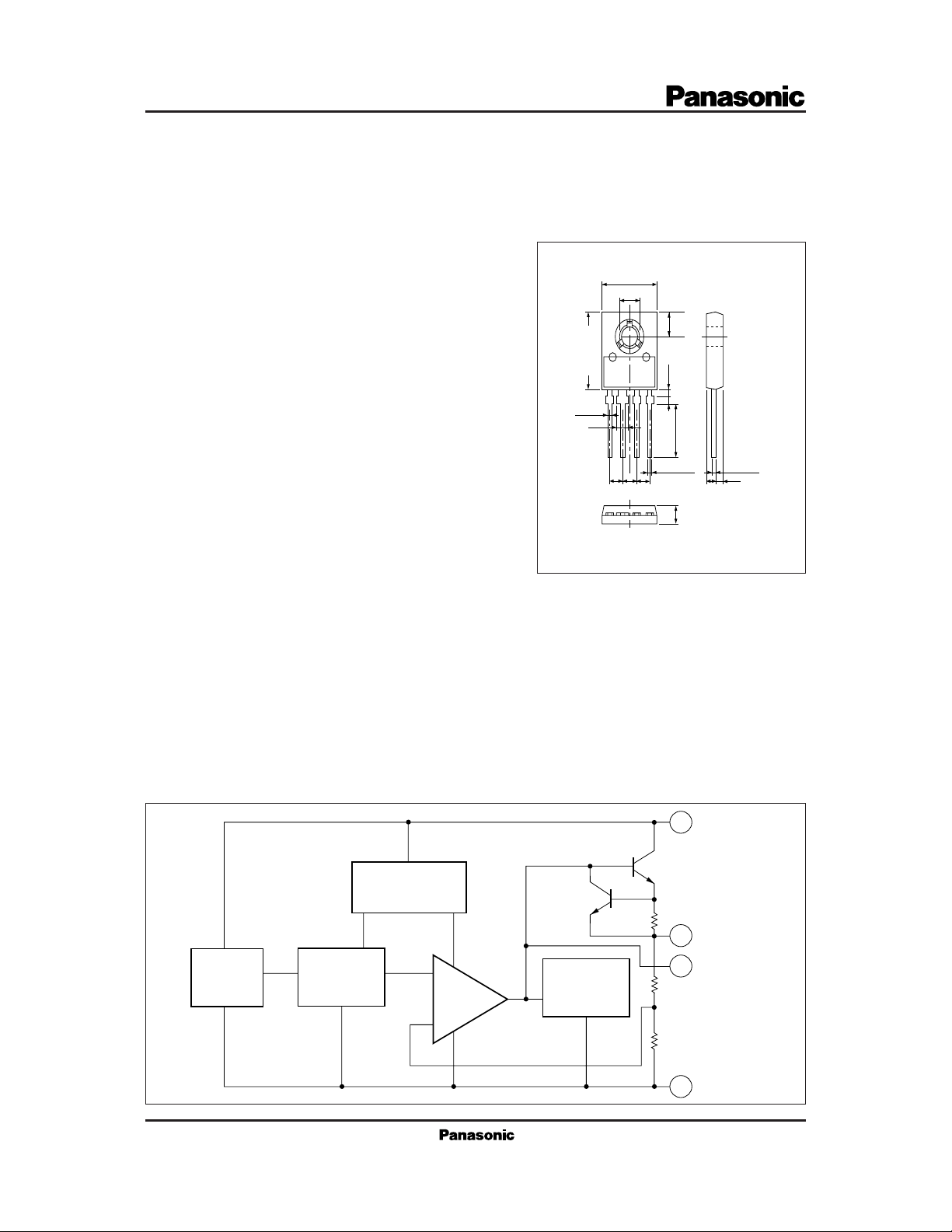
■ Block Diagram
Current
Source
Starter
Voltage
Reference
+
Error Amp.
–
3.3max.
4-pin SIL Plastic Package with Fin (SSIP004-P-0000)
Input
1
Pass Tr
Q
1
Current
Limiter
Thermal
Protection
R
SC
Output
3
Reset
4
R
2
R
1
2
Common
Page 2
■ Absolute Maximum Ratings (Ta=25˚C)
Parameter Symbol Rating Unit
Input voltage
Power dissipation
Operating ambient temperature
Storage temperature
*
1 Follow the derating curve. When Tj exceeds 150˚C, the internal circuit cuts off the output.
V
I
P
D
T
opr
T
stg
35
1
*
10
–20 to + 80
–55 to + 150
V
W
˚C
˚C
■ Electrical Characteristics (Ta=25˚C)
AN7800R Series
AN7805R (1A, 5V Type)
·
Parameter Symbol Condition min typ max Unit
Output voltage
Output voltage tolerance
Line regulation
Load regulation
Bias current
Input bias current fluctuation
Load bias current fluctuation
Output noise voltage
Ripple rejection ratio
Minimum input/output voltage difference
Output impedance
Output short circuit current
Peak output current
Output voltage temperature coefficient
Output voltage at reset
Reset input current
V
V
REG
REG
I
bias
∆I
bias (IN)
∆I
bias (L)
V
RR
V
DIF (min.)
I
O (Short)
I
O (Peak)
∆VO/Ta
O (Reset)
I (Reset)
O
O
no
O
Note 1) The specified condition Tj=25˚C means that the test should be carried out with the test time so short (within 10ms) that the
drift in characteristic value due to the rise in chip junction temperature can be ignored.
Note 2) When not specified, VI=10V, IO=100mA, CI=0.33µF, CO=0.1µF, Tj=0 to 125˚C
=25˚C
T
j
=8 to 20V, IO=5mA to 1A,
V
I
=0 to 125˚C, P
T
j
=7.5 to 25V, Tj=25˚C
V
I
IN
=8 to 12V, Tj=25˚C
V
I
=5mA to 1.5A, Tj=25˚C
I
O
L
=250 to 750mA, Tj=25˚C
I
O
=25˚C
T
j
=7.5 to 25V, Tj=25˚C
V
I
=5mA to 1A, Tj=25˚C
I
O
f=10Hz to 100kHz
VI=8 to 18V, IO=100mA, f=120Hz
=1A, Tj=25˚C
I
O
f=1kHz
=35V, Tj=25˚C
V
I
Tj=25˚C
IO=5mA, Tj=0 to 125˚C
Tj=25˚C, I
I (Reset)
Tj=25˚C
<
D
=
=1mA
15W
4.8
4.75
5.2 V5
5.25
100 mV3
1
100
5
1.3
0.5
mV
50
mV15
mV
50
mA3.9
8
mA
mA
62
mΩ17Z
mA700
mV/˚C– 0.3
mA1I
V
µV40
dB
V2
A2
V1V
Page 3

■ Electrical Characteristics (Ta=25˚C)
AN7809R (1A, 9V Type)
·
Parameter Symbol Condition min typ max Unit
Output voltage
Output voltage tolerance
Line regulation
Load regulation
Bias current
Input bias current fluctuation
Load bias current fluctuation
Output noise voltage
Ripple rejection ratio
Minimum input/output voltage difference
Output impedance
Output short circuit current
Peak output current
Output voltage temperature coefficient
Output voltage at reset
Reset input current
Note 1) The specified condition T
=25˚C means that the test should be carried out with the test time so short (within 10ms) that the
j
V
V
REG
REG
I
bias
∆I
bias (IN)
∆I
bias (L)
V
RR
V
DIF (min.)
I
O (Short)
I
O (Peak)
∆VO/Ta
V
O (Reset)
I
I (Reset)
O
O
no
O
drift in characteristic value due to the rise in chip junction temperature can be ignored.
Note 2) When not specified, VI=15V, IO=100mA, CI=0.33µF, CO=0.1µF, Tj=0 to 125˚C
=25˚C
T
j
=12 to 24V, IO=5mA to 1A,
V
I
=0 to 125˚C, P
T
j
=11.5 to 26V, Tj=25˚C
V
I
IN
=12 to 18V, Tj=25˚C
V
I
=5mA to 1.5A, Tj=25˚C
I
O
L
=250 to 750mA, Tj=25˚C
I
O
=25˚C
T
j
=11.5 to 26V, Tj=25˚C
V
I
=5mA to 1A, Tj=25˚C
I
O
D
f=10Hz to 100kHz
VI=12 to 22V, IO=100mA, f=120Hz
=1A, Tj=25˚C
I
O
f=1kHz
=26V, Tj=25˚C
V
I
Tj=25˚C
IO=5mA, Tj=0 to 125˚C
Tj=25˚C, I
I (Reset)
=1mA
Tj=25˚C
<
15W
=
8.65
8.55
9.35 V9
9.45
V
180 mV7
0.5
mV
90
mV12
mV
90
mA3.9
8
mA
1
mA
µV
dB
2
180
4
57
56
V2
16Z
mΩ
mA700
A2
– 0.5
mV/˚C
V1
mA1
AN7812R (1A, 12V Type)
·
Parameter Symbol Condition min typ max Unit
Output voltage
Output voltage tolerance
Line regulation
Load regulation
Bias current
Input bias current fluctuation
Load bias current fluctuation
Output noise voltage
Ripple rejection ratio
Minimum input/output voltage difference
Output impedance
Output short circuit current
Peak output current
Output voltage temperature coefficient
Output voltage at reset
Reset input current
Note 1) The specified condition T
=25˚C means that the test should be carried out with the test time so short (within 10ms) that the
j
V
V
REG
REG
I
bias
∆I
bias (IN)
∆I
bias (L)
V
RR
V
DIF (min.)
I
O (Short)
I
O (Peak)
∆VO/Ta
V
O (Reset)
I
I (Reset)
O
O
no
O
=25˚C
T
j
=15 to 27V, IO=5mA to 1A,
V
I
=0 to 125˚C, P
T
j
=14.5 to 30V, Tj=25˚C
V
I
IN
=16 to 22V, Tj=25˚C
V
I
=5mA to 1.5A, Tj=25˚C
I
O
L
=250 to 750mA, Tj=25˚C
I
O
=25˚C
T
j
=14.5 to 30V, Tj=25˚C
V
I
=5mA to 1A, Tj=25˚C
I
O
f=10Hz to 100kHz
VI=15 to 25V, IO=100mA, f=120Hz
=1A, Tj=25˚C
I
O
f=1kHz
=35V, Tj=25˚C
V
I
Tj=25˚C
IO=5mA, Tj=0 to 125˚C
Tj=25˚C, I
I (Reset)
=1mA
Tj=25˚C
D
<
=
15W
drift in characteristic value due to the rise in chip junction temperature can be ignored.
Note 2) When not specified, VI=19V, IO=100mA, CI=0.33µF, CO=0.1µF, Tj=0 to 125˚C
11.5
11.4
55
– 0.8
12.5 V12
12.6
V
240 mV10
0.5
mV
mV12
mV
mA4
8
mA
1
mA
µV
3
120
240
120
4
75
dB
V2
18Z
mΩ
mA700
A2
mV/˚C
V1
mA1
Page 4

■ Electrical Characteristics (Ta=25˚C)
AN78M00R Series
AN78M05R (500mA, 5V Type)
·
Parameter Symbol Condition min typ max Unit
=25˚C
Output voltage
Output voltage tolerance
Line regulation
Load regulation
Bias current
Input bias current fluctuation
Load bias current fluctuation
Output noise voltage
Ripple rejection ratio
Minimum input/output voltage difference
Output short circuit current
Peak output current
Output voltage temperature coefficient
Output voltage at reset
Reset input current
Note 1) The specified condition T
=25˚C means that the test should be carried out with the test time so short (within 10ms) that the
j
V
V
REG
REG
I
bias
∆I
bias (IN)
∆I
bias (L)
V
RR
V
DIF (min.)
I
O (Short)
I
O (Peak)
∆VO/Ta
V
O (Reset)
I
I (Reset)
drift in characteristic value due to the rise in chip junction temperature can be ignored.
Note 2) When not specified, VI=10V, IO=350mA, CI=0.33µF, CO=0.1µF, Tj=0 to 125˚C
T
O
O
no
j
=7.5 to 20V, IO=5 to 350mA,
V
I
T
=0 to 125˚C, P
j
=7.5 to 25V, Tj=25˚C
V
I
IN
=8 to 25V, Tj=25˚C
V
I
=5 to 500mA, Tj=25˚C
I
O
L
=5 to 200mA, Tj=25˚C
I
O
=25˚C
T
j
=8 to 25V, Tj=25˚C
V
I
=5 to 350mA, Tj=25˚C
I
O
f=10Hz to 100kHz
VI=8 to 18V, IO=100mA, f=120Hz
=500mA, Tj=25˚C
I
O
=35V, Tj=25˚C
V
I
Tj=25˚C
IO=5mA, Tj=0 to 125˚C
Tj=25˚C, I
T
=25˚C
j
I (Reset)
<
15W
D
=
=1mA
4.8
4.75
5.2 V5
5.25
V
100 mV3
0.8
0.5
mV
50
mV20
mV
50
mA4.6
6
mA
mA
1
100
10
µV40
1
dB
V
mA
mA
mV/˚C
V
62
2
300
700
– 0.5
mA1
AN78M08R (500mA, 8V Type)
·
Parameter Symbol Condition min typ max Unit
=25˚C
Output voltage
Output voltage tolerance
Line regulation
Load regulation
Bias current
Input bias current fluctuation
Load bias current fluctuation
Output noise voltage
Ripple rejection ratio
Minimum input/output voltage difference
Output short circuit current
Peak output current
Output voltage temperature coefficient
Output voltage at reset
Reset input current
Note 1) The specified condition T
=25˚C means that the test should be carried out with the test time so short (within 10ms) that the
j
V
V
REG
REG
I
bias
∆I
bias (IN)
∆I
bias (L)
V
RR
V
DIF (min.)
I
O (Short)
I
O (Peak)
∆VO/Ta
V
O (Reset)
I
I (Reset)
T
O
O
no
j
VI=10.5 to 23V, IO=5 to 350mA,
Tj=0 to 125˚C, P
IN
L
=11 to 25V, Tj=25˚C
V
I
=5 to 500mA, Tj=25˚C
I
O
=5 to 200mA, Tj=25˚C
I
O
=25˚C
T
j
=10.5 to 25V, Tj=25˚C
V
I
=5 to 350mA, Tj=25˚C
I
O
=10.5 to 25V, Tj=25˚C
V
I
f=10Hz to 100kHz
VI=11.5 to 21.5V, IO=100mA, f=120Hz
=500mA, Tj=25˚C
I
O
=35V, Tj=25˚C
V
I
Tj=25˚C
IO=5mA, Tj=0 to 125˚C
Tj=25˚C, I
I (Reset)
Tj=25˚C
<
D
=
=1mA
15W
drift in characteristic value due to the rise in chip junction temperature can be ignored.
Note 2) When not specified, VI=14V, IO=350mA, CI=0.33µF, CO=0.1µF, Tj=0 to 125˚C
7.7
7.6
8.3 V8
8.4
V
100 mV6
160
0.8
0.5
mV
50
mV25
mV
80
mA4.1
6
mA
mA
µV
dB
2
10
52
56
V2
mA300
A0.7
– 0.5
mV/˚C
V1
mA1
Page 5

■ Electrical Characteristics (Ta=25˚C)
AN78M09R (500mA, 9V Type)
·
Parameter Symbol Condition min typ max Unit
Output voltage
Output voltage tolerance
Line regulation
Load regulation
Bias current
Input bias current fluctuation
Load bias current fluctuation
Output noise voltage
Ripple rejection ratio
Minimum input/output voltage difference
Output short circuit current
Peak output current
Output voltage temperature coefficient
Output voltage at reset
Reset input current
Note 1) The specified condition T
=25˚C means that the test should be carried out with the test time so short (within 10ms) that the
j
drift in characteristic value due to the rise in chip junction temperature can be ignored.
Note 2) When not specified, VI=15V, IO=350mA, CI=0.33µF, CO=0.1µF, Tj=0 to 125˚C
V
V
REG
REG
I
bias
∆I
bias (IN)
∆I
bias (L)
V
RR
V
DIF (min.)
I
O (Short)
I
O (Peak)
∆VO/Ta
V
O (Reset)
I
I (Reset)
Tj=25˚C
O
VI=11.5 to 24V, IO=5 to 350mA,
O
Tj=0 to 125˚C, P
=11.5 to 25V, Tj=25˚C
V
I
IN
no
=12 to 25V, Tj=25˚C
V
I
=5 to 500mA, Tj=25˚C
I
O
L
=5 to 200mA, Tj=25˚C
I
O
=25˚C
T
j
=12 to 25V, Tj=25˚C
V
I
=5 to 350mA, Tj=25˚C
I
O
f=10Hz to 100kHz
VI=12 to 22V, IO=100mA, f=120Hz
=500mA, Tj=25˚C
I
O
=35V, Tj=25˚C
V
I
Tj=25˚C
IO=5mA, Tj=0 to 125˚C
Tj=25˚C, I
I (Reset)
Tj=25˚C
<
D
=
=1mA
15W
8.65
8.55
9.35 V9
9.45
V
100 mV7
6.0
0.8
0.5
mV
50
mV25
mV
90
mA4.1
mA
mA
µV
dB
2
180
10
60
56
V2
mA300
A0.7
– 0.5
mV/˚C
V1
mA1
AN78M12R (500mA, 12V Type)
·
Parameter Symbol Condition min typ max Unit
Output voltage
Output voltage tolerance
Line regulation
Load regulation
Bias current
Input bias current fluctuation
Load bias current fluctuation
Output noise voltage
Ripple rejection ratio
Minimum input/output voltage difference
Output short circuit current
Peak output current
Output voltage remperature coefficient
Output voltage at reset
Reset input current
Note 1) The specified condition T
=25˚C means that the test should be carried out with the test time so short (within 10ms) that the
j
V
V
REG
REG
I
bias
∆I
bias (IN)
∆I
bias (L)
V
RR
V
DIF (min.)
I
O (Short)
I
O (Peak)
∆VO/Ta
V
O (Reset)
I
I (Reset)
O
O
no
j
VI=14.5 to 27V, IO=5 to 350mA,
Tj=0 to 125˚C, P
IN
=16 to 30V, Tj=25˚C
V
I
=5 to 500mA, Tj=25˚C
I
O
L
=5 to 200mA, Tj=25˚C
I
O
=25˚C
T
j
=14.5 to 30V, Tj=25˚C
V
I
=5 to 350mA, Tj=25˚C
I
O
=14.5 to 30V, Tj=25˚C
V
I
f=10Hz to 100kHz
=25˚C
T
VI=15 to 25V, IO=100mA, f=120Hz
=500mA, Tj=25˚C
I
O
=35V, Tj=25˚C
V
I
Tj=25˚C, VI=35V
IO=5mA, Tj=0 to 125˚C
Tj=25˚C, I
I (Reset)
Tj=25˚C
<
D
=
=1mA
15W
drift in characteristic value due to the rise in chip junction temperature can be ignored.
Note 2) When not specified, VI=19V, IO=350mA, CI=0.33µF, CO=0.1µF, Tj=0 to 125˚C
11.5
11.4
12.5 V12
12.6
V
100 mV8
0.8
0.5
mV
50
mV25
mV
mA4.3
6
mA
mA
2
240
120
10
µV75
55
dB
V2
mA300
mA700
– 0.5
mV/˚C
V1
mA1
Page 6

■ Characteristic Curve
PD –Ta
16
14
12
(W)
D
Power Dissipation P
(1)
10
8
(2)
6
(3)
4
(4)
2
0
0 40 80 120 160
Ambient Temperature Ta (˚C)
(1) Infinite Heat Sink
(2) 5˚C/W Heat Sink
(3) 15˚C/W Heat Sink
(4) Without Heat Sink
(mV)
O (Reset)
Output Voltage at Reset V
■ Basic Regulator Circuit
Input Output
13
AN7800R
AN78M00R
C
I
2
*
7406etc.
4
Reset
1000
800
600
400
200
0
C
O
V
O (Reset)
VI=20V
VI=10V
VI=7V
0.1 1
Output Current IO (mA)
*
For TTL, an open collector type inverter, buffer, gate etc.
can be used.
Beware of the breakdown of TTL, as the reset pin bears voltage
higher than the output voltage VO by 1—2V.
– I
O
C
=0.33µF
I
=0.1µF
C
O
=25˚C
T
j
1.0
0.8
(mA)
0.6
I (Reset)
VI=30V
10 100 1000
0.4
Reset Current I
0.2
0
–40 0 40 80 120 160
Junction Temperature Tj (˚C)
C
is set when the input line is long.
I
CO improves the temperature response.
I
I (Reset)
– T
j
■ Applica tion Circuit
(1) Soft Start Circuit
Input
0.33µF
✼ Control of Output Voltage Rise Time
13
AN7800R
AN78M00R
10
1
0.1
Output Voltage Rise Time tr (s)
4
2
110
1kΩ
C
Capacity C (µF)
100
Output
0.1µF
(2) Several Output Reset Circuits
Input
0.33µF
Input
0.33µF
13
AN7800R
AN78M00R
13
AN7800R
AN78M00R
1kΩ
4
2
4
2
1kΩ R
Output
R
Q
SW
0.1µF
0.1µF
 Loading...