

Page 1
AN78L00/AN78L00M Series
3-pin Positive Output Voltage Regulator (100mA Type)
■ Overview
The AN78L00 ser ies is 3-pin fixed positive output type
monolithic voltage regulators.
A Stabilized fixed output voltage is obtained from an
unstable DC input voltage without using any external
parts. Eleven types of fixed output voltage are available
from 4V through 10V, 12V, 15V, 18V, 20V , and 24V. They
can be used widely as power circuits with a current
capacitance of up to 100mA.
■ Features
• No external components
• Output voltage:4V, 5V, 6V, 7V, 8V, 9V, 10V, 12V,
15V, 18V, 20V, 24V
• Internal short-circuit current limiting
• Internal thermal overload protection
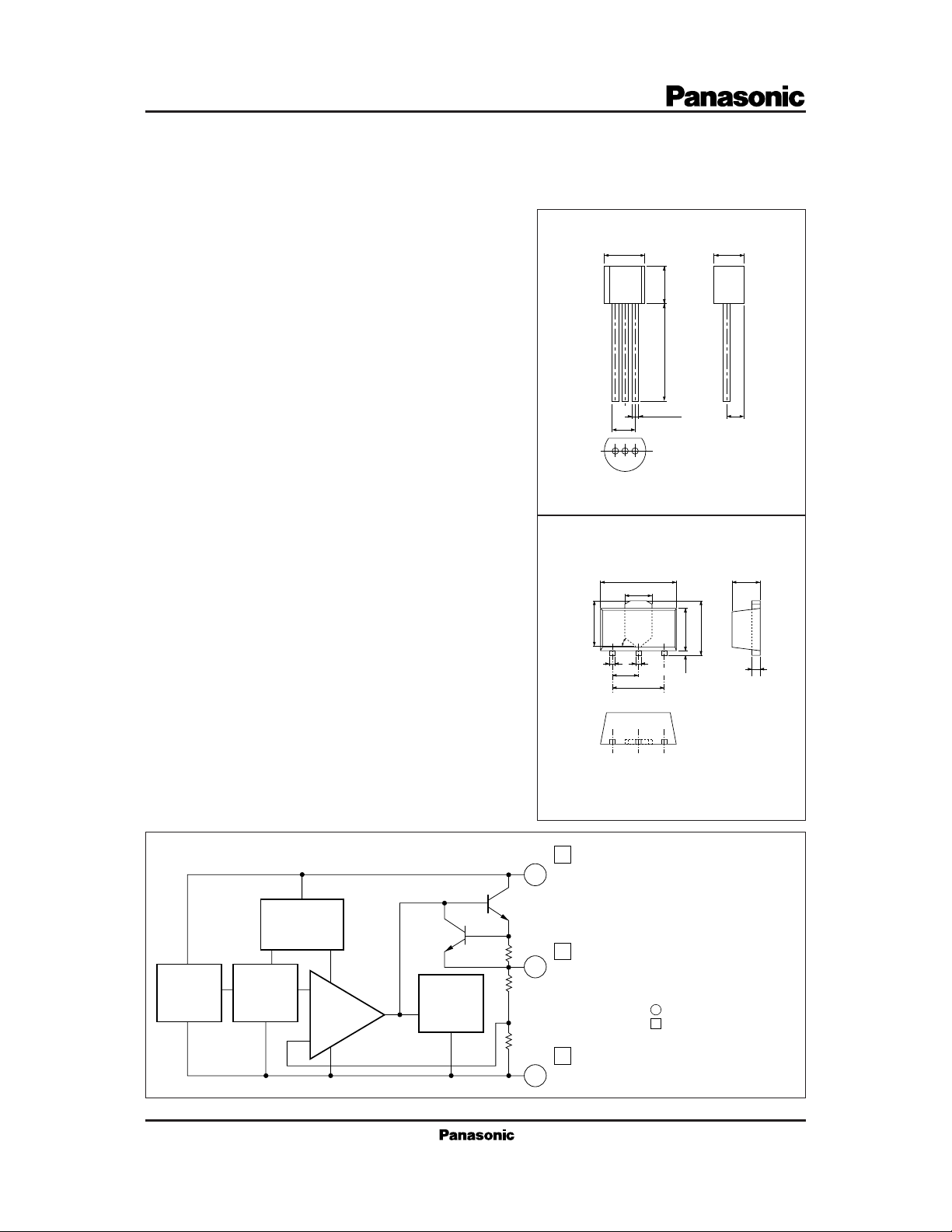
AN78L00 Series
AN78L00M Series Unit:mm
5.0±0.2
0.45
2.54
321
(Bottom View)
TO-92 Package (SSIP003-P-0000)
4.6max.
1.8max.
2.6
4.5
0.48max.
0.58max.
1.5
3.0
5.1±0.213.5±0.5
+0.2
– 0.1
2.6max.
0.8min.
1:Output
2:Common
3:Input
4.0±0.2
2.3±0.2
1.6max.
4.25max.
0.44max.
Unit:mm
1:Input
2:Output
3:Common
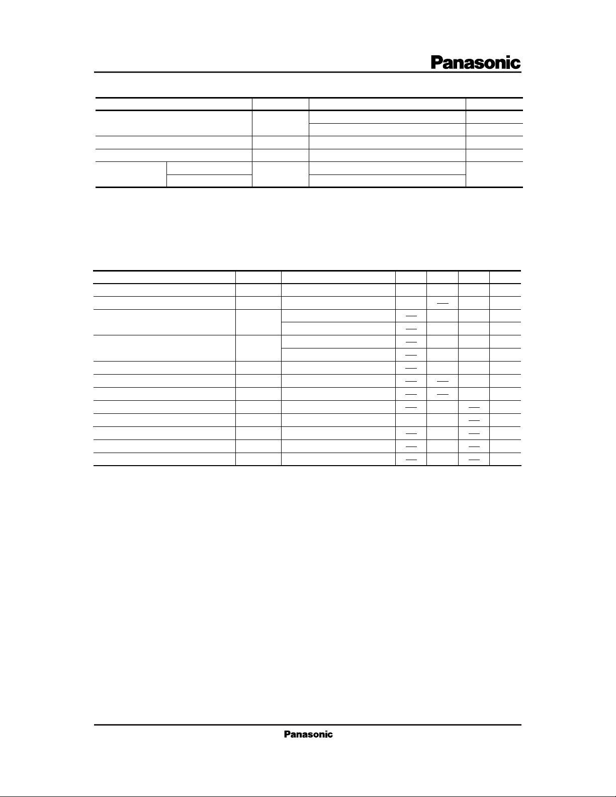
■ Block Diagram
Starter
Voltage
Reference
Current
Source
+
Error Amp.
–
Current
Limiter
Thermal
Protection
Pass Tr
Q
R
R
R
1
1
SC
2
2
1
3
123
3-pin SIL Mini Power Type Plastic Package (HSIP003-P-0000B)
3
Input
1
Output
Pin Number in are for AN78L00 Series
Pin Number in are for AN78L00M Series
2
Common
Page 2
■ Absolute Maximum Ratings (Ta=25˚C)
Parameter Symbol Rating Unit
1
*
Input voltage
Power dissipation
Operating ambient temperature
Storage temperature
*
1 AN78L04/M, AN78L05/M, AN78L06/M, AN78L07/M, AN78L08/M, AN78L09/M, AN78L10/M, AN78L12/M, AN78L15/M
*
2 AN78L18/M, AN78L20/M, AN78L24/M
*
3 Follow the derating curve. When Tj exceeds 150˚C, the internal circuit shuts off the output.
AN78L00 Series
AN78L00M Series
V
I
P
D
T
opr
T
stg
35
2
*
40
3
*
650
–30 to +80
–55 to +150
–55 to +125
Mounting onto the PCB (20 × 20 × 1.7mm glass epoxy copper foil 1cm2 or more), for AN78L00M Series.
■ Electrical Characteristics (Ta=25˚C)
AN78L04/AN78L04M (4V Type)
·
Parameter Symbol Condition min typ max
Output voltage
Output voltage tolerance
Line regulation
Load regulation
Bias current
Input bias current fluctuation
Load bias current fluctuation
Output noise voltage
Ripple rejection ratio
Minimum I/O voltage difference
Output short-circuit current
Output voltage temperature cofficient
Note 1) The specified condition T
=25˚C means that the test should be conducted with each test time reducedt (within 10ms) so that
j
V
V
REG
REG
I
bias
∆I
bias (IN)
∆I
bias (L)
V
RR
V
DIF (min.)
I
O (Short)
∆VO/Ta
O
O
no
the drift in characteristic value due to a temperature rise at chip junction can be innored.
Note 2) Unless otherwise specified, VI=9V, IO=40mA, CI=0.33µF, CO=0.1µF, Tj=0 to 125˚C (AN78L04) and Tj=0 to 100˚C
(AN78L04M).
=25˚C
T
j
=6.5 to 19V, Tj=25˚C
V
I
IN
=7 to 19V, Tj=25˚C
V
I
=1 to 100mA, Tj=25˚C
I
O
L
=1 to 40mA, Tj=25˚C
I
O
=25˚C
T
j
=7 to 19V, Tj=25˚C
V
I
=1 to 40mA, Tj=25˚C
I
O
f=10Hz to 100kHz
VI=7 to 17V, IO=40mA, f=120Hz
=25˚C
T
j
=25˚C, VI=35V
T
j
IO=5mA, Tj=0 to 125˚C
3.84
3.8
4.16 V4
4.2
145 mV50
40
95
55
4.5
30
3
1
0.1
40
48
58
– 0.6
V
V
mW
˚C
˚C
Unit
VVI=6.5 to 19V, IO=1 to 70mA
mV
mV10
mV
mA2
mA
mA
µV
dB
V1.7
mA140
mV/˚C
Page 3
■ Electrical Characteristics (Ta=25˚C)
AN78L05/AN78L05M (5V Type)
·
Parameter Symbol Condition min typ max
Output voltage
Output voltage tolerance
Line regulation
Load regulation
Bias current
Input bias current fluctuation
Load bias current fluctuation
Output noise voltage
Ripple rejection ratio
Minimum I/O voltage difference
Output short-circuit current
Output voltage temperature cofficient
Note 1) The specified condition T
=25˚C means that the test should be conducted with each test time reducedt (within 10ms) so that
j
V
V
REG
REG
I
bias
∆I
bias (IN)
∆I
bias (L)
V
RR
V
DIF (min.)
I
O (Short)
∆VO/Ta
O
O
no
the drift in characteristic value due to a temperature rise at chip junction can be innored.
Note 2) Unless otherwise specified, VI=10V, IO=40mA, CI=0.33µF, CO=0.1µF, Tj=0 to 125˚C (AN78L05) and Tj=0 to 100˚C
(AN78L05M).
AN78L06/AN78L06M (6V Type)
·
Parameter Symbol Condition min typ max
Output voltage
Output voltage tolerance
Line regulation
Load regulation
Bias current
Input bias current fluctuation
Load bias current fluctuation
Output noise voltage
Ripple rejection ratio
Minimum I/O voltage difference
Output short-circuit current
Output voltage temperature cofficient
Note 1) The specified condition T
=25˚C means that the test should be conducted with each test time reducedt (within 10ms) so that
j
V
V
REG
REG
I
bias
∆I
bias (IN)
∆I
bias (L)
V
RR
V
DIF (min.)
I
O (Short)
∆VO/Ta
O
O
no
the drift in characteristic value due to a temperature rise at chip junction can be innored.
Note 2) Unless otherwise specified, VI=11V, IO=40mA, CI=0.33µF, CO=0.1µF, Tj=0 to 125˚C (AN78L06) and Tj=0 to 100˚C
(AN78L06M).
=25˚C
T
j
=7.5 to 20V, Tj=25˚C
V
I
IN
=8 to 20V, Tj=25˚C
V
I
=1 to 100mA, Tj=25˚C
I
O
L
=1 to 40mA, Tj=25˚C
I
O
=25˚C
T
j
=8 to 20V, Tj=25˚C
V
I
=1 to 40mA, Tj=25˚C
I
O
f=10Hz to 100kHz
VI=8 to 18V, IO=40mA, f=120Hz
=25˚C
T
j
=25˚C, VI=35V
T
j
IO=5mA, Tj=0 to 125˚C
=25˚C
T
j
=8.5 to 21V, Tj=25˚C
V
I
IN
=9 to 21V, Tj=25˚C
V
I
=1 to 100mA, Tj=25˚C
I
O
L
=1 to 40mA, Tj=25˚C
I
O
=25˚C
T
j
=9 to 21V, Tj=25˚C
V
I
=1 to 40mA, Tj=25˚C
I
O
f=10Hz to 100kHz
VI=9 to 19V, IO=40mA, f=120Hz
=25˚C
T
j
=25˚C, VI=35V
T
j
IO=5mA, Tj=0 to 125˚C
4.8
4.75
5.76
5.7
5.2 V5
5.25
150 mV55
45
100
60
30
5
3
1
0.1
40
47
57
– 0.65
6.24 V6
6.3
155 mV60
50
105
65
5.5
35
3
1
0.1
50
46
56
– 0.7
Unit
VVI=7.5 to 20V, IO=1 to 70mA
mV
mV11
mV
mA2
mA
mA
µV
dB
V1.7
mA140
mV/˚C
Unit
VVI=8.5 to 21V, IO=1 to 70mA
mV
mV12
mV
mA2
mA
mA
µV
dB
V1.7
mA140
mV/˚C
Page 4

■ Electrical Characteristics (Ta=25˚C)
AN78L07/AN78L07M (7V Type)
·
Parameter Symbol Condition min typ max
Output voltage
Output voltage tolerance
Line regulation
Load regulation
Bias current
Input bias current fluctuation
Load bias current fluctuation
Output noise voltage
Ripple rejection ratio
Minimum I/O voltage difference
Output short-circuit current
Output voltage temperature cofficient
Note 1) The specified condition T
=25˚C means that the test should be conducted with each test time reducedt (within 10ms) so that
j
V
V
REG
REG
I
∆I
bias (IN)
∆I
bias (L)
V
RR
V
DIF (min.)
I
O (Short)
∆VO/Ta
O
O
bias
no
the drift in characteristic value due to a temperature rise at chip junction can be innored.
Note 2) Unless otherwise specified, VI=12V, IO=40mA, CI=0.33µF, CO=0.1µF, Tj=0 to 125˚C (AN78L07) and Tj=0 to 100˚C
(AN78L07M).
AN78L08/AN78L08M (8V Type)
·
Parameter Symbol Condition min typ max
Output voltage
Output voltage tolerance
Line regulation
Load regulation
Bias current
Input bias current fluctuation
Load bias current fluctuation
Output noise voltage
Ripple rejection ratio
Minimum I/O voltage difference
Output short-circuit current
Output voltage temperature cofficient
Note 1) The specified condition T
=25˚C means that the test should be conducted with each test time reducedt (within 10ms) so that
j
V
V
REG
REG
I
bias
∆I
bias (IN)
∆I
bias (L)
V
RR
V
DIF (min.)
I
O (Short)
∆VO/Ta
O
O
IN
L
no
the drift in characteristic value due to a temperature rise at chip junction can be innored.
Note 2) Unless otherwise specified, VI=14V, IO=40mA, CI=0.33µF, CO=0.1µF, Tj=0 to 125˚C (AN78L08) and Tj=0 to 100˚C
(AN78L08M).
=25˚C
T
j
=9.5 to 22V, Tj=25˚C
V
I
IN
=10 to 22V, Tj=25˚C
V
I
=1 to 100mA, Tj=25˚C
I
O
L
=1 to 40mA, Tj=25˚C
I
O
=25˚C
T
j
=10 to 22V, Tj=25˚C
V
I
=1 to 40mA, Tj=25˚C
I
O
f=10Hz to 100kHz
VI=10 to 20V, IO=40mA, f=120Hz
=25˚C
T
j
=25˚C, VI=35V
T
j
IO=5mA, Tj=0 to 125˚C
=25˚C
T
j
=10.5 to 23V, Tj=25˚C
V
I
=11 to 23V, Tj=25˚C
V
I
=1 to 100mA, Tj=25˚C
I
O
=1 to 40mA, Tj=25˚C
I
O
=25˚C
T
j
=11 to 23V, Tj=25˚C
V
I
=1 to 40mA, Tj=25˚C
I
O
f=10Hz to 100kHz
VI=11 to 21V, IO=40mA, f=120Hz
=25˚C
T
j
=25˚C, VI=35V
T
j
IO=5mA, Tj=0 to 125˚C
6.72
6.65
7.7
7.6
44
7.28 V7
7.35
165 mV70
60
115
75
35
6
3
1
0.1
50
45
55
– 0.75
8.3 V8
8.4
175 mV80
70
125
80
40
7
3
1
0.1
60
54
– 0.8
Unit
VVI=9.5 to 22V, IO=1 to 70mA
mV
mV13
mV
mA2
mA
mA
µV
dB
V1.7
mA140
mV/˚C
Unit
VVI=10.5 to 23V, IO=1 to 70mA
mV
mV15
mV
mA2
mA
mA
µV
dB
V1.7
mA140
mV/˚C
Page 5

■ Electrical Characteristics (Ta=25˚C)
AN78L09/AN78L09M (9V Type)
·
Parameter Symbol Condition min typ max
Output voltage
Output voltage tolerance
Line regulation
Load regulation
Bias current
Input bias current fluctuation
Load bias current fluctuation
Output noise voltage
Ripple rejection ratio
Minimum I/O voltage difference
Output short-circuit current
Output voltage temperature cofficient
Note 1) The specified condition T
=25˚C means that the test should be conducted with each test time reducedt (within 10ms) so that
j
V
V
REG
REG
I
bias
∆I
bias (IN)
∆I
bias (L)
V
RR
V
DIF (min.)
I
O (Short)
∆VO/Ta
O
O
no
the drift in characteristic value due to a temperature rise at chip junction can be innored.
Note 2) Unless otherwise specified, VI=15V, IO=40mA, CI=0.33µF, CO=0.1µF, Tj=0 to 125˚C (AN78L09) and Tj=0 to 100˚C
(AN78L09M).
AN78L10/AN78L10M (10V Type)
·
Parameter Symbol Condition min typ max
Output voltage
Output voltage tolerance
Line regulation
Load regulation
Bias current
Input bias current fluctuation
Load bias current fluctuation
Output noise voltage
Ripple rejection ratio
Minimum I/O voltage difference
Output short-circuit current
Output voltage temperature cofficient
Note 1) The specified condition T
=25˚C means that the test should be conducted with each test time reducedt (within 10ms) so that
j
V
V
REG
REG
I
bias
∆I
bias (IN)
∆I
bias (L)
V
RR
V
DIF (min.)
I
O (Short)
∆VO/Ta
O
O
no
the drift in characteristic value due to a temperature rise at chip junction can be innored.
Note 2) Unless otherwise specified, VI=16V, IO=40mA, CI=0.33µF, CO=0.1µF, Tj=0 to 125˚C (AN78L10) and Tj=0 to 100˚C
(AN78L10M).
=25˚C
T
j
=11.5 to 24V, Tj=25˚C
V
I
IN
=12 to 24V, Tj=25˚C
V
I
=1 to 100mA, Tj=25˚C
I
O
L
=1 to 40mA, Tj=25˚C
I
O
=25˚C
T
j
=12 to 24V, Tj=25˚C
V
I
=1 to 40mA, Tj=25˚C
I
O
f=10Hz to 100kHz
VI=12 to 22V, IO=40mA, f=120Hz
=25˚C
T
j
=25˚C , VI=35V
T
j
IO=5mA, Tj=0 to 125˚C
=25˚C
T
j
=12.5 to 25V, Tj=25˚C
V
I
IN
=13 to 25V, Tj=25˚C
V
I
=1 to 100mA, Tj=25˚C
I
O
L
=1 to 40mA, Tj=25˚C
I
O
=25˚C
T
j
=13 to 25V, Tj=25˚C
V
I
=1 to 40mA, Tj=25˚C
I
O
f=10Hz to 100kHz
VI=
13 to 23V, IO=
=25˚C
T
j
=25˚C, VI=35V
T
j
IO=5mA, Tj=0 to 125˚C
40mA, f=120Hz
8.64
8.55
9.6
9.5
9.35 V9
9.45
190 mV90
80
140
85
45
8
3
1
0.1
65
43
53
– 0.85
10.4 V10
10.5
210 mV100
90
160
90
45
9
3
1
0.1
70
42
52
– 0.9
Unit
VVI=11.5 to 24V, IO=1 to 70mA
mV
mV16
mV
mA2
mA
mA
µV
dB
V1.7
mA140
mV/˚C
Unit
VVI=12.5 to 25V, IO=1 to 70mA
mV
mV17
mV
mA2
mA
mA
µV
dB
V1.7
mA140
mV/˚C
Page 6

■ Electrical Characteristics (Ta=25˚C)
AN78L12/AN78L12M (12V Type)
·
Parameter Symbol Condition min typ max
Output voltage
Output voltage tolerance
Line regulation
Load regulation
Bias current
Input bias current fluctuation
Load bias current fluctuation
Output noise voltage
Ripple rejection ratio
Minimum I/O voltage difference
Output short-circuit current
Output voltage temperature cofficient
Note 1) The specified condition T
=25˚C means that the test should be conducted with each test time reducedt (within 10ms) so that
j
V
V
REG
REG
I
bias
∆I
bias (IN)
∆I
bias (L)
V
RR
V
DIF (min.)
I
O (Short)
∆VO/Ta
O
O
IN
no
the drift in characteristic value due to a temperature rise at chip junction can be innored.
Note 2) Unless otherwise specified, VI=19V, IO=40mA, CI=0.33µF, CO=0.1µF, Tj=0 to 125˚C (AN78L12) and Tj=0 to 100˚C
(AN78L12M).
AN78L15/AN78L15M (15V Type)
·
Parameter Symbol Condition min typ max
Output voltage
Output voltage tolerance
Line regulation
Load regulation
V
V
REG
REG
O
O
Bias current
Input bias current fluctuation
Load bias current fluctuation
Output noise voltage
Ripple rejection ratio
Minimum I/O voltage difference
Output short-circuit current
Output voltage temperature cofficient
Note 1) The specified condition T
=25˚C means that the test should be conducted with each test time reducedt (within 10ms) so that
j
∆I
bias (IN)
∆I
bias (L)
V
RR
V
DIF (min.)
I
O (Short)
∆VO/Ta
no
the drift in characteristic value due to a temperature rise at chip junction can be innored.
Note 2) Unless otherwise specified, VI=23V, IO=40mA, CI=0.33µF, CO=0.1µF, Tj=0 to 125˚C (AN78L15) and Tj=0 to 100˚C
(AN78L15M).
=25˚C
T
j
=14.5 to 27V, Tj=25˚C
V
I
=15 to 27V, Tj=25˚C
V
I
=1 to 100mA, Tj=25˚C
I
O
L
=1 to 40mA, Tj=25˚C
I
O
=25˚C
T
j
=15 to 27V, Tj=25˚C
V
I
=1 to 40mA, Tj=25˚C
I
O
f=10Hz to 100kHz
VI=15 to 25V, IO=40mA, f=120Hz
=25˚C
T
j
=25˚C, VI=35V
T
j
IO=5mA, Tj=0 to 125˚C
=25˚C
T
j
=17.5 to 30V, Tj=25˚C
V
I
IN
=18 to 30V, Tj=25˚C
V
I
=1 to 100mA, Tj=25˚C
I
O
L
=1 to 40mA, Tj=25˚C
I
O
=25˚C
T
j
=18 to 30V, Tj=25˚C
V
I
=1 to 40mA, Tj=25˚C
I
O
f=10Hz to 100kHz
VI=18 to 28V, IO=40mA, f=120Hz
=25˚C
T
j
=25˚C, VI=35V
T
j
IO=5mA, Tj=0 to 125˚C
11.5
11.4
40
14.4
14.25
38
100
50
110
48
–1.3
12.5 V12
12.6
250 mV120
200
100
10
50
3.5
1
0.1
80
–1
15.6 V15
15.75
300 mV130
250
150
12
75
3.5
1
0.1
90
Unit
VVI=14.5 to 27V, IO=1 to 70mA
mV
mV20
mV
mA2
mA
mA
µV
dB
V1.7
mA140
mV/˚C
Unit
VVI=17.5 to 30V, IO=1 to 70mA
mV
mV25
mV
mA2
mA
mA
µV
dB
V1.7
mA140
mV/˚C
Page 7

■ Electrical Characteristics (Ta=25˚C)
AN78L18/AN78L18M (18V Type)
·
Parameter Symbol Condition min typ max
Output voltage
Output voltage tolerance
Line regulation
Load regulation
Bias current
Input bias current fluctuation
Load bias current fluctuation
Output noise voltage
Ripple rejection ratio
Minimum I/O voltage difference
Output short-circuit current
Output voltage temperature cofficient
V
V
REG
REG
I
∆I
bias (IN)
∆I
bias (L)
V
RR
V
DIF (min.)
I
O (Short)
∆VO/Ta
O
O
bias
no
=25˚C
T
j
=20.5 to 33V, Tj=25˚C
V
I
IN
=21 to 33V, Tj=25˚C
V
I
=1 to 100mA, Tj=25˚C
I
O
L
=1 to 40mA, Tj=25˚C
I
O
=25˚C
T
j
=21 to 33V, Tj=25˚C
V
I
=1 to 40mA, Tj=25˚C
I
O
f=10Hz to 100kHz
VI=21 to 31V, IO=40mA, f=120Hz
=25˚C
T
j
=25˚C, VI=35V
T
j
IO=5mA, Tj=0 to 125˚C
17.3
17.1
35
15
150
36
46
–1.5
Note 1) The specified condition Tj=25˚C means that the test should be conducted with each test time reducedt (within 10ms) so that
the drift in characteristic value due to a temperature rise at chip junction can be innored.
Note 2) Unless otherwise specified, VI=27V, IO=40mA, CI=0.33µF, CO=0.1µF, Tj=0 to 125˚C (AN78L18) and Tj=0 to 100˚C
(AN78L18M).
AN78L20/AN78L20M (20V Type)
·
Parameter Symbol Condition min typ max
Output voltage
Output voltage tolerance
Line regulation
Load regulation
Bias current
Input bias current fluctuation
Load bias current fluctuation
Output noise voltage
Ripple rejection ratio
Minimum I/O voltage difference
Output short-circuit current
Output voltage temperature cofficient
Note 1) The specified condition T
V
O
V
O
REG
REG
I
bias
∆I
bias (IN)
∆I
bias (L)
V
no
RR
V
DIF (min.)
I
O (Short)
∆VO/Ta
=25˚C means that the test should be conducted with each test time reducedt (within 10ms) so that
j
=25˚C
T
j
=22.5 to 35V, Tj=25˚C
V
I
IN
=23 to 35V, Tj=25˚C
V
I
=1 to 100mA, Tj=25˚C
I
O
L
=1 to 40mA, Tj=25˚C
I
O
=25˚C
T
j
=23 to 35V, Tj=25˚C
V
I
=1 to 40mA, Tj=25˚C
I
O
f=10Hz to 100kHz
VI=23 to 33V, IO=40mA, f=120Hz
=25˚C
T
j
=25˚C, VI=35V
T
j
IO=5mA, Tj=0 to 125˚C
19.2
19
34
40
17
170
44
–1.7
the drift in characteristic value due to a temperature rise at chip junction can be innored.
Note 2) Unless otherwise specified, VI=29V, IO=40mA, CI=0.33µF, CO=0.1µF, Tj=0 to 125˚C (AN78L20) and Tj=0 to 100˚C
(AN78L20M).
18.7 V18
18.9
300 mV45
250
170
85
3.5
0.1
20.8 V20
21
300 mV50
250
180
90
3.5
0.1
1
1
Unit
mV
mV30
mV
mA2
mA
mA
µV
dB
mA140
mV/˚C
Unit
mV
mV35
mV
mA2
mA
mA
µV
dB
mA140
mV/˚C
VVI=20.5 to 33V, IO=1 to 70mA
V1.7
VVI=22.5 to 35V, IO=1 to 70mA
V1.7
Page 8

■ Electrical Characteristics (Ta=25˚C)
AN78L24/AN78L24M (24V Type)
·
Parameter Symbol Condition min typ max
Output voltage
Output voltage tolerance
Line regulation
Load regulation
Bias current
Input bias current fluctuation
Load bias current fluctuation
Output noise voltage
Ripple rejection ratio
Minimum I/O voltage difference
Output short-circuit current
Output voltage temperature cofficient
V
V
REG
REG
I
∆I
bias (IN)
∆I
bias (L)
V
RR
V
DIF (min.)
I
O (Short)
∆VO/Ta
bias
=25˚C
T
O
O
no
j
=26.5 to 39V, Tj=25˚C
V
I
IN
=27 to 39V, Tj=25˚C
V
I
=1 to 100mA, Tj=25˚C
I
O
L
=1 to 40mA, Tj=25˚C
I
O
=25˚C
T
j
=27 to 39V, Tj=25˚C
V
I
=1 to 40mA, Tj=25˚C
I
O
f=10Hz to 100kHz
VI=27 to 37V, IO=40mA, f=120Hz
=25˚C
T
j
=25˚C , VI=35V
T
j
IO=5mA, Tj=0 to 125˚C
23
22.8
34
50
20
200
44
–2
25 V24
25.2
300 mV60
250
200
100
3.5
0.1
1
Unit
mV
mV40
mV
mA2
mA
mA
µV
dB
mA140
mV/˚C
Note 1) The specified condition Tj=25˚C means that the test should be conducted with each test time reducedt (within 10ms) so that
the drift in characteristic value due to a temperature rise at chip junction can be innored.
Note 2) Unless otherwise specified, VI=33V, IO=40mA, CI=0.33µF, CO=0.1µF, Tj=0 to 125˚C (AN78L24) and Tj=0 to 100˚C
(AN78L24M).
■ Applica tion Circuit■ Basic Regulator Circuit
V
Input Output
12
AN78L00
C
I
C
: Required when the input line is long
I
3
C
O
CO : Improves the transient response
I
0.33µF
20Ω
Q
1
1
AN78L00
3
V
I
I
O
0.1µF
V
O
2
VO=VO´ + I
1
AN78L00
bias
3
I
bias
V
O
+ R
R
2
2
R
VO´
R
1
VVI=26.5 to 39V, IO=1 to 70mA
V1.7
V
O
2
1
Page 9

■ Characteristic Curve
PD –Ta (AN78L00 Series)
1.0
(1) AN78L00 Series
(2) AN78L00M Series
Mounting onto the PCB,
20 × 20 × 1.7mm,
0.8
Glass Epoxy Substrate,
0.6
0.4
0.2
0
20
0
Copper Foil 1cm
40
(W)
D
Power Dissipation P
(2)
60
(1)
80
2
or More
100
Ambient Temperature Ta (˚C)
RR– f
100
80
60
40
140
120
AN78L05
V
=8—18V
I
=40mA
I
O
1.0
0.8
(W)
D
0.6
0.4
Power Dissipation P
0.2
160
10
PD –Ta (AN78L00M Series)
Mounting onto the PCB,
20 × 20 × 1.7mm,
Glass Epoxy Substrate,
Copper Foil 1cm2 or More
0
0 20 40 60 80 100 120 140 160
Ambient Temperature Ta (˚C)
Input Transient Response
AN78L05
0
V
2.5
(V)
DIF (min.)
2.0
1.5
1.0
0.5
0
Minimum I/O Voltage Difference V
0 25 50 75 100 125
DIF (min.)
Junction Temperature Tj (˚C)
Load Transient Response
20
15
10
5
AN7805
(V)
I
Input Voltage V
(V)
1
0
–T
I
=100mA
O
70mA
40mA
1mA
j
(A)
0.2
O
0.1
0
Output Current I
20
Ripple Rejection Ratio RR (dB)
0
10 100
1k 10k 100k
Frequency f (Hz)
I
– Ta
3.0
2.5
2.0
(mA)
bias
1.5
1.0
bias
18V
AN78L05
I
O
VIN=28V
10V
Bias Current I
0.5
0
–25 0 25 50 75 100 125
Ambient Temperature Ta (˚C)
=5mA
–10
–20
024
Output Voltage Fluctuation (mV)
6810
Time t (µs)
–1
–2
01020
Output Voltage Fluctuation
30 40 50
Time t (µs)
 Loading...