

Page 1
AN-784
05441-001
APPLICATION NOTE
One Technology Way • P.O. Box 9106 • Norwood, MA 02062-9106 • Tel: 781/329-4700 • Fax: 781/461-3113 • www.analog.com
10-Bit Interface Board for High Performance Display Interface Evaluation Boards
by Del Jones
INTRODUCTION
The purpose of the 10-bit display interface board (DIB)
is to aid in the evaluation of the AD9981 or AD9980. It
is designed to be used in conjunction with the evaluation boards for these parts, and is included as par t of
the evaluation board kits. It is a conduit for displaying
images on any flat panel monitor, CRT, LCD (or DLP)
projector, or TFT panel (with LVDS interface).
LIMITATIONS
The evaluation system using the 10-bit DIB is intended
to provide the user a platform with which to evaluate the
functionality and, to a limited extent, performance of the
AD9981 or AD9980. When evaluating the 8-bit AD9980,
the DVI or LVDS outputs of the 10-bit DIB offer the highest quality image for performance evaluation. However,
since both of these ports only offer 8-bit accuracy, they
cannot truly reflect the enhanced performance provided
by the 10-bit ADCs of the AD9981. The analog output of
the 10-bit DIB uses high accuracy 12-bit DACs and can
potentially offer a preferred interface for evaluation,
depending on the display device that is used.
PACKAGE CONTENTS
• An evaluation board for the AD9981 or AD9980
• A 5 V dc power supply
• A Centronix printer cable or USB A to B cable for
serial bus programming
REQUIREMENTS
In addition to the items included with the kit, the following items are needed to run this board:
• A computer with the evaluation software installed
• A 5 V dc power supply
• Any flat panel monitor, CRT, or projector 10-bit
display interface board
REV. 0
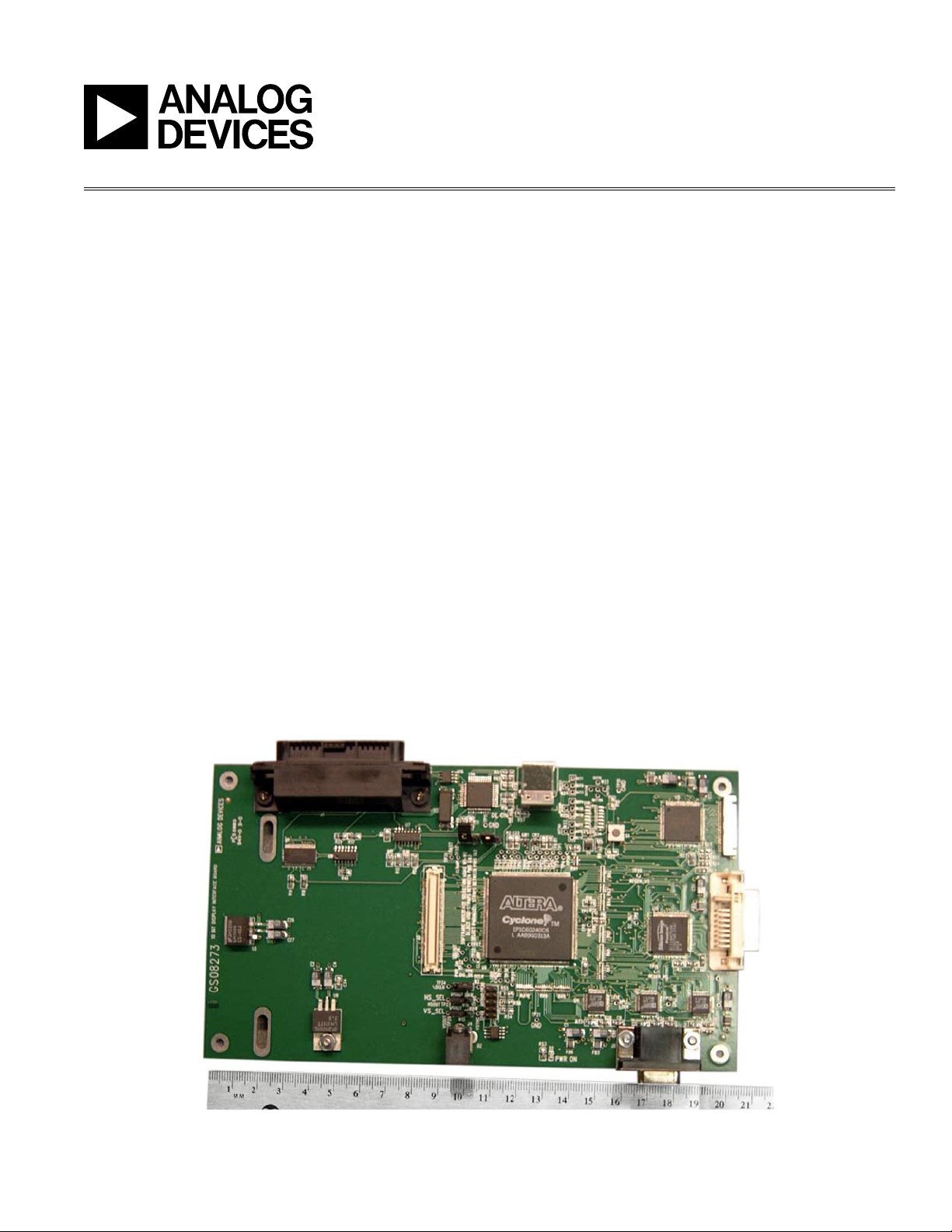
Figure 1. Board Shown in Centimeters
Page 2

AN-784
12
10
8
12
10
8
12
10
8
12
10
8
12
10
8
12
10
8
BLU A
BLU B
GRN A
GRN B
RED A
RED B
12
12
DAC
12
12
DAC
12
12
DAC
R
B
G
8 8 8 8 8 8
LVDS XMIT
WITH CONNECTOR
POWER
VGA CONN
FPGA
[DATA DEMUX
(SINGLE PORT MODE),
DE GENERATION,
DE CONTROL, COLOR
CONVERSION]
TMDS
XMIT
DIGITAL RGB
AND SYNCS
FROM AD988x
PARALLEL
INTFC CONN
USB
INTFC
SERIAL INTERFACE
SYNCS
TO FLAT PANEL
MONITOR
OR
LCD PROJECTOR
TO CRT
OR
FLAT PANEL
MONITOR
DVI CONNECTOR
TO TFT PANEL
05441-002
EVALUATION BOARD HARDWARE
POWER
This board is designed to receive 5 V dc through connector J4. The power supply that is included in the kit plugs
into this connector.
BOARD FUNCTIONS
A block diagram of the 10-bit display interface board
is shown in Figure 2. The following sections briefly
describe these functional blocks.
DATA DEMULTIPLEXING
The Altera EP1C6QC240 FPGA (U6) performs most of
the logic functions on the 10-bit display interface board.
Among these functions is the demultiplexing of the
digital RGB data output from the AD998x when it is in
single-port data output (30-bit) mode (the AD9981 and
AD9980 are 30-bit only). The DVI and LVDS transmitters, as well as the digital-to-analog converters (DACs),
require dual-port digital RGB data. Therefore, demultiplexing is required when in single-port mode.
DE GENERATION
The DVI and LVDS interfaces require a data enable (DE)
signal which indicates when there is active image data.
Since the analog graphics signal does not contain DE, the
FPGA on the 10-bit display interface board is required to
generate it. The duration of DE is programmable via the
10-bit DIB register map of the display electronics (DEPL)
evaluation software and supports any display resolution
up to 4096 pixels 4096 pixels.
COLOR SPACE CONVERSION
The FPGA contains circuitry to perform color space conversion for 30-bit YPbPr data. This can be enabled via the
10-bit DIB register map of the DEPL evaluation software.
This can be used in conjunction with the midscale clamp
feature on the analog interface of the AD998x devices to
provide the proper colors for an YPbPr video signal. The
color space conversion also works with YPbPr signals
transmitted over the DVI interface. For the most accurate
color space conversion, the conversion results in a 12-bit
output for each of the digital RGB output channels. This
minimizes the rounding errors that can result from the
conversion process.
Figure 2. 10-Bit Display Interface Board Block Diagram
–2–
REV. 0
Page 3
AN-784
05441-004
ANALOG
OUTPUT
5V
INPUT
DVI OUTPUT
LVDS OUTPUT
USB
INTERFACE
PARALLEL INTERFACE
ANALOG
INPUTS FOR
AD9981
DVI OUTPUT
The 10-bit display interface board provides a DVI output
via SiI160 transmitter (U15) and DVI-I connector (J8).
This can be connected via DVI cable to any display
device (flat panel monitor or LCD projector) to display
any image from VGA to UXGA-60 (the SiI160 is limited
to 25 MHz to 165 MHz operation). Note that the SiI160 is
capable of processing only 8-bit data. Therefore, only
the 8 MSBs of the data output from the FPGA are used
for the DVI output.
LVDS OUTPUT
The 10-bit display interface board provides an LVDS
output via DS90C387 transmitter (U5) and LVDS data
connector (J9). This can be connected via user-provided
cable to any board flat panel with LVDS interface (such
as Samsung’s 21.3’’ UXGA panel, LTM213U3-L01-0, or
Sharp’s 18’’ SXGA panel, LQ181E1LW31) to display an
image using that panel’s native resolution. This interface
is capable of operating up to UXGA-75 (202.5 MHz). Note
that the DS90C387 is capable of processing only 8-bit
data. Therefore, only the 8 MSBs of the data output from
the FPGA are used for the DVI output.
ANALOG OUTPUT
The 10-bit display interface board provides an analog
output via high performance AD9753 DACs (U11 to U13)
and 15-pin VGA connector (J6). The AD9753 is a 12-bit
DAC that provides precision digital-to-analog conversion. Therefore, the analog output port is the best choice
to demonstrate the full 10-bit performance of the AD998x
devices. The analog output can be connected via VGA
cable to any display device (flat panel monitor, CRT, or
projector) to display any image from VGA to UXGA-75.
SERIAL BUS TO COMPUTER INTERFACE
(USB OR PRINTER PORT)
Some circuitry is needed in order to interface the AD998x
and the 10-bit display interface board’s serial register
interface with a computer. The 10-bit display interface
board provides both a USB and a parallel (printer) port
interface. The USB interface consists of a USB-B connector (J2), USB controller (U14), and an EEPROM (U16)
that contains board ID information. The circuitr y for the
printer port’s serial interface use U1 and U9, in addition
to the Centronix connector, J1.
POWER
The 10-bit display interface board has two voltage regulators that generate 1.5 V and 3.3 V for its own logic.
These voltages are regulated off of the 5 V input at J4.
The 5 V input is also routed to the AD998x evaluation
board interface connector (J3) to provide power for the
AD998x evaluation board.
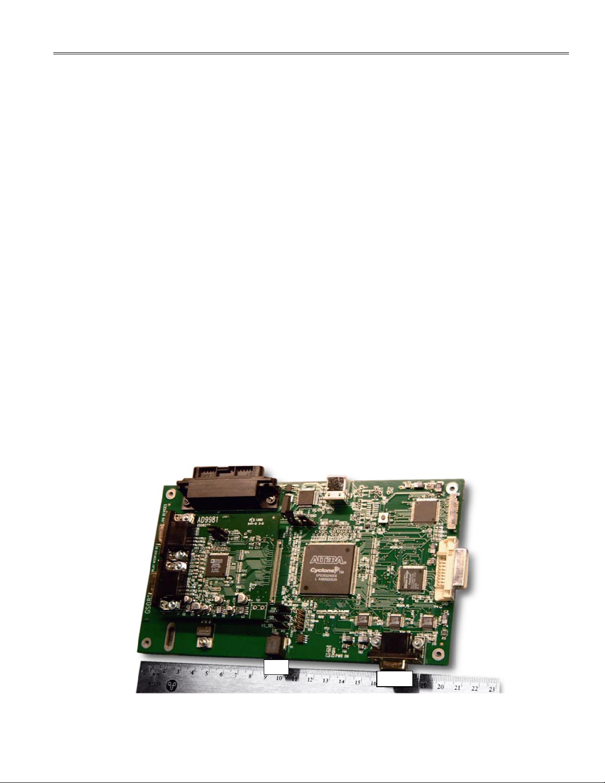
EVALUATION BOARD CONNECTIONS
Figure 3 shows how the 10-bit display interface board
interfaces with the AD9981 evaluation board. It also
indicates the various connections needed to evaluate
an image.
REV. 0
Figure 3. 10-Bit Display Interface Board with AD9981 Evaluation Board
–3–
Page 4

AN-784
CONFIGURING THE BOARD
DE Generation
The VS_SEL (W15 on schematic) and HS_SEL (W16 on
schematic) jumpers allow you to choose raw VSYNC and
HSYNC or the VSOUT and HSOUT outputs of the AD998x
to generate DE. If the jumpers are placed between Pins
1 and 2 (closer to U2), the raw HSYNC and VSYNC are
selected. If the jumpers are placed between Pins 2 and
3, the sync outputs (HSOUT and VSOUT) of the AD998x
are selected. Either configuration works, although the
HSYNC and VSYNC delay values used for DE generation
vary slightly in each case.
PC Port Selection
The jumpers at W1 and W2 must be configured appropriately to use the desired PC port for software control. To
select USB, the jumpers must be placed between Pins 2
and 3. To select the printer port, the jumpers should be
placed between Pin 1 and Pin 2.
To USB Driver Installation
Follow these steps to install the USB drivers on your
PC:
1. Connect the board to the power supply.
2. Connect the USB cable from the PC to the board.
3. Windows sees the new device and asks to install
drivers for it.
4. Select Search for Drivers and click Next.
5. Specify a location and browse on the CD-ROM to
the USB Drivers\win2k directory.
6. Click Next and follow any remaining instructions.
7. If asked for any files, always browse to the same
USB Drivers\ win2k (or \win98) folder to find them.
DCLK Selection
The 10-bit display interface board is configured so that
the DCLK output of the AD998x drives the generation
of PANEL_DCLK and PANEL_DE. This is accomplished
through the placement of a jumper bet ween Pins 1 and
2 of Header W3.
–4–
REV. 0
Page 5
AN-784
05441-003
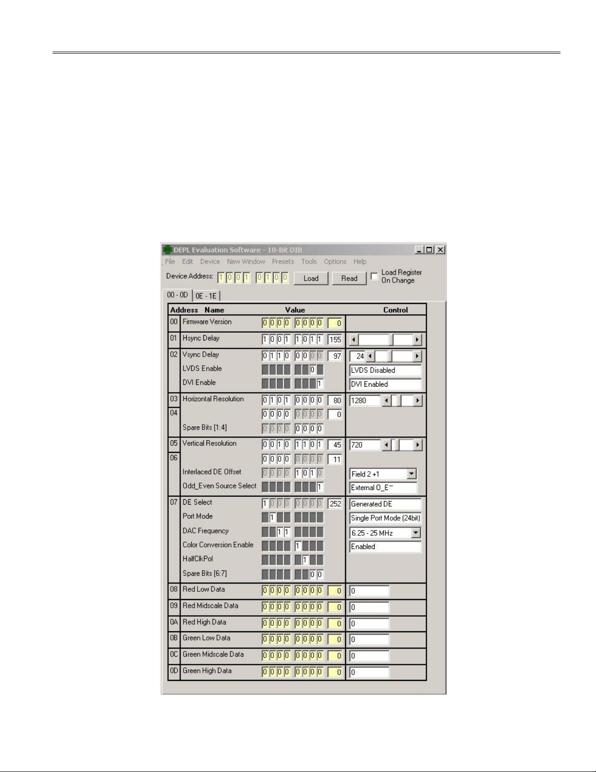
EVALUATION BOARD SOFTWARE
The 10-bit display interface board (DIB) registers can be
controlled using the 10-bit DIB register map of the DEPL
evaluation software. This software is a Visual Basic®
program requiring a Windows® 95, or later, operating
system. It is on a self-installing CD package included with
the evaluation board (in the \DEPL Evaluation Software
subdirector y). The 10-bit DIB register map of the DEPL
evaluation software should be loaded into the \Program
Files\ADI Software directory upon completion of a successful installation.
Note : If a DriverX Install error is encountered during
the software installation, rerun the driverxinstall.exe
program located in the Program Files\Analog Devices\
DEPL Evaluation Software\ DriverX directory.
The 10-bit DIB register map can be accessed two ways.
From the menu bar, sele ct Device > 10 Bit DIB. The
10-bit DIB register map can also be accessed by selection
Tools > 10- Bit Display Interfa ce Board Conf igur ation. The 10-bit DIB register map is shown in Figure 4.
Using this screen, the user can control the features of the
10-bit DIB.
To implement the controls, click Load. This is true unless
the Load Register on Change box is checked or the Read
button is clicked. In this case, the registers are updated
as soon as any change is made in the window.
REV. 0
Figure 4. Display Interface Board Configuration Setup Window
–5–
Page 6

AN-784
10-BIT DIB REGISTER DESCRIPTIONS
Hsync Delay (01–7:0)
Register 01 controls the number of data clock cycles that
occur between Hsync and the beginning of DE. This is a
decimal number that is written to an 8-bit register. For
ease of use, a sliding bar is also included as an alternative method for controlling the Hsync delay. Moving the
bar to the right increases the delay and is reflected in
the box to the right. Moving the bar left decreases the
delay.
If using the DVI output of the 10-bit display interface
board, note that an image might not be visible until the
Hsync Delay is near the appropriate amount of delay
from Hsync to active video.
Vsync Delay (02–7:2)
Bits 7:2 of Regis ter 02 control the number of Hsync
periods that occur between Vsync and the beginning of
DE. This is a decimal number that is written to a 6-bit
register. A sliding bar is also included for Vsync delay
control.
LVDS/DVI Interface Enable (02–1:0)
Bits 1:0 of Register 02 serve as enable bits to turn on the
LVDS and DVI interface outputs of the 10-bit DIB. It is
recommended that these interfaces be powered down
when not in use.
Horizontal Resolution (03–7:04–4)
Horizontal resolution must be set using the 12 bits spanning Register 3, Bit 7 (MSB) to Register 4, Bit 4 (LSB).
The resolution is set in number of pixels by typing the
decimal number directly into the text box on the right or
by moving the scroll bar next to it. The maximum value
is 4096.
Vertical Resolution (05–7:06–4)
Vertical resolution must be set using the 12 bits spanning Register 5, Bit 7 (MSB) to Register 6, Bit 4 (LSB).
The resolution is set in number of lines by typing the
decimal number directly into the text box on the right or
by moving the scroll bar next to it. The maximum value
is 4096.
DE Settings for Interlaced Video (06–3:0)
When generating a data enable (DE) from an interlaced
video source, it is necessary to provide for an offset
between the odd and even fields. Bits 3:1 of Register 6
allow you to program the amount of offset (in number of
lines) between the two fields. Bit 0 allows you to select
how the even and odd fields are differentiated from each
other. The AD998x devices have an ODD_EVEN~ signal
that is routed to the 10-bit DIB’s FPGA and can be used to
determine the differentiation by setting this bit to a Logic
1. If using a device that does not provide this signal, the
FPGA generates its own signal to provide this function.
This signal can be selected by setting Bit 0 to Logic 0.
DE Select (07–7)
This bit allows you to select the source for data enable
generation. If the analog interface of the AD998x is being
used, Generated DE must be selected since the analog
interface does not include a DE signal. If the DVI interface of the AD998x is being used, either Generated DE
of Digital DE can be used. However, it is recommended
that the Digital DE be selected in this case.
Port Mode (07–6)
This bit allows the user to select the operating mode of
the AD998x. If the AD998x is operating in single-channel
(30-bit) output mode (the AD9981 and the AD9980 have
single-channel output only), single port mode must be
selected. If the AD998x is operating in dual-channel (60bit) output mode, Dual Por t (60 bit) must be selected.
DAC Frequency (07–5:4)
From the DAC Frequency Range menu, you can select
the operating range of the analog output. The 12 MHz to
100 MHz range should be adequate to display all resolutions XGA and above (including 720p and 1080p). For
lower speed resolutions, the appropriate range should
be selected.
Color Conversion Enable (07–3)
The color conversion enable bit allows you to turn on the
30-bit color space converter in the FPGA.
Half Clock Invert (07–2)
The bit allows the user to route the first pixel of demultiplexed 30-bit data to the even output por t of the FPGA
rather than the odd output port. The timing relation
between data and the data clock (PANEL_CLK_OUT)
remain the same. This bit is useful when centering the
image using the Hsync delay register.
PC Port Selection
To select between the USB and parallel ports for the
software interface click on the Options pull-down menu
and click on Device Interface and then select either USB
or Parallel. Refer to the PC Port Selection section for
further setup instructions.
–6–
REV. 0
Page 7
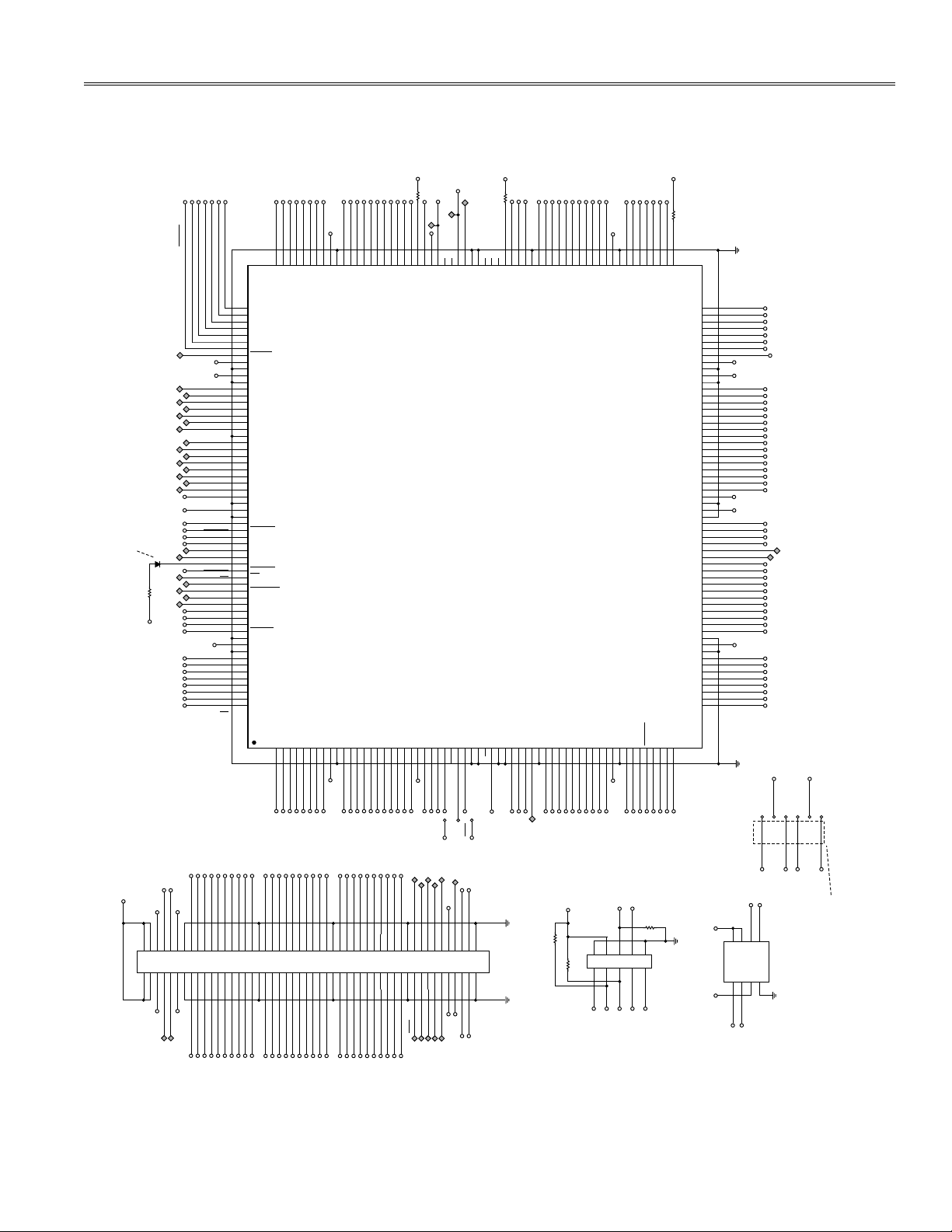
SCHEMATICS AND LAYOUT
61
62
63
64
65
66
67
68
69
70
71
72
73
74
75
76
77
78
79
80
81
82
83
84
85
86
87
88
89
90
91
92
93
94
95
96
97
98
99
100
101
102
103
104
105
106
107
108
109
110
111
112
113
114
115
116
117
118
119
120
REDA_IN8
REDA_IN9
REDB_IN0
REDB_IN1
REDB_IN2
REDB_IN3
REDB_IN4
REDB_IN5
3.3V
1.5V
REDB_IN6
REDB_IN7
REDB_IN8
REDB_IN9
HSYNC_IN
VSYNC_IN
DIG_DE
ODD_EVEN~
DAC_DIV1
DAC_DIV0
SPARE1
SPARE2
RED_ODD0
RED_ODD1
RED_ODD2
RED_ODD3
1.5V
3.3V
RED_ODD4
RED_ODD5
RED_ODD6
RED_ODD7
RED_ODD8
RED_ODD9
RED_ODD10
RED_ODD11
RED_EVEN0
RED_EVEN1
RED_EVEN2
RED_EVEN3
RED_EVEN4
RED_EVEN5
RED_EVEN6
RED_EVEN7
1.5V
3.3V
RED_EVEN8
RED_EVEN9
RED_EVEN10
RED_EVEN11
GRN_ODD0
GRN_ODD1
GRN_ODD2
GRN_ODD3
REDA_IN8
REDA_IN9
REDB_IN0
REDB_IN1
REDB_IN2
REDB_IN3
REDB_IN4
REDB_IN5
GND4
VCCIO4
GND5
VCCINT1
REDB_IN6
REDB_IN7
REDB_IN8
REDB_IN9
HSYNC_IN
VSYNC_IN
DIG_DE
ODD_EVEN~
DAC_DIV1
DAC_DIV0
SPARE_IO2
SPARE_IO3
RED_ODD0
RED_ODD1
RED_ODD2
RED_ODD3
GND6
VCCINT2
GND7
VCCIO5
RED_ODD4
RED_ODD5
RED_ODD6
RED_ODD7
RED_ODD8
RED_ODD9
RED_ODD10
RED_ODD11
RED_EVEN0
RED_EVEN1
RED_EVEN2
RED_EVEN3
RED_EVEN4
RED_EVEN5
RED_EVEN6
RED_EVEN7
GND8
VCCINT3
GND9
VCCIO6
RED_EVEN8
RED_EVEN9
RED_EVEN10
RED_EVEN11
GRN_ODD0
GRN_ODD1
GRN_ODD2
GRN_ODD3
TP38
TP37
1
1
123456789
101112131415161718192021222324252627282930313233343536373839404142434445464748495051525354555657585960
BLUB_IN0
BLUB_IN1
BLUB_IN2
BLUB_IN3
BLUB_IN4
BLUB_IN5
BLUB_IN6
BLUB_IN7
3.3V
BLUB_IN8
BLUB_IN9
GRNA_IN0
GRNA_IN1
GRNA_IN2
GRNA_IN3
GRNA_IN4
GRNA_IN5
GRNA_IN6
GRNA_IN7
GRNA_IN8
3.3V
GRNA_IN9
ALT_CSO
ALT_DATA
ALT_NCONFIG
DCLK_IN
SCL
ALT_NCE
ALT_DCLK
ALT_ASDO
SDA
SPARE23
GRNB_IN0
GRNB_IN1
GRNB_IN2
GRNB_IN3
GRNB_IN4
GRNB_IN5
GRNB_IN6
GRNB_IN7
GRNB_IN8
GRNB_IN9
3.3V
REDA_IN0
REDA_IN1
REDA_IN2
REDA_IN3
REDA_IN4
REDA_IN5
REDA_IN6
REDA_IN7
BLUB_IN0
BLUB_IN1
BLUB_IN2
BLUB_IN3
BLUB_IN4
BLUB_IN5
BLUB_IN6
BLUB_IN7
VCCIO1
GND1
BLUB_IN8
BLUB_IN9
GRNA_IN0
GRNA_IN1
GRNA_IN2
GRNA_IN3
GRNA_IN4
GRNA_IN5
GRNA_IN6
GRNA_IN7
GRNA_IN8
VCCIO2
GRNA_IN9
NCSO
DATA0
NCONFIG
VCCPLL1
DCLK_IN_CLK0
SCL_CLK1
GNDA_PLL1
GNDB_PLL1
NCEO
NCE
MSEL0
MSEL1
DCLK
ASDO
SDA
SPARE_IO1
GND2
GRNB_IN0
GRNB_IN1
GRNB_IN2
GRNB_IN3
GRNB_IN4
GRNB_IN5
GRNB_IN6
GRNB_IN7
GRNB_IN8
GRNB_IN9
VCCIO3
GND3
REDA_IN0
REDA_IN1
REDA_IN2
REDA_IN3
REDA_IN4
REDA_IN5
REDA_IN6
REDA_IN7
DCLK
DCLK
1
TP47
W3
R6
0�
180
179
178
177
176
175
174
173
172
171
170
169
168
167
166
165
164
163
162
161
160
159
158
157
156
155
154
153
152
151
150
147
146
145
144
143
142
141
140
139
138
137
136
135
134
133
132
131
130
129
128
127
126
125
124
123
122
121
BLU_EVEN5
BLU_EVEN4
BLU_EVEN3
BLU_EVEN2
BLU_EVEN1
BLU_EVEN0
PNL_CLK_LVDS
BLU_ODD11
BLU_ODD10
BLU_ODD9
BLU_ODD8
BLU_ODD7
BLU_ODD6
BLU_ODD5
BLU_ODD4
BLU_ODD3
BLU_ODD2
BLU_ODD1
BLU_ODD0
CLK_DVI
DVI_EN
3.3V
PANEL_CLK_OUT
PANEL_CLK_IN
SPARE_CLK
ALT_STATUS
ALT_CFG_DN
GRN_EVEN11
GRN_EVEN10
GRN_EVEN9
GRN_EVEN8
GRN_EVEN7
GRN_EVEN6
GRN_EVEN5
GRN_EVEN4
GRN_EVEN3
GRN_EVEN2
GRN_EVEN1
GRN_EVEN0
GRN_ODD11
3.3V
GRN_ODD10
GRN_ODD9
GRN_ODD8
GRN_ODD7
GRN_ODD6
GRN_ODD5
GRN_ODD4
CLK_ALG
BLU_EVEN5
BLU_EVEN4
BLU_EVEN3
BLU_EVEN2
BLU_EVEN1
BLU_EVEN0
PNL_CLK_LVDS
BLU_ODD11
VCCIO9
GND12
BLU_ODD10
BLU_ODD9
BLU_ODD8
BLU_ODD7
BLU_ODD6
BLU_ODD5
BLU_ODD4
BLU_ODD3
BLU_ODD2
BLU_ODD1
BLU_ODD0
PNL_CLK_DVI
DVI_EN
VCCIO8
PNL_CLK_OUT
TDI
VCCA_PLL2
PNL_CLK_IN_CLK2
SPARE_CLK3
GNDA_PLL2
GNDG_PLL2
TCK
NSTATUS
CONF_DONE
GRN_EVEN11
GRN_EVEN10
GND11
GRN_EVEN9
GRN_EVEN8
GRN_EVEN7
GRN_EVEN6
GRN_EVEN5
GRN_EVEN4
GRN_EVEN3
GRN_EVEN2
GRN_EVEN1
GRN_EVEN0
GRN_ODD11
VCCIO7
GND10
GRN_ODD10
GRN_ODD9
GRN_ODD8
GRN_ODD7
GRN_ODD6
GRN_ODD5
GRN_ODD4
PNL_CLK_ALG
3.3V
149
148
TDO
TMS
TP2
TP7
1
TP18
3.3V
R58
10k
�
PNL_CLK_ALG
240
239
238
237
236
235
234
233
232
231
230
229
228
227
226
225
224
223
222
221
220
219
218
217
216
215
214
213
212
211
210
209
208
207
206
205
204
203
202
201
200
199
198
197
196
195
194
193
192
191
190
189
188
187
186
185
184
183
182
181
RST
BLUA_IN9
BLUA_IN8
BLUA_IN7
BLUA_IN6
BLUA_IN5
BLUA_IN4
BLUA_IN3
3.3V
1.5V
BLUA_IN2
BLUA_IN1
BLUA_IN0
SPARE22
SPARE21
SPARE20
SPARE19
SPARE18
RST
PANEL
_
EN
SPARE17
SPARE16
DE_DETECT1
DE_DETECT2
LATCH_DE
LATCH
_
DE
1.5V
3.3V
SPARE15
SPARE14
SPARE13
SPARE12
SPARE11
SPARE10
SPARE9
SPARE8
SPARE7
SPARE6
SPARE5
REGEN_VS
SPARE4
REGEN_HS
DE_OUT
1.5V
3.3V
SPARE3
DEV_CLRN
BLUA_IN9
BLUA_IN8
BLUA_IN7
BLUA_IN6
BLUA_IN5
BLUA_IN4
BLUA_IN3
GND18
VCCIO12
GND17
VCCINT6
BLUA_IN2
BLUA_IN1
BLUA_IN0
SPARE_IO24
SPARE_IO23
SPARE_IO22
SPARE_IO21
SPARE_IO20
RST
PANEL_EN
SPARE_IO19
SPARE_IO18
DE_DETECT1
DE_DETECT2
LATCH_DE
LATCH_DE
GND16
VCCINT5
GND15
VCCIO11
SPARE_IO17
SPARE_IO16
SPARE_IO15
SPARE_IO14
SPARE_IO13
SPARE_IO12
SPARE_IO11
SPARE_IO10
SPARE_IO9
SPARE_IO8
SPARE_IO7
SPARE_IO6
SPARE_IO5
REGEN_VS
REGEN_HS
DE_OUT
GND14
VCCINT4
GND13
VCCIO10
SPARE_IO4
LVDS_EN
BLU_EVEN11
BLU_EVEN10
BLU_EVEN9
BLU_EVEN8
BLU_EVEN7
BLU_EVEN6
TP25
TP1
TP8
TP24
TP26
TP15
TP16
TP4
TP3
TP23
TP22
TP17
1
1
1
1
1
1
1
1
1
1
1
1
TP5
TP20
TP19
1
1
1
TP39
1
LVDS_EN
BLU_EVEN11
BLU_EVEN10
BLU_EVEN9
BLU_EVEN8
BLU_EVEN7
BLU_EVEN6
TP45
TP46
TP42
TP44
TP43
1
1
1
1
1
SMT_LED
D1
TP41
TP40
1
1
3.3V
10BIT_DIB_FPGA
EP1C6QC240
U6
ADD THIS TEXT TO
SILKSCREEN: "DE ON"
U6
MOLEX_52760-100
J3
ADD NET NAMES FOR ALL TPs (EXCEPT SPARES) TO SILKSCREEN
1
TP361TP35
1
TP30
1
TP28
1
TP331TP32
1
TP27
1
TP6
SOGOUT
ODD_EVEN~
VSOUT
DCLK
HSOUT
DIG_DE
CLAMP
135791113151719212325272931333537394143454749515355575961636567697173757779818385878991939597
99
246
8
101214161820222426283032343638404244464850525456586062646668707274767880828486889092949698
100
BLUA_IN8
BLUA_IN6
BLUA_IN5
REDA_IN9
REDA_IN8
NC
NC
NC
CTL3
CTL2
CTL0
PWR_DN
DCLK
CLK_INV
VSYNC
HSYNC
SCL
SDA
COAST
CTL1
NC
NC
NC
NC
BLUA_IN0
BLUB_IN0
BLUB_IN9
BLUB_IN8
BLUB_IN7
BLUB_IN6
BLUB_IN5
BLUB_IN4
BLUB_IN3
BLUB_IN2
BLUB_IN1
GRNB_IN6
GRNB_IN8
GRNB_IN9
GRNB_IN7
GRNB_IN5
GRNB_IN4
GRNB_IN3
GRNB_IN2
GRNB_IN1
GRNB_IN0
REDB_IN6
REDB_IN8
REDB_IN9
REDB_IN7
REDB_IN5
REDB_IN4
REDB_IN3
REDB_IN2
REDB_IN1
REDB_IN0
REDA_IN1
REDA_IN2
REDA_IN3
REDA_IN4
REDA_IN5
REDA_IN6
REDA_IN7
REDA_IN0
GRNA_IN6
GRNA_IN8
GRNA_IN9
BLUA_IN4
BLUA_IN3
BLUA_IN2
BLUA_IN1
GRNA_IN7
BLUA_IN7
BLUA_IN9
GRNA_IN0
GRNA_IN1
GRNA_IN2
GRNA_IN3
GRNA_IN4
GRNA_IN5
5V
1
TP31
1
TP29
1
TP341TP491TP48
13579
246
8
10
J7
ALT_CSO
ALT_NCONFIG
ALT_ASDO
ALT_DATA
ALT_DCLK
ALT_CFG_DN
3.3V
ALT_NCE
R56
10k
�
10k
�
R55
10k�
R54
EPCS1
U2
876
54
321
ALT_CSO
ALT_DATA
3.3V
ALT_ASDO
ALT_DCLK
3.3V
VCC3
VCC2
DCLK
ASDIGND
VCC1
DATA
NCS
VSOUT
RAW
RAW
HSOUT
HS_SEL VS_SEL
ADD THIS TEXT
TO SILKSCREEN
VSYNC
VSOUT
HSYNC
HSOUT
W15
W16
HSYNC_IN
VSYNC_IN
05441-005
PEV
R57
1k
�
R13
0�
PNL_CLK_DVI
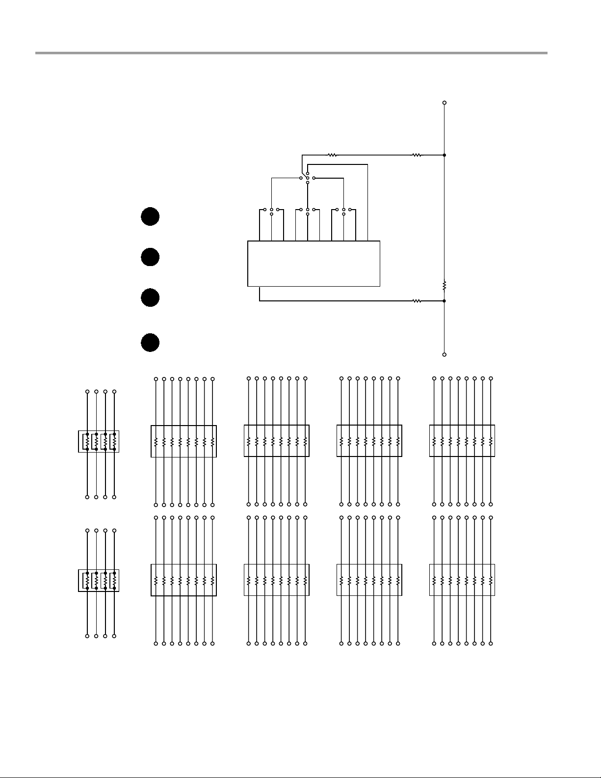
The schematics and layout for this board can also be found on the CD.
AN-784
REV. 0
Figure 5.
–7–
Page 8
AN-784
RA1 RA322 22
BLU_B8 BLU_A8
BLU_B9 BLU_A9
BLU_B10 BLU_A10
BLU_B11 BLU_A11BLU_EVEN11 BLU_ODD11
BLU_EVEN10 BLU_ODD10
BLU_EVEN9 BLU_ODD9
BLU_EVEN8 BLU_ODD8
RA5
RA7
RA9
RA2
RA6
RA8
RA10
22
22
22
22
22
22
22
1
1
1
1
1
1
1
16
16
16
16
16
16
16
GRN_EVEN11
GRN_ODD7
RED_EVEN3
BLU_EVEN7
GRN_EVEN3
RED_EVEN11
RED_ODD7
GRN_B11
GRN_A7
RED_B3
BLU_B7
GRN_B3
RED_B11
RED_A7
2
2
2
2
2
2
2
15
15
15
15
15
15
15
GRN_EVEN10
GRN_ODD6
RED_EVEN2
BLU_EVEN6
GRN_EVEN2
RED_EVEN10
RED_ODD6
GRN_B10
GRN_A6
RED_B2
BLU_B6
GRN_B2
RED_B10
RED_A6
3
3
3
3
3
3
3
14
14
14
14
14
14
14
GRN_EVEN9
GRN_ODD5
RED_EVEN1
BLU_EVEN5
GRN_EVEN1
RED_EVEN9
RED_ODD5
GRN_B9
GRN_A5
RED_B1
BLU_B5
GRN_B1
RED_B9
RED_A5
4
4
4
4
4
4
4
13
13
13
13
13
13
13
GRN_EVEN8
GRN_ODD4
RED_EVEN0
BLU_EVEN4
GRN_EVEN0
RED_EVEN8
RED_ODD4
GRN_B8
GRN_A4
RED_B0
BLU_B4
GRN_B0
RED_B8
RED_A4
5
5
5
5
5
5
5
12
12
12
12
12
12
12
GRN_EVEN7
GRN_ODD3
RED_ODD11
BLU_EVEN3
GRN_ODD11
RED_EVEN7
RED_ODD3
GRN_B7
GRN_A3
RED_A11
BLU_B3
GRN_A11
RED_B7
RED_A3
6
6
6
6
6
6
6
11
11
11
11
11
11
11
GRN_EVEN6
GRN_ODD2
RED_ODD10
BLU_EVEN2
GRN_ODD10
RED_EVEN6
RED_ODD2
GRN_B6
GRN_A2
RED_A10
BLU_B2
GRN_A10
RED_B6
RED_A2
7
7
7
7
7
7
7
10
10
10
10
10
10
10
GRN_EVEN5
GRN_ODD1
RED_ODD9
BLU_EVEN1
GRN_ODD9
RED_EVEN5
RED_ODD1
GRN_B5
GRN_A1
RED_A9
BLU_B1
GRN_A9
RED_B5
RED_A1
8
8
8
8
8
8
8
9
9
9
9
9
9
9
GRN_EVEN4
GRN_ODD0
RED_ODD8
BLU_EVEN0
GRN_ODD8
RED_EVEN4
RED_ODD0
RA4
22
1
16
BLU_ODD7
BLU_A7
2
15
BLU_ODD6
BLU_A6
3
14
BLU_ODD5
BLU_A5
4
13
BLU_ODD4
BLU_A4
5
12
BLU_ODD3
BLU_A3
6
11
BLU_ODD2
BLU_A2
7
10
BLU_ODD1
BLU_A1
8
9
BLU_ODD0
BLU_A0
GRN_B4
GRN_A0
RED_A8
BLU_B0
GRN_A8
RED_B4
RED_A0
PLACE MOUNTING HOLES IN
EACH CORNER OF THE PCB.
H1 H2 H3 H4
THE CLOCK DELAY CIRCUIT SHOWN
HERE IS A STUFFING OPT.
PLACE U10 AS CLOSE AS POSSIBLE TO U6.
KEEP THESE TRACES AS SHORT AS POSSIBLE.
IN
OUT1
OUT2
OUT3
OUT4
OUT5
OUT6
OUT7
OUT8
OUT9
OUT10
3D7110
GND; 7
PLACE NEAR
U6:174
PLACE NEAR
W23
R14
0Ω
PNL_CLK_LVDS2
PANEL_CLK_IN_DLY
PANEL_CLK_IN_DLY2
R22
0Ω
PANEL_CLK_LVDS1
PNL_CLK_LVDS
R20
0Ω
W25
W24
R15
22Ω
11
13
3
12
4
11
5
10
6
9
8
U10
3.3V; 14
W23
OUT10
OUT8
OUT789
OUT1
W22
OUT5
OUT6
OUT9
OUT7
OUT4
OUT3
OUT2
OUT123
OUT456
05441-006
Figure 6.
–8–
REV. 0
Page 9

AN-784
SII160
U15
3.3V; 8, 30, 56, 88
GND; 7, 19, 31, 33,37, 41
GND; 47, 57, 67, 79, 86, 89
RES1
RES2
RES3
RES4
CTL1
CTL2
TXC–
TXC+
TX0–
TX0+
TX1–
TX1+
TX2–
TX2+
EXT_SWING
PIXS
EDGE
IDCK
DE
VSYNC
HSYNC
BE[7:0]
GE[7:0]
RE[7:0]
BO[7:0]
RO[7:0]
GO[7:0]
IVCC4
IVCC3
IVCC2
IVCC1
AVCC3
AVCC2
AVCC1
PVCC2
PVCC1
CTL3
PD
RES5
RES6
RES7
RES8
GND; 3,11,15,19,22
DVI_AD
(VIEW FROM BOTTOM) J8
RXC+
RXC–
VSYC
HSYC
BLUE
GREN
RED
RX0–
RX0+
RX1+
RX1–
RX2+
RX2–
DDCSDA
DDCSCL
ROUTE THESE AS 50Ω DIFFERENTIAL PAIRS
EXT_SWING
PIXS
EDGE
DVI_EN
23
24
8
25
282726
17
18
10
9
2
1
7
6
DVI_TXC–
PNL_CLK_DVI
R8
510Ω
3.3V
DVI_TXC+
DVI_TX0–
84
83
34
35
39
40
42
43
45
46
32
26
25
24
80
78
77
76
[9:16]
[99:100], [1:6]
[90:97]
[68:75]
[48:55]
[58:65]
98
81
66
17
44
38
36
85
18
82
29
87
20
21
22
23
27
28
AVDD
R7
4.75kΩ
R3
4.75kΩ
3.3V
DVI_PVCC
AVDD
GRN_B[11:4]
RED_B[11:4]
BLU_B[11:4]
RED_A[11:4]
GRN_A[11:4]
BLU_A[11:4]
REGEN_HS
REGEN_VS
DE_OUT
DVI_TX2+
DVI_TX2–
DVI_TX1+
DVI_TX1–
DVI_TX0+
3.3V
05441-007
Figure 7.
REV. 0
–9–
Page 10

AN-784
1
101112131415161718
19
2
202122232425262728
29
3
30
31
45678
9
FI-WE31P-HF
J9
1
101112131415161718
19
2
202122232425262728
29
3
30
31
45678
9
TXOUT7+
TXOUT7–
TXOUT6+
TXOUT6–
TXOUT4–
TXOUT5+
TXOUT5–
TXOUT4+
TXOUTCLK+
TXOUTCLK–
TXOUT3–
TXOUT3+
TXOUT2+
TXOUT2–
TXOUT1+
TXOUT1–
TXOUT0+
TXOUT0–
A1M
A1P
A2M
A2P
A3M
A3P
A4M
A4P
A5M
A5P
A6M
A6P
A7M
A7P
AOM
AOP
B10
B11
B12
B13
B14
B15
B16
B17
B20
B21
B22
B23
B24
B25
B26
B27
BAL
CLK1M
CLK1P
CLK2M/NC
CLK2P/NC
CLKIN
DE
DUAL
G10
G11
G12
G13
G14
G15
G16
G17
G20
G21
G22
G23
G24
G25
G26
G27
HSYNC
PLLSEL
PRE
R10
R11
R12
R13
R14
R15
R16
R17
R20
R21
R22
R23
R24
R25
R26
R27
R_FB
R_FDE
VSYNC
PD
FROM FPGA
LVDS_EN
RED_A10
RED_A9
RED_A8
RED_A7
RED_A6
RED_A5
RED_A4
RED_B11
RED_B10
RED_B9
RED_B8
RED_B7
RED_B6
RED_B5
RED_B4
BLU_B11
BLU_B10
BLU_B9
BLU_B8
BLU_B7
BLU_B6
BLU_B5
BLU_B4
BLU_A11
BLU_A10
BLU_A9
BLU_A8
BLU_A7
BLU_A6
BLU_A5
BLU_A4
GRN_B11
GRN_B10
GRN_B9
GRN_B8
GRN_B7
GRN_B6
GRN_B5
GRN_B4
GRN_A11
GRN_A10
GRN_A9
GRN_A8
GRN_A7
GRN_A6
GRN_A5
GRN_A4
PNL_CLK_LVDS2
474645
44
393837363433323129
28
50
49
92
91
90
89
88
87
86
85
64
63
62
61
60
59
58
57
24
42
41
27
26
11
56
23
2
1
100
99
96
95
94
93
74
73
72
71
70
69
66
65
54
15
14
10
9
8
7
6
5
4
3
84
81
80
79
78
77
76
75
20
21
55
22
U5
DS90C387
GND; 13, 16, 17, 19, 25, 35, 51, 52, 43, 68, 83, 98
3.3V; 53, 67, 82, 97
LVPLL_VCC; 12, 18
LVDS_VCC; 30, 40, 48
R27
4.75kΩ
R26
4.75kΩ
R25
4.75kΩ
R24
4.75kΩ
R23
4.75kΩ
RED_A11
TXOUT0–
TXOUT0+
TXOUT1–
TXOUT1+
TXOUT2–
TXOUT2+
TXOUTCLK–
TXOUTCLK+
TXOUT3–
TXOUT3+
TXOUT4–
TXOUT4+
TXOUT5–
TXOUT5+
TXOUT6–
TXOUT6+
TXOUT7–
TXOUT7+
REGEN_HS
REGEN_VS
DE_OUT
PRE
3.3V
R_FB
R_FDE
DUAL
BAL
05441-008
LVDS OUTPUT CONNECTOR
Figure 8.
–10–
REV. 0
Page 11

AN-784
GND; 4, 22, 44, 45
AVDD
CLKVDD
DVDD1
DVDD2
IOUTA
IOUTB
PLLVDD
PLLLOCK
FSADJ
REFIO
LPF
DIV1
DIV0
CLK–
CLK+
RST
PORT1B[11:0]
PORT2B[11:0]
AD9753
U11
ACLKR
PLLVDD
RED_A[11:0]
41
48
21
5
43
42
47
6
40
39
46
38
37
3
2
1
[7:18]
[23:34]
PNL_CLK_ALG
C9
1µF
PLLVDD
R28
392Ω
R29
4.75kΩ
R33
75Ω
R32
37.4Ω
R31
2kΩ
C5
0.1µF
R30
4.75kΩ
1
TP12
3.3V
AVDD
RED_B[11:0]
DAC_DIV0
DAC_DIV1
RPLL_LOCK
ARED_OUT
ROUT–
RFSADJ
RREF
CLKVDD
GND; 4, 22, 44, 45
AVDD
CLKVDD
DVDD1
DVDD2
IOUTA
IOUTB
PLLVDD
PLLLOCK
FSADJ
REFIO
LPF
DIV1
DIV0
CLK–
CLK+
RST
PORT1B[11:0]
PORT2B[11:0]
AD9753
U12
ACLKG
PLLVDD
GRN_A[11:0]
41
48
21
5
43
42
47
6
40
39
46
38
37
3
2
1
[7:18]
[23:34]
PNL_CLK_ALG
C8
1µF
PLLVDD
R34
392Ω
R45
4.75kΩ
R37
75Ω
R36
37.4Ω
R35
2kΩ
C6
0.1µF
R44
4.75kΩ
1
TP13
3.3V
AVDD
GRN_B[11:0]
DAC_DIV0
DAC_DIV1
GPLL_LOCK
AGRN_OUT
GOUT–
GFSADJ
GREF
CLKVDD
GND; 4, 22, 44, 45
AVDD
CLKVDD
DVDD1
DVDD2
IOUTA
IOUTB
PLLVDD
PLLLOCK
FSADJ
REFIO
LPF
DIV1
DIV0
CLK–
CLK+
RST
PORT1B[11:0]
PORT2B[11:0]
AD9753
U13
ACLKB
PLLVDD
BLU_A[11:0]
41
48
21
5
43
42
47
6
40
39
46
38
37
3
2
1
[7:18]
[23:34]
PNL_CLK_ALG
C10
1µF
PLLVDD
R38
392Ω
R43
4.75kΩ
R41
75Ω
R40
37.4Ω
R39
2kΩ
C7
0.1µF
R42
4.75kΩ
1
TP14
3.3V
AVDD
BLU_B[11:0]
DAC_DIV0
DAC_DIV1
BPLL_LOCK
ABLU_OUT
BOUT–
BFSADJ
BREF
CLKVDD
CON-HD-15HM
ARED_OUT
AGRN_OUT
15
6
5
4
3
2
1
14
13
12
11
10
9
8
7
J6
ABLU_OUT
REGEN_HS
REGEN_VS
05441-009
Figure 9.
–11–
REV. 0
Page 12

AN-784
A1A0A2
VSS SDA
SCL
WP
VCC
24LCO4B
U16
GND6
D0D1D2
D3
D4
D5
D6
D7
BKPT
VCC2
PC0/RXD0
PC1/TXD0
PC2/INT0#
PC3/INT1#
PC4/T0
PC5/T1
PC6/WR#
PC7/RD#
VCC
AVCC
XOUT
XIN
AGND
GND4
GND3
GND2
GND1
CLK24
GND5
RESET
VCC1
VCC3
DISCON#
USBD+
USBD–
PA5/FRD#
PA4/FWR#
GND8
WAKEUP#
SCL
SDA
GND7
GND
AN2126SC
U14
XTAL2
XTAL1
GND; 5, 6
USB_A
GND
–DATA
+DATA
PWR_IN
1B4
1B3
1B2
1B1
2B1
2B2
2B3
2B4
S1S0
2OE1A2A
GND; 8
SN74CBLTV3253
3.3V; 16
1OE
36CRPX
J1
G19
G20
G21
G22
G23
G24
G25
G26
G27
G28
G29
G30
P1
P2
P3
P4
P5
P6
P32
P31
ENC11D 1Q
2D 2Q
5D
6D 6Q
4Q
5Q
7Q7D
8D 8Q
3D 3Q
4D
ENC11D 1Q
2D 2Q
5D
6D 6Q
4Q
5Q
7Q7D
8D 8Q
3D 3Q
4D
74VHC14 74VHC14
74VHC14
74VHC14
STROBE
FROM PC
3-STATE DATA LINE
1
NOTE: PLACE W1 AND W2 IN A ROW AND
ADD THIS TEXT TO THE SILKSCREEN.
SOFTWARE INTERFACE SELECTION USING W1-W2:
SELECT USB: STRAPS BETWEEN PINS 2 AND 3
SELECT PARALLEL: STRAPS BETWEEN PINS 1 AND 2
8
U9
10
11
U9
SCL_U
SCL_USB
2143
R52
4.75kΩ
R17
4.75kΩ
PAR_STRB
36 13
35 14
33 16
32 17
30 19
29 20
27 22
26 23
25
24
U1
LCX16374A
LCX16374A
GND; 4, 10, 15, 21,
28, 34, 39, 45
WR_EN
SER_DAT_2PC
SER_DAT_2BD
R46
2kΩ
R18
2kΩ
R21
2kΩ
3.3V
3.3V
R19
2kΩ
47246344543
6
38
371248
1
8119
40
41
U1
3.3V; 7, 18, 31, 42
19
20
21
22
23
24
25
262728
29
30
1
[33:36]
2
3
4
5
63231
[10:18]
SDA_PAR
3.3V
3.3V
SDA_SEL
SDA_USB
SCL_EE
SDA_EE
SCL_SEL
USB_SDA
3.3V
3.3V
USB_SCL
3
4
5
6
101112
13
2
14
15
791
U7
R47
24.3Ω
USBD
USBD
USB_DATA
USB_DATA
R50
2.21kΩ
123
4
J2
3.3V
R16
2.21kΩ
R51
1.5kΩ
R48
24.3Ω
C101
22pF
C102
22pF
2
1
X2
12MHz
CRYSTAL
C11
1µF
USBRST
R49
10kΩ
23
24
25
26
27
28
29
30
31
32
33
14
15
16
17
18
19
20
21
11
10
9
8
7
654
3
2
1
12
13
22
44
43
42
41
40
39
38
37
36
35
34
AVDD
XIN
XOUT
213
4
678
R5
10kΩ
R10
10kΩ
1 1
2 2
R12
10kΩ
R11
10kΩ
W2
W1
SCL_USB
SCL
SCL_PAR
SCL_PAR
SER_CLK
SDA_PAR
SDA
SDA_USB
5
3
2
1
3
2
CENTRONICS 36 PIN
PRINTER PORT CONNECTOR
SERIAL INTERFACE CIRCUIT
U9
U9
1 1
2 2
05441-010
9
Figure 10.
–12–
REV. 0
Page 13

AN-784
C4
C2
C34 C28 C36 C35 C31 C29 C30 C13 C40 C39 C43 C37 C44 C48 C45 C46 C47 C12 C42 C41 C56 C57 C58 C59 C55 C54
10µF
10µF
0.1µF 0.1µF 0.1µF 0.1µF 0.1µF 0.1µF 0.1µF 0.1µF 0.1µF 0.1µF 0.1µF 0.1µF 0.1µF 0.1µF 0.1µF 0.1µF 0.1µF 0.1µF 0.1µF 0.1µF 0.1µF 0.1µF 0.1µF 0.1µF 0.1µF 0.1µF
C76 C77 C78 C79 C80 C81 C82 C83 C84 C85 C86 C87 C88 C18 C20 C25 C89 C90 C19
0.1µF 0.1µF 0.1µF 0.1µF 0.1µF 0.1µF 0.1µF 0.1µF 0.1µF 0.1µF 0.1µF 0.1µF 0.1µF 0.1µF 0.1µF 0.1µF 0.1µF 0.1µF 0.1µF
++
2
V
OUT
V
IN
GND
1
3
1
1
1
1
TP10
TP9
TP21
TP11
R53
1kΩ
D2
SMT_LED
ADD TEXT TO
SILKSCREEN: "PWR ON"
C27 C16 C15 C23 C24 C22 C21
10µF 0.1µF 0.1µF 0.1µF 0.1µF 0.1µF 0.1µF
3.3V
3.3V
LM1085IT
+
U8
2
V
OUT
V
IN
GND
1
3
1.5V
ADJ
LM1086CS
U3
2
J4
+
C26
10µF
C17 C61 C62 C63 C64 C60 C65 C95
0.1µF 0.1µF 0.1µF 0.1µF 0.1µF 0.1µF 0.1µF 0.1µF
C49
10µF
+
1
2
FB1
MHz
AVDD
C96
C98
0.1µF
0.1µF
C50
10µF
C51
10µF
+
+
1
1
2
2
FB3
FB2
MHz
MHz
PLLVDD
DVI_PVCC
C69
C66
C68
C67
0.1µF
0.1µF
0.1µF
0.1µF
C99
C97
0.1µF
0.1µF
C52
10µF
C53
10µF
+
+
1
1
2
2
FB5
FB4
MHz
MHz
LVDS_VCC
LVPLL_VCC
C72
C74
C71
C75
0.1µF
0.1µF
0.1µF
0.1µF
ANALOG SUPPLY
FOR DACS AND
DVI TRANSMITTER
C73
0.1µF
C70
0.1µF
DAC PLL SUPPLY
DVI PLL SUPPLY
LVDS SUPPLY
LVDS PLL SUPPLY
DAC CLK SUPPLY
10µF
C1
CLKVDD
3.3V
C104
0.1µF
0.1µF
C103
0.1µF
C38
0.1µF
C3
1
2
FB6
MHz
+
HSMS-2814
R2
10kΩ
1
2
3
CR1
C33
1µF
LATCH_DE
DE_DETECT1
HSMS-2814
1
2
R1
10kΩ
1
2
3
CR2
C32
1µF
LATCH_DE
DE_DETECT2
1
GND
SRT
VCC
RST
LP3470
U4
VCC1
POWER-ON RESET
SRT
RST_PWR
2
1
4
5
3
R4
1kΩ
C14
0.1µF
S1
PB_SW
R9
2kΩ
RST
3.3V
3.3V
2
05441-011
5V
R59
121Ω
R60
24.3Ω
1
2
REV. 0
Figure 11.
–13–
Page 14

AN-784
05441-012
Figure 12.
–14–
REV. 0
Page 15

AN-784
05441-013
REV. 0
Figure 13.
–15–
Page 16

AN-784
05441-014
Figure 14.
–16–
REV. 0
Page 17

AN-784
05441-015
REV. 0
Figure 15.
–17–
Page 18

AN-784
05441-016
Figure 16.
–18–
REV. 0
Page 19

AN-784
05441-017
REV. 0
Figure 17.
–19–
Page 20

–20–
Page 21

–21–
Page 22

–22–
Page 23

–23–
Page 24

AN05481–0– 4/05(0)
© 2005 Analog Devices, Inc. All rights reserved. Trademarks and registered trademarks are the property of their respective owners.
–24–
 Loading...