

Page 1
■ Overview
The AN77L00/AN77L00M series is a stabilized constant
voltage power supply with a low input/output voltage(0.3V
max.). It is suitable for the low-voltage equipment using
batteries, and consumer/industrial equipment with great
fluctuation of the supply voltage.
A wide range of output voltage is available from 3V
through 10V.
■ Features
• Minimum input/output voltage difference : 0.3V(max.)
• Built-in overcurrent limiting circuit
• Built-in rush current preventive circuit at saturation volt-
age rise time
• Built-in overheat protective circuit
• Built-in input short-circuit protective circuit
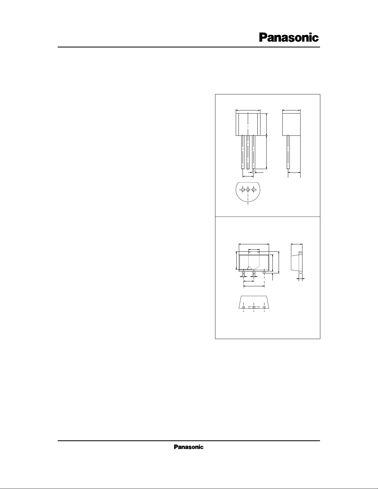
1
Voltage Regulators
AN77L00/AN77L00M Series
3-pin Low Power Loss Voltage Regulato r(100mA Type)
AN77L00 Series
Unit : mm
5.0
±0.2
2.3±0.2
5.1±0.213.5±0.5
0.45
+0.2
– 0.1
2.54
4.0±0.2
213
3-pin SIL Plastic Package (TO-92) (SSIP003-P-0000)
AN77L00M Series Unit : mm
3-pin SIL Mini Power Type Plastic Package (TO-220F) (SSIP003-P-0000D)
4.6max.
1.6max.
0.44max.
0.48max.
1.8max.
1.5
3.0
2.6max.
4.25max.
0.8min.
2.6
0.58max.
4.5
123
Page 2

2
Voltage Regulators
AN77L00/AN77L00M Series
3 12
–
+
IN
(1)
GND
(3)
OUT
(2)
The pin numbers in are for the AN77L00M series.
The pin numbers in ( ) are for the AN77L00 series.
Error Amp.
Starter
Voltage
Reference
Input Short-Circuit
Protection
Over Current
Protection
Over Current
Protection
Rush Current
Protection
Thermal
Protection
■ Block Diagram
V
IN
I
IN
P
D
T
opr
T
stg
Supply voltage
Supply current
Power dissipation
Note1)
Operating ambient temperature
Storage temperature
V
mA
mW
˚C
˚C
Parameter Symbol Rating Unit
■ Absolute Maximum Ratings (Ta=25˚C)
30
200
650
–30 to + 85
–55 to + 150
Note 1)
Part No. Output voltage (VO) Operating supply voltage range (VI)
■ Recommended Operating Range (Ta= 25˚C)
AN77L03/M
AN77L035/M
AN77L04/M
AN77L045/M
AN77L05/M
AN77L06/M
AN77L07/M
AN77L08/M
AN77L09/M
AN77L10/M
AN77L12/M
3
3.5
4
4.5
5
6
7
8
9
10
12
VO + 0.3 to 13.62
VO + 0.41 to 14.14
VO + 0.3 to 14.66
VO + 0.43 to 15.18
VO + 0.3 to 15.7
VO + 0.46 to 16.74
VO + 0.48 to 17.78
VO + 0.51 to 18.82
VO + 0.53 to 19.86
VO + 0.55 to 20.9
VO + 0.6 to 22.98
V
V
V
V
V
V
V
V
V
V
V
Unit
Page 3
3
Voltage Regulators
AN77L00/AN77L00M Series
Output voltage
Input stability
Load stability
Bias current under no load
Bias current fluctuation under load
Bias current before regulation start
Ripple rejection ratio
Min. input/output voltage difference (1)
Min. input/output voltage difference (2)
Output noise voltage
Output voltage temperature coefficient
V
O
REG
IN
REG
L
I
bias
∆I
bias
I
rush
RR
V
DIF (min) 1
V
DIF (min) 2
V
no
∆VO/Ta
Tj=25˚C
V
I
=3.62 to 13.62V, Tj=25˚C
I
O
=0 to 100mA, Tj=25˚C
I
O
=0mA, Tj=25˚C
I
O
=0 to 100mA, Tj=25˚C
V
I
=2.7V, IO=0mA, Tj=25˚C
V
I
=3.62 to 5.62V, f=120Hz
V
I
=2.7V, IO=50mA, Tj=25˚C
V
I
=2.7V, IO=100mA, Tj=25˚C
f=10Hz to 100kHz
T
j
= –30 to+125˚C
2.88
60
3
2
8
0.9
3
1.5
70
0.12
0.22
70
0.2
3.12
60
60
1.5
5
5
0.25
0.3
V
mV
mV
mA
mA
mA
dB
V
V
µV
mV/˚C
Parameter Symbol Condition min typ max Unit
■ Electrical Characteristics (Ta=25˚C)
• AN77L03/M (3V, 100mA Type)
Note 1) Under Tj=25˚C, each test duration can be set short (within 10ms) and the characteristic drift with temperature rise at
joints of the chip may be ignored.
Note 2) VI=4V, IO=50mA, CO=10µF unless otherwise specified.
Output voltage
Input stability
Load stability
Bias current under no load
Bias current fluctuation under load
Bias current before regulation start
Ripple rejection ratio
Min. input/output voltage difference (1)
Min. input/output voltage difference (2)
Output noise voltage
Output voltage temperature coefficient
T
j
=25˚C
V
I
= 4.14 to 14.14V, Tj=25˚C
I
O
= 0 to 100mA, Tj= 25˚C
I
O
= 0mA, Tj= 25˚C
I
O
= 0 to 100mA, Tj= 25˚C
V
I
= 3.15V, IO= 0mA, Tj=25˚C
V
I
= 4.14 to 6.14V, f=120Hz
V
I
= 3.15V, IO= 50mA, Tj= 25˚C
V
I
= 3.15V, IO=100mA, Tj= 25˚C
f=10Hz to 100kHz
T
j
= –30 to+125˚C
3.36
59
3.5
3
9
0.9
3
1.5
69
0.12
0.22
75
0.23
3.64
60
60
1.5
5
5
0.25
0.41
Parameter Symbol Condition min typ max Unit
•
AN77L035/M (3.5V, 100mA Type)
Note 1) Under Tj=25˚C, each test duration can be set short (within 10ms) and the characteristic drift with temperature rise at
joints of the chip may be ignored.
Note 2) VI=4.5V, IO=50mA, CO=10µF unless otherwise specified.
V
O
REG
IN
REG
L
I
bias
∆I
bias
I
rush
RR
V
DIF (min) 1
V
DIF (min) 2
V
no
∆VO/Ta
V
mV
mV
mA
mA
mA
dB
V
V
µV
mV/˚C
Output voltage
Input stability
Load stability
Bias current under no load
Bias current fluctuation under load
Bias current before regulation start
Ripple rejection ratio
Min. input/output voltage difference (1)
Min. input/output voltage difference (2)
Output noise voltage
Output voltage temperature coefficient
T
j
=25˚C
V
I
= 4.66 to 14.66V, Tj= 25˚C
I
O
= 0 to 100mA, Tj= 25˚C
I
O
= 0mA, Tj= 25˚C
I
O
= 0 to 100mA, Tj=25˚C
V
I
=3.6V, IO= 0mA, Tj= 25˚C
V
I
= 4.66 to 6.66V, f=120Hz
V
I
=3.6V, IO=50mA, Tj= 25˚C
V
I
=3.6V, IO=100mA, Tj= 25˚C
f=10Hz to 100kHz
T
j
= –30 to+125˚C
3.84
59
4
3
9
0.9
3
1.5
69
0.12
0.23
80
0.26
4.16
60
60
1.5
5
5
0.25
0.3
Parameter Symbol Condition min typ max Unit
•
AN77L04/M (4V, 100mA Type)
Note 1) Under Tj=25˚C, each test duration can be set short (within 10ms) and the characteristic drift with temperature rise at
joints of the chip may be ignored.
Note 2) VI=5V, IO=50mA, CO=10µF unless otherwise specified.
V
O
REG
IN
REG
L
I
bias
∆I
bias
I
rush
RR
V
DIF (min) 1
V
DIF (min) 2
V
no
∆VO/Ta
V
mV
mV
mA
mA
mA
dB
V
V
µV
mV/˚C
Page 4

4
Voltage Regulators
AN77L00/AN77L00M Series
Output voltage
Input stability
Load stability
Bias current under no load
Bias current fluctuation under load
Bias current before regulation start
Ripple rejection ratio
Min. input/output voltage difference (1)
Min. input/output voltage difference (2)
Output noise voltage
Output voltage temperature coefficient
T
j
=25˚C
V
I
=5.18 to 15.18V, Tj=25˚C
I
O
= 0 to 100mA, Tj=25˚C
I
O
= 0mA, Tj=25˚C
I
O
= 0 to 100mA, Tj=25˚C
V
I
= 4.05V, IO= 0mA, Tj=25˚C
V
I
=7.18 to 6.18V, f=120Hz
V
I
= 4.05V, IO=50mA, Tj=25˚C
V
I
= 4.05V, IO=100mA, Tj=25˚C
f=10Hz to 100kHz
T
j
= –30 to+125˚C
4.32
58
4.5
3
10
0.9
3
1.5
68
0.12
0.23
85
0.3
4.68
60
60
1.5
5
5
0.25
0.43
Parameter Symbol Condition min typ max Unit
■ Electrical Characteristics (Ta=25˚C)
• AN77L045/M (4.5V, 100mA Type)
Note 1) Under Tj=25˚C, each test duration can be set short (within 10ms) and the characteristic drift with temperature rise at
joints of the chip may be ignored.
Note 2) VI=5.5V, IO=50mA, CO=10µF unless otherwise specified.
V
O
REG
IN
REG
L
I
bias
∆I
bias
I
rush
RR
V
DIF (min) 1
V
DIF (min) 2
V
no
∆VO/Ta
V
mV
mV
mA
mA
mA
dB
V
V
µV
mV/˚C
Output voltage
Input stability
Load stability
Bias current under no load
Bias current fluctuation under load
Bias current before regulation start
Ripple rejection ratio
Min. input/output voltage difference (1)
Min. input/output voltage difference (2)
Output noise voltage
Output voltage temperature coefficient
T
j
=25˚C
V
I
=5.7 to 15.7V, Tj=25˚C
I
O
= 0 to 100mA, Tj=25˚C
I
O
= 0mA, Tj=25˚C
I
O
= 0 to 100mA, Tj=25˚C
V
I
= 4.5V, IO= 0mA, Tj=25˚C
V
I
= 5.7 to 7.7V, f=120Hz
V
I
= 4.5V, IO= 50mA, Tj=25˚C
V
I
= 4.5V, IO= 100mA, Tj=25˚C
f=10Hz to 100kHz
T
j
= –30 to+125˚C
4.8
58
5
4
10
0.9
3
1.5
68
0.12
0.24
90
0.33
5.2
60
60
1.5
5
5
0.25
0.3
Parameter Symbol Condition min typ max Unit
• AN77L05/M (5V, 100mA Type)
Note 1) Under Tj=25˚C, each test duration can be set short (within 10ms) and the characteristic drift with temperature rise at
joints of the chip may be ignored.
Note 2) VI=6V, IO=50mA, CO=10µF unless otherwise specified.
V
O
REG
IN
REG
L
I
bias
∆I
bias
I
rush
RR
V
DIF (min) 1
V
DIF (min) 2
V
no
∆VO/Ta
V
mV
mV
mA
mA
mA
dB
V
V
µV
mV/˚C
Output voltage
Input stability
Load stability
Bias current under no load
Bias current fluctuation under load
Bias current before regulation start
Ripple rejection ratio
Min. input/output voltage difference (1)
Min. input/output voltage difference (2)
Output noise voltage
Output voltage temperature coefficient
T
j
=25˚C
V
I
= 6.74 to 16.74V, Tj=25˚C
I
O
= 0 to 100mA, Tj=25˚C
I
O
= 0mA, Tj=25˚C
I
O
= 0 to 100mA, Tj=25˚C
V
I
= 5.4V, IO= 0mA, Tj=25˚C
V
I
= 6.74 to 8.74V, f=120Hz
V
I
=5.4V, IO=50mA, Tj=25˚C
V
I
=5.4V, IO=100mA, Tj=25˚C
f=10Hz to 100kHz
T
j
= –30 to+125˚C
5.76
56
6
4
11
0.9
3
1.5
66
0.12
0.25
105
0.4
6.24
60
60
1.5
5
5
0.25
0.46
Parameter Symbol Condition min typ max Unit
• AN77L06/M (6V, 100mA Type)
Note 1) Under Tj=25˚C, each test duration can be set short (within 10ms) and the characteristic drift with temperature rise at
joints of the chip may be ignored.
Note 2) VI=7V, IO=50mA, CO=10µF unless otherwise specified.
V
O
REG
IN
REG
L
I
bias
∆I
bias
I
rush
RR
V
DIF (min) 1
V
DIF (min) 2
V
no
∆VO/Ta
V
mV
mV
mA
mA
mA
dB
V
V
µV
mV/˚C
Page 5

5
Voltage Regulators
AN77L00/AN77L00M Series
Output voltage
Input stability
Load stability
Bias current under no load
Bias current fluctuation under load
Bias current before regulation start
Ripple rejection ratio
Min. input/output voltage difference (1)
Min. input/output voltage difference (2)
Output noise voltage
Output voltage temperature coefficient
V
O
REG
IN
REG
L
I
bias
∆I
bias
I
rush
RR
V
DIF (min)1
V
DIF (min) 2
V
no
∆VO/Ta
Tj=25˚C
V
I
=7.78 to 17.78V, Tj=25˚C
I
O
= 0 to 100mA, Tj=25˚C
I
O
= 0mA, Tj=25˚C
I
O
= 0 to 100mA, Tj=25˚C
V
I
= 6.3V, IO= 0mA, Tj=25˚C
V
I
=7.78 to 9.78V, f=120Hz
V
I
= 6.3V, IO= 50mA, Tj=25˚C
V
I
= 6.3V, IO=100mA, Tj=25˚C
f=10Hz to 100kHz
T
j
= –30 to+125˚C
6.72
55
7.0
5
11
1.1
3
1.5
65
0.12
0.26
120
0.46
7.28
70
70
1.6
5
5
0.25
0.48
V
mV
mV
mA
mA
mA
dB
V
V
µV
mV/˚C
Parameter Symbol Condition min typ max Unit
■ Electrical Characteristics (Ta=25˚C)
• AN77L07/M (7V, 100mA Type)
Note 1) Under Tj=25˚C, each test duration can be set short (within 10ms) and the characteristic drift with temperature rise at
joints of the chip may be ignored.
Note 2) VI= 8V, IO=50mA, CO=10µF unless otherwise specified.
Output voltage
Input stability
Load stability
Bias current under no load
Bias current fluctuation under load
Bias current before regulation start
Ripple rejection ratio
Min. input/output voltage difference (1)
Min. input/output voltage difference (2)
Output noise voltage
Output voltage temperature coefficient
V
O
REG
IN
REG
L
I
bias
∆I
bias
I
rush
RR
V
DIF (min)1
V
DIF (min) 2
V
no
∆VO/Ta
Tj=25˚C
V
I
= 8.82 to 18.82V, Tj=25˚C
I
O
= 0 to 100mA, Tj=25˚C
I
O
= 0mA, Tj=25˚C
I
O
= 0 to 100mA, Tj=25˚C
V
I
=7.2V, IO= 0mA, Tj=25˚C
V
I
= 8.82 to 10.82V, f=120Hz
V
I
=7.2V, IO=50mA, Tj= 25˚C
V
I
=7.2V, IO=100mA, Tj= 25˚C
f=10Hz to 100kHz
T
j
= –30 to +125˚C
7.68
53
8
5
12
1.1
3
1.5
63
0.12
0.27
135
0.53
8.32
80
80
1.6
5
5
0.25
0.51
V
mV
mV
mA
mA
mA
dB
V
V
µV
mV/˚C
Parameter Symbol Condition min typ max Unit
• AN77L08/M (8V, 100mA Type)
Note 1) Under Tj=25˚C, each test duration can be set short (within 10ms) and the characteristic drift with temperature rise at
joints of the chip may be ignored.
Note 2) VI=9V, IO=50mA, CO=10µF unless otherwise specified.
Output voltage
Input stability
Load stability
Bias current under no load
Bias current fluctuation under load
Bias current before regulation start
Ripple rejection ratio
Min. input/output voltage difference (1)
Min. input/output voltage difference (2)
Output noise voltage
Output voltage temperature coefficient
V
O
REG
IN
REG
L
I
bias
∆I
bias
I
rush
RR
V
DIF (min) 1
V
DIF (min) 2
V
no
∆VO/Ta
Tj=25˚C
V
I
=9.86 to 19.86V, Tj=25˚C
I
O
= 0 to 100mA, Tj=25˚C
I
O
= 0mA, Tj=25˚C
I
O
= 0 to 100mA, Tj=25˚C
V
I
=8.1V, IO= 0mA, Tj=25˚C
V
I
=9.86 to 11.86V, f=120Hz
V
I
=8.1V, IO= 50mA, Tj=25˚C
V
I
=8.1V, IO=100mA, Tj=25˚C
f=10Hz to 100kHz
T
j
=–30 to+125˚C
8.64
52
9
6
13
1.2
3
1.5
62
0.13
0.28
150
0.6
9.36
90
90
1.7
5
5
0.25
0.53
V
mV
mV
mA
mA
mA
dB
V
V
µV
mV/˚C
Parameter Symbol Condition min typ max Unit
• AN77L09/M (9V, 100mA Type)
Note 1) Under Tj=25˚C, each test duration can be set short (within 10ms) and the characteristic drift with temperature rise at
joints of the chip may be ignored.
Note 2) VI=10V, IO=50mA, CO=10µF unless otherwise specified.
Page 6

6
Voltage Regulators
AN77L00/AN77L00M Series
Output voltage
Input stability
Load stability
Bias current under no load
Bias current fluctuation under load
Bias current before regulation start
Ripple rejection ratio
Min. input/output voltage difference (1)
Min. input/output voltage difference (2)
Output noise voltage
Output voltage temperature coefficient
T
j
=25˚C
V
I
=10.9 to 20.9V, Tj=25˚C
I
O
= 0 to 100mA, Tj=25˚C
I
O
= 0mA, Tj=25˚C
I
O
= 0 to 100mA, Tj=25˚C
V
I
= 9.0V, IO=0mA, Tj=25˚C
V
I
=10.9 to 12.9V, f=120Hz
V
I
= 9.0V, IO=50mA, Tj=25˚C
V
I
= 9.0V, IO=100mA, Tj=25˚C
f=10Hz to 100kHz
T
j
= –30 to+125˚C
9.6
50
10
7
14
1.2
3
1.5
60
0.13
0.29
165
0.67
10.4
100
100
1.7
5
5
0.25
0.55
Parameter Symbol Condition min typ max Unit
■ Electrical Characteristics (Ta=25˚C)
• AN77L10/M (10V, 100mA Type)
Note 1) Under Tj=25˚C, each test duration can be set short (within 10ms) and the characteristic drift with temperature rise at
joints of the chip may be ignored.
Note 2) VI=11V, IO=50mA, CO=10µF unless otherwise specified.
V
O
REG
IN
REG
L
I
bias
∆I
bias
I
rush
RR
V
DIF (min) 1
V
DIF (min) 2
V
no
∆VO/Ta
V
mV
mV
mA
mA
mA
dB
V
V
µV
mV/˚C
Output voltage
Input stability
Load stability
Bias current under no load
Bias current fluctuation under load
Bias current before regulation start
Ripple rejection ratio
Min. input/output voltage difference (1)
Min. input/output voltage difference (2)
Output noise voltage
Output voltage temperature coefficient
T
j
=25˚C
V
I
=12.98 to 22.98V, Tj=25˚C
I
O
= 0 to 100mA, Tj=25˚C
I
O
= 0mA, Tj=25˚C
I
O
= 0 to 100mA, Tj=25˚C
V
I
=10.8V, IO=0mA, Tj=25˚C
V
I
=12.98 to 14.98V, f=120Hz
V
I
=10.8V, IO=50mA, Tj=25˚C
V
I
=10.8V, IO=100mA, Tj=25˚C
f=10Hz to 100kHz
T
j
=–30 to+125˚C
11.52
48
12
8
15
1.4
3
1.5
58
0.13
0.31
190
0.8
12.48
120
120
1.9
5
5
0.25
0.6
Parameter Symbol Condition min typ max Unit
• AN77L12/M (12V, 100mA Type)
Note 1) Under Tj=25˚C, each test duration can be set short (within 10ms)and the characteristic drift with temperature rise at
joints of the chip may be ignored.
Note 2) VI=13V, IO=50mA, CO=10µF unless otherwise specified.
V
O
REG
IN
REG
L
I
bias
∆I
bias
I
rush
RR
V
DIF (min) 1
V
DIF (min) 2
V
no
∆VO/Ta
V
mV
mV
mA
mA
mA
dB
V
V
µV
mV/˚C
• For the AN77L00/M series, the gain inside the IC is set high to improve the performance. For the reason, use
the capacitor of 10µF or more when the power line in the output side should be long.
In addition, install the capacitor in the output side as near as possible to the IC.
AN77L00/M
series
–
+
V
I
V
O
0.33µF
10µF
■ Application Circuit
Page 7

7
Voltage Regulators
AN77L00/AN77L00M Series
0
1
Input Voltage VI (V)
Input/Output Characteristics
VO —V
I
1
2
3
4
5
05234
AN77L03/M
I
O
=50mA
0
Input Voltage VI (V)
Input Stability
VO —V
I
2.98
2.99
3.00
3.01
3.02
03010 20
AN77L03/M
I
O
=50mA
Output Voltage V
O
(V)
Output Voltage V
O
(V)
0
1
Input Voltage VI (V)
Rush Current (Under No Load)
II —V
I
1
2
3
05234
Input Current I
I
(mA)
AN77L03/M
I
O
= 0A
0
Output Current IO (mA)
Bias Current
I
bias
— I
O
1
2
3
4
5
1 10050
AN77L03/M
V
I
=4V
Bias Current I
bias
(mA)
0
Load Stability
VO —I
O
2.98
2.99
3.00
3.01
3.02
0 10050
AN77L03/M
V
I
=4V
Output Voltage V
O
(V)
0
Output Voltage IO (mA)
Over-current Limiting Characteristics
VO —I
O
1
2
3
4
5
0 300100 200
Output Voltage V
O
(V)
AN77L03/M
V
I
=4V
I
O
(short)=200mA
(typ)
0
Output Voltage IO (mA)
Minimum Input/Output Voltage Difference
V
DIF (min)
— I
OUT
0.1
0.2
0.3
0.4
0.5
0 10050
Minimum Input/Output Voltage Difference V
DIF (min)
(V)
AN77L03/M
V
I
=2.88V
Output Current IO (mA)
0
100
Ripple Rejection Ratio
RR — f
20
40
60
80
100
10 100k1k 10k
AN77L03/M
I
O
=50mA
Ripple Rejection Ratio RR (dB)
Frequency f (Hz)
2.90
Ambient Temperature Ta (˚C)
Output Voltage Temperature Characteristics
VO — Ta
3.00
3.10
–25 50
Output Voltage V
O
(V)
AN77L03/M
V
I
= 4V
I
O
= 0mA
025 75
■ Characteristics Curve
Page 8

8
Voltage Regulators
AN77L00/AN77L00M Series
0
Ambient Temperature Ta (˚C)
AN77L00 series
[Power Dissipation (TO-92 Package)]
PD —Ta
0.5
1.0
07525 50
Power Dissipation P
D
(W)
100 125 15085
Single Unit
R
thj
– a=190˚C/W
P
D
=658mW (25˚C)
0
Ambient Temperature Ta (˚C)
AN77L00M Series
[Power Dissipation (TO-243 Package)]
PD —Ta
0.5
1.0
07525 50
Power Dissipation P
D
(W)
100 125 15085
Note) SM to printed board (glass epoxy board of 20 × 20 × 1.7mm with copper film of 1cm2 or more)
■ Precautions on Use
1. Input Short-Circuit Protection Circuit
For the conventional Matsushita 3-pin regulators (such as
of the AN8000 series), when DC input pin3 is shortcircuited with GND w in the normal operation condition,
the potential of output pinq becomes higher than that of
DC input pin and the electric charges which is charged in
output capacitor CO flows in the input side, resulting in the
breakage of elements.
In the above case, the common silicon diode is connected
as shown in the right figure (the dotted line). However, for
the AN77L00/M series, since the protection circuit, which
protects the elements from the discharging current, is
incorporated in the internal circuit, the protection diode is
not required.
2. Capacitor for External Compensation
In order to secure the safety, the capacitor of 10 µF is
required in the output side and it should be added as near
as possible to output pin1 and GND 2. When it is used
under low temperature, oscillation may occur due to the
decrease of the aluminum electrolytic capacitor and
increase of ESR.
For the AN77L00/M, it is recommended that the tantalum
capacitor or aluminum electrolytic capacitor whose serialconnected resistance equivalent with that of output
capacitor CO has temperature characteristics within the
recommended range specified in the right.
(1)
3 1
2
(3)
(2)
–
+
C
I
0.33µF
V
I
V
O
C
O
10µF
Not required
Pin number in is for the AN77L00M series.
Pin number in ( ) is for the AN77L00 series.
50
40
30
20
10
0
20 40 60 80 100
Output Current IO (mA)
Equivalent Series Resistance ESR (Ω)
,
Recommended Range
 Loading...