

Page 1
ICs for Radio-Cassette, Cassette Deck
AN7500FHQ
Audio signal processing IC for 1.5 V headphone stereo
■ Overview
The AN7500FHQ is a single chip IC optimum for a
1.5 V headphone stereo system including pre-amp., power
amp. and Dolby B type noise reduction circuit. Current
consumption in a Dolby circuit off mode has been drastically reduced and an operating supply voltage has also
been lowered to 0.98 V. Much fewer external components
have been realized due to an integration of audio signal
processing system into a single chip circuitry in a small
outline package and space saving mounting of a set.
■ Features
• Reduction by power consumption of approximately 35%
as compared with conventional products, contributing
to low power consumption of a set.
• Eliminating the DC/DC converter so far needed for con-
ventional system due to 1.5 V single power supply, and
reducing approx. 40% of external components. This
contributes to space saving in a set.
• Built-in standby switch to reduce consumption current
considerably.
■ Applications
• Headphone stereo
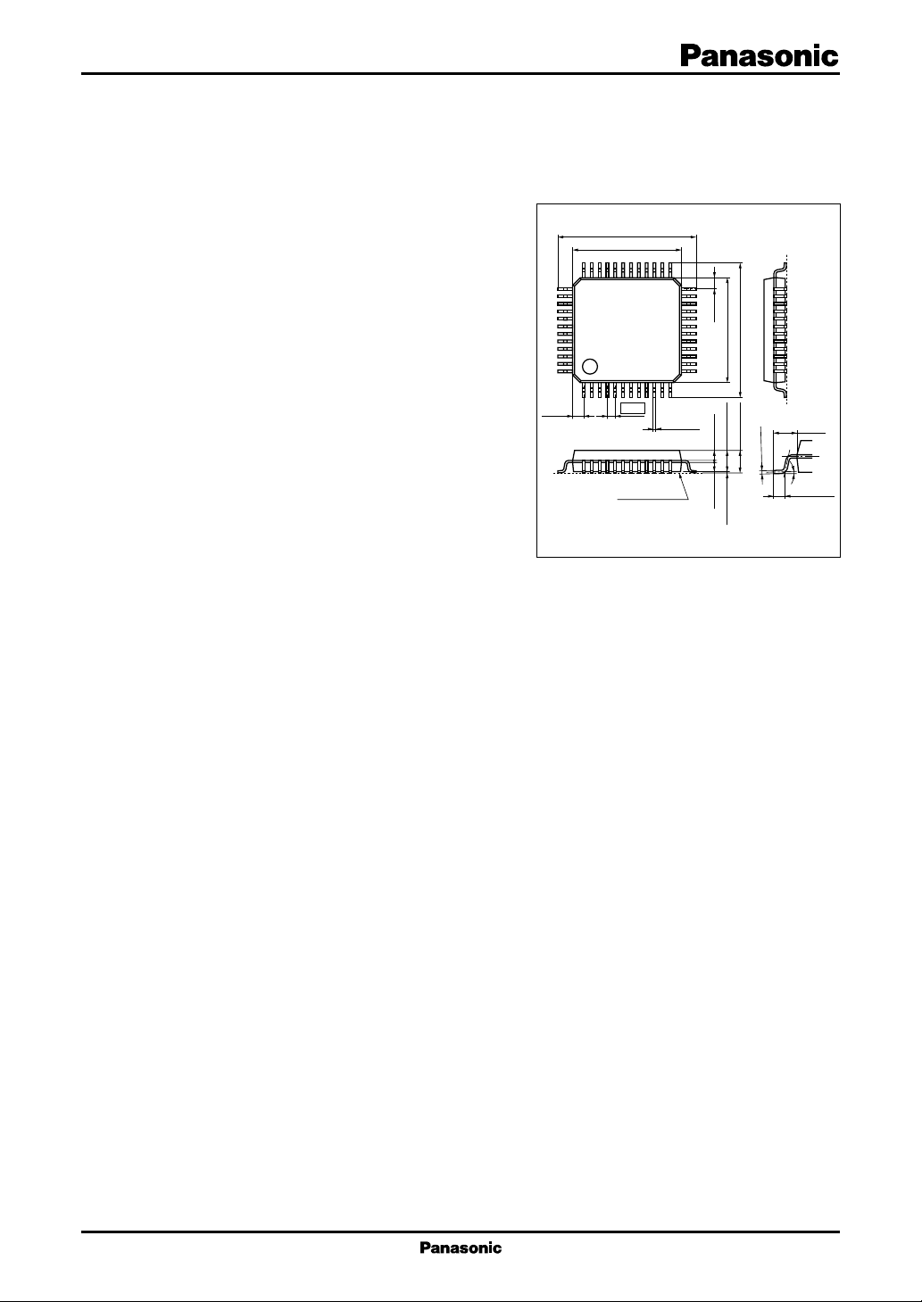
36 25
37
1
(0.75)
9.00±0.40
7.00±0.20
12
0.50
0.20
Seating plane
LQFP048-P-0707
+0.10
–0.05
24
1348
(0.75)
7.00±0.20
1.40±0.10
(0.625)(0.625)
0.10±0.10
Unit: mm
9.00±0.40
–0.05
+0.10
1.70 max.
0.15
(1.00)
0° to 10°
0.50±0.20
1
Page 2
AN7500FHQ ICs for Radio-Cassette, Cassette Deck
■ Block Diagram
REF
N.R. in (L)
36
35
I
34
N.R. out (L)
33
32
31
30
SB out (L)
29
28
PWR in (L)
27
26
PWR in (R)
25
PB out (L)
REV in (L)
FWD in (L)
V
REF
FWD in (R)
REV in (R)
PB out (R)
37
38
39
40
25 kΩ 200 kΩ
41
42
43
Bias
44
45
25 kΩ
46
200 kΩ
47
48
N.R.
FWD
REV
On Off
mute
1
160 Ω
24
86 kΩ
100 kΩ
V
REF
V
REF
23
22
21
PWR out (R)
20
V
CC
19
GND
18
PWR out (L)
17
AGC
16
Ripple
filter
V
V
REF
REF
15
14
100 kΩ
86 kΩ
Control
13
STBY
160 Ω
2
3
4
5
6
7
8
9
10
11
12
ASC
N.R. in (R)
N.R. out (R)
SB out (R)
Low BST
Power mute
2
Page 3
ICs for Radio-Cassette, Cassette Deck AN7500FHQ
■ Pin Descriptions
Pin No. Description
1 FWD/REV/pre-mute control
2 Noise reduction on/off control
3 N.R. decoder input (R)
4 N.R. decoder output (R)
5 Side-chain filter (R)
6 Weighting amp. filter (R)
7 Control voltage ripple filter (R)
8 Sub-buffer amp. output (R)
9 Sub-buffer amp. input (R)
10 Sub-buffer amp. on/off control
11 Low boost on/off control
12 Power mute on/off control
13 Standby on/off control
14 Ripple filter input
15 Ripple filter base pin
16 Ripple filter output
17 AGC time constant
18 Power output (L)
19 GND pin
20 Positive power supply
21 Power output (R)
22 Low boost capacitor pin 2
23 LPF2 capacitor pin
24 Low boost capacitor pin 1
Pin No. Description
25 Power input (R)
26 LPF1 capacitor pin
27 Power input (L)
28 Sub-buffer amp. input (L)
29 Sub-buffer amp. output (L)
30 Control voltage ripple filter (L)
31 Weighting amp. filter (L)
32 Side-chain filter (L)
33 N.R. decoder output (L)
34 N.R. decoder input (L)
35 Reference current resistance pin
36 MS LPF C pin
37 MS output
38 MS filter pin
39 Playback amp. output (L)
40 Playback amp. negative feedback input (L)
41 Playback amp. REV input (L)
42 Playback amp. FWD input (L)
43 Reference voltage output
44 Playback amp. FWD input (R)
45 Playback amp. REV input (R)
46 Playback amp. negative feedback input (R)
47 Playback amp. output (R)
48 Reference voltage input
■ Absolute Maximum Ratings
Parameter Symbol Rating Unit
Supply voltage V
Supply current I
2
Power dissipation
Operating ambient temperature
Storage temperature
Note)*1: Except for the operating ambient temperature and storage temperature, all ratings are for Ta = 25°C.
2: Ta = 75°C
*
*
1
*
1
*
CC
CC
P
D
T
opr
T
stg
2.1 V
20 mA
249 mW
−20 to +70 °C
−55 to +125 °C
3
Page 4
AN7500FHQ ICs for Radio-Cassette, Cassette Deck
■ Recommended Operating Range
Parameter Symbol Range Unit
Supply voltage V
Note)*: Supply voltage of VCC of 0.95 V to 0.98 V is permissible as long as it does not cause any abnormal operation such as oscillation.
CC
■ Electrical Characteristics at VCC = 1.2 V, f = 1 kHz, RL = 32, Ta = 25°C
Parameter Symbol Conditions Min Typ Max Unit
Voltage gain G
Circuit current 1 I
Circuit current 2 I
Circuit current 3 I
Circuit current 4 I
Circuit current 5 I
Pre-amp. block
Open-loop voltage gain G
Close-loop voltage gain G
Max. output voltage
V
omax(PB)
Total harmonic distortion THD
Output noise voltage V
Channel separation CS
FWD/REV crosstalk CT
Ripple rejection factor RR
Mute attenuation amount
G
MUTE(PB)
Heavy low sound + power amp. block
Gain voltage 1 G
Gain voltage 2 G
Low frequency boost amount G
Rated output power P
Total harmonic distortion THD
Channel separation 1 CS1
VO = −22.2 dBV 54 57 60 dB
V
VIN = 0, Rg = 2.2 kΩ, 3.2 5.9 mA
CC1
L. BST off, N.R. off
VIN = 0, Rg = 2.2 kΩ, 4.4 7.1 mA
CC2
L. BST off, N.R. on
CC3Pout
CC4Pout
= 0.5 mW × 2-ch., RL = 32 Ω7.0 11.2 mA
= 0.5 mW × 2-ch., 8.4 12.8 mA
RL = 32 Ω, N.R. on
STBY on 15 30 µA
CC5
VO(PB)VO
VC(PB)VO
= −22.2 dBV 61 73 dB
= −22.2 dBV 32.5 34 35.5 dB
THD = 1%, 30 kHz, LPF on 120 210 mV
= −22.2 dBV, 30 kHz, LPF on, 0.2 0.6 %
(PB)VO
GVC = 35 dB (NAB)
NO(PB)Rg
(PB)
= 2.2 kΩ, IHF-A −90 −76 dBV
Sincgle ch. input, 1 kHz, BPF on, 37 46 dB
Rg = 2.2 kΩ, VO = −22.2 dBV
Single ch. input, 1 kHz, BPF on, 51 59 dB
(PB)
Rg = 2.2 kΩ, VO = −22.2 dBV
(PB)Rg
= 2.2 kΩ, VRR = −32.2 dBV, 43 53 dB
f
= 100 Hz, I
RR
RFO
BPF: 100 Hz, 1/4 OCT
Ratio to VO = −22.2 dBV, −85 −70 dB
pre-mute on
V1(PW)VO
V2(PW)
V3(PW)
= −22.2 dBV 21 23 25 dB
L. boost on, VO = −22.2 dBV 21.4 23.4 25.4 dB
L. boost on/off, 15 19 23 dB
f = 50 Hz, VIN = 65.2 dBV
THD = 10%, 30 kHz, LPF on 2.5 4.5 mW
out
(PW)Pout
(PW)
= 1 mW, 30 kHz, LPF on 0.35 1.3 %
Sincgle ch. input, 1 kHz, BPF, 33 40 dB
Rg = 0, VO = −22.2 dBV
0.98 * to typ. 1.2 to 2.0 V
= 15 mA,
4
Page 5
ICs for Radio-Cassette, Cassette Deck AN7500FHQ
■ Electrical Characteristics at VCC = 1.2 V, f = 1 kHz, RL = 32, Ta = 25°C (continued)
Parameter Symbol Conditions Min Typ Max Unit
Heavy low sound + power amp. block (continued)
Channel separation 2 CS2
Output noise voltage 1
Output noise voltage 2
V
NO1(PW)Rg
V
NO2(PW)
Ripple rejection factor 1 RR1
Ripple rejection factor 2 RR2
Input resistance R
Channel balance CB
Mute output voltage
V
MUTE(PW)VIN
AGC level V
Output DC step DV
Dolby block
1
Reference input level
*
V
Channel balance CB
2
N.R. decode characteristics 1
N.R. decode characteristics 2
N.R. decode characteristics 3
N.R. decode characteristics 4
N.R. decode characteristics 5
Note)*1: Adjust an input level to get an output level of −3.2 dBV at a measuring point (N.R. out) so that you can get 0 dB of reference
input level.
2: VO in the calculating equation is the output level based on reference of 0 dB = −32.2 dBV (measuring point: N.R. out).
*
*
G
2
*
G
2
*
G
2
*
G
2
*
G
Sincgle ch. input, Low boost on, 25 31 dB
(PW)
Rg = 0, VO = −22.2 dBV, 1 kHz, BPF
= 0, IHF-A −91 −86 dBV
Low boost on, Rg = 0, IHF-A −86 −82 dBV
= 0, VRR = −32.2 dBV, 60 72 dB
(PW)Rg
fRR = 100 Hz, I
= 15 mA,
RFO
BPF: 100 Hz, 1/4 OCT
Low boost on, Rg = 0, 40 61 dB
(PW)
V
= −32.2 dBV, fRR = 100 Hz,
RR
I
= 15 mA, BPF: 100 Hz, 1/4 OCT
RFO
IN(PW)
(PW)VO
= −22.2 dBV −1.5 0 1.5 dB
7.2 9.5 12 kΩ
= −32.2 dBV −96 −90 dBV
AGCVIN
= −45.2 dBV, f = 100 Hz, −17.3 −14.7 −13.1 dBV
R
= 32 Ω,
L
AGC level to be measured at 32 Ω end.
PWR mute (pin 12) on/off −30 0 30 mV
(PW)
N.R.: Off, BEF: Off, f = 1 kHz, −33.9 −32.8 −31.7 dBV
IN(NR)
VO = −32.2 dBV
(Calculation) channel ratio of the above −10 1 dB
(NR)
V
IN
N.R.: On, BEF: Off, f = 10 kHz, −20 2 dB
(NRD1)
V
= −29.6 dB,
IN
Calculation NRD = VO +40 (dB)
N.R.: On, BEF: Off, f = 1 kHz, −20 2 dB
(NRD2)
VIN = −23.9 dB,
Calculation NRD = VO +30 (dB)
N.R.: On, BEF: Off, f = 1 kHz, −3.0 0 3.0 dB
(NRD3)
V
= −15.8 dB
IN
Calculation NRD = VO +20 (dB)
N.R.: On, BEF: Off, f = 10 kHz, −2.5 0 2.5 dB
(NRD4)
V
= −17.4 dB
IN
Calculation NRD = VO +20 (dB)
N.R.: On, BEF: Off, f = 10 kHz, −20 2 dB
(NRD5)
VIN = 0.4 dB,
Calculation NRD = VO (dB)
5
Page 6

AN7500FHQ ICs for Radio-Cassette, Cassette Deck
■ Electrical Characteristics at VCC = 1.2 V, f = 1 kHz, RL = 32, Ta = 25°C (continued)
Parameter Symbol Conditions Min Typ Max Unit
Dolby block (continued)
3
*
Total harmonic distortion 1
Total harmonic distortion 2
Total harmonic distortion 3
THD1
3
*
THD2
3
*
THD3
(Signal handling) V
4
Signal to noise ratio, N.R. on
Sub-buffer filter characteristic
*
V
5
*
G
Ripple filter block
Ripple rejection factor RR V
DC output voltage V
Bias block
DC output voltage V
AMS block
Music detection level 1 V
Music detection level 2 V
Control block
Standby-off voltage V
Standby-on voltage V
Standby pin current I
Power mute-on threshold V
Power mute-off threshold V
Power mute pin current I
FWD/REV/pre-mute low threshold
FWD/REV/pre-mute high threshold
V
V
FWD/REV/pre-mute pin current I
Low-boost on threshold V
Low-boost pin current I
N.R. on threshold V
N.R. off threshold V
Note)*3: Measuring point: SB out
4: Measuring point: N.R. out
*
5: Attenuation amount referred to sub-buffer off (measuring point: SB out).
*
N.R.: Off, BEF: On, f = 1 kHz, 0.2 0.5 %
(NR)
VIN = +10 dB, 30 kHz, LPF on
N.R.: On, BEF: Off, f = 1 kHz, 0.3 0.8 %
(NR)
VIN = +10 dB, 30 kHz, LPF on
N.R.: On, BEF: Off, f = 1 kHz, 0.3 1 %
(NR)
= +12 dB
IN
VCC = 1.1 V, 30 kHz, LPF on
N.R.: On, BEF: Off, 70 72 dB
NO(NR)
Input pin R
= 15 kΩ,
g
CCIR/ARM filter
N.R.: Off, BEF: On/off, f = 6.3 kHz, −12 −8dB
VOP2
VIN = 0 dB
= 1.1 V, VRR = −32.2 dBV 24 30 dB
CC
f
= 100 Hz, I
RR
= 15 mA
RFO
BPF: 100 Hz, 1/4 OCT
RPFVCC
REFVCC
BS
MS
STOFF
STON
STBYV13
MTON
MTOFF
SW12V12
TH1L
TH1H
SW1V1
LBON
SW11V11
NRON
NROFF
= 1.0 V, I
= 1.0 V 0.68 0.76 0.83 V
Power mute on, at V37 = 0.6 V[p-0] −50.6 −49 −47.4 dBV
Power mute off, at V37 = 0.6 V[p-0] −66.6 −65 −63.4 dBV
Low: Power on 0.4 V
High/open: Power off 0.75 V
= 0 V 16 45 µA
Low: Power mute on 0.3 V
High/open: Power mute off 1.05 V
= 0.1 V 20 40 µA
Low: REV 0.1 V
High: Pre-mute on 1.1 V
= 0.1 V 918µA
Low: Low boost on 0.3 V
= 0.1 V 20 40 µA
Low: N.R. on 0.4 V
High/open : N.R. off 0.8 V
= 15 mA 0.89 0.94 V
RFO
6
Page 7

ICs for Radio-Cassette, Cassette Deck AN7500FHQ
■ Electrical Characteristics at VCC = 1.2 V, f = 1 kHz, RL = 32, Ta = 25°C (continued)
Parameter Symbol Conditions Min Typ Max Unit
Control block (continued)
N.R. pin current I
Sub-buffer on threshold V
Sub-buffer off threshold V
Sub-buffer pin current I
■ Terminal Equivalent Circuits
V2 = 0.1 V 816µA
SW2
Low: SB on 0.4 V
SBON
High/open: SB off 0.8 V
SBOFF
SW10V10
= 0.1 V 20 40 µA
Pin No. Equivalent circuit Description
1 FWD/REV/pre-mute:
120 kΩ
1
V
RPF
FWD/REV/pre-mute control
Pre-mute
High voltage: V
CC− 0.1
< V
1-19
Waveform/voltage
(at VCC = 1.2 V)
FWD
Pin open
120 kΩ
REV
Low voltage: V
1-19
< 0.1
GND
2 N.R. cont.: RIN = 33 kΩ
Approx.
2 µA
2
200 Ω
100kΩ100
100 kΩ
kΩ
V
RPF
N.R. on/off control 0.8 V
N.R. off
Pin open or high voltage:
0.8 V < V
< VCC +0.3 V
2-19
N.R. on
Low voltage:
− 0.3 V < V
2-19
< 0.4 V
GND
3 Pin 3: N.R. in (R)
V
34 Pin 34: N.R. in (L):
RPF
V
REF
N.R. decoder input
Pin 3
34
30 kΩ
= 30 kΩ (typ.)
R
IN
50 kΩ
DC 0.78 V
GND
7
Page 8

AN7500FHQ ICs for Radio-Cassette, Cassette Deck
■ Terminal Equivalent Circuits (continued)
Pin No. Equivalent circuit Description
4 Pin 4: N.R. out (R) R
V
33 Pin 33: N.R. out (L): DC 0.78 V
V
REF
RPF
N.R. decoder output
Waveform/voltage
(at VCC = 1.2 V)
= 300 Ω (typ.)
O
6.7 kΩ
Pin 4
33
11.6 kΩ
7.5 kΩ
GND
5 Pin 5: SC in (R) RIN:
V
32 Pin 32: SC in (L): to inpuit signal
V
REF
Pin 5
32
200
Ω
EVR
RPF
Side chain input DC 0.78 V
Variable according
GND
6 Pin 6: WAMP (R) DC 0.78 V
V
31 Pin 31: WAMP (L):
Pin 6
31
V
REF
270 Ω
RPF
Weighting amp. filter pin
GND
7 Pin 7: VC LPF (R) 0 V
30 Pin 30: VC LPF (L): (Add external resistor
V
RPF
Control voltage ripple filter pin without signal)
Pin 7
30
GND
8
Page 9

ICs for Radio-Cassette, Cassette Deck AN7500FHQ
■ Terminal Equivalent Circuits (continued)
Pin No. Equivalent circuit Description
8 Pin 8: SB out (R) At SB on
29 Pin 29: SB out (L): R
V
REF
100 kΩ
Pin 8
29
160 Ω
V
RPF
Sub-buffer amp. output At SB off
When pin 10 is open or of high R
voltage and output is connected to DC 0.78 V
V
with 100 kΩ, the buffer amp.
REF
Waveform/voltage
(at VCC = 1.2 V)
= 160 Ω (typ.)
O
= 100 kΩ (typ.)
IN
does not operate.
GND
9 Pin 9: SB in (R) RIN = 86 kΩ (typ.)
28 Pin 28: SB in (L): DC 0.78 V
V
REF
V
RPF
Sub-buffer amp. input
86
kΩ
Pin 9
28
GND
10 SB CNT: RIN = 6 kΩ
50 kΩ
V
RPF
Sub-buffer amp. on/off control DC 0.78 V
SB off
Pin open or high voltage:
10
20 kΩ
20 kΩ
20 kΩ
0.8 V < V
SB on
Low voltage:
− 0.3 V < V
< VCC +0.3 V
10-19
< 0.4 V
10-19
GND
11 L-BST CNT: DC 0 V
V
RPF
Low boost on/off control
11
50 kΩ
10 kΩ
50 kΩ
L-BST on
Pin open
L-BST off
Low voltage:
− 0.3 V < V
10-19
< 0.3 V
GND
9
Page 10

AN7500FHQ ICs for Radio-Cassette, Cassette Deck
■ Terminal Equivalent Circuits (continued)
Pin No. Equivalent circuit Description
12 PWR mute CNT: DC 0 V
V
RPF
Power mute on/off control
12
50 kΩ
PWR-mute off
Pin open or high voltage:
VCC − 0.15 V < V
12-19
< VCC +0.3 V
PWR-mute on
50 kΩ
Low voltage:
− 0.3 V < V
12-19
< 0.3 V
GND
13 STBY CNT: DC 0 V
V
RPF
Standby on/off control
STBY off
100
kΩ
13
Pin open or high voltage:
0.75 V < V
< VCC +0.3 V
13-19
STBY (on state) on
100 kΩ
Low voltage:
− 0.3 V < V
13-19
< 0.4 V
GND
Waveform/voltage
(at VCC = 1.2 V)
14 RF in: DC 1.0 V
70 kΩ
14
V
CC
Ripple filter reference voltage input
14 kΩ
15 RF base: DC 0.47 V
350 kΩ
100 kΩ
Ripple filter
GND
16 V
15
: DC 1.13 V
RPF
Ripple filter reference voltage output
16
10
Page 11

ICs for Radio-Cassette, Cassette Deck AN7500FHQ
■ Terminal Equivalent Circuits (continued)
Pin No. Equivalent circuit Description
17 AGC TAU:
17
V
RPF
AGC time constant
Waveform/voltage
(at VCC = 1.2 V)
GND
18 Pin 18: PWR out (L)
21 Pin 21: PWR out (R):
60 kΩ
Pin 18
21
4 kΩ
V
CC
Power amp. voltage output
DC 0.6 V
GND
19 GND pin 0 V
20 VCC power supply pin 1.2 V
22 L-BST C:
15 kΩ
V
RPF
Low boost capacitor pin
7.5 kΩ
22
7.5 kΩ
V
REF
15 kΩ
GND
23 LPF2-C:
45 kΩ
V
RPF
LPF2 capacitor pin
15 kΩ
23
7.5
kΩ
V
REF
GND
DC 0.78 V
DC 0.78 V
11
Page 12

AN7500FHQ ICs for Radio-Cassette, Cassette Deck
■ Terminal Equivalent Circuits (continued)
Pin No. Equivalent circuit Description
24 L-BST C1:
3 kΩ
24
30
kΩ
V
REF
30 kΩ
3 kΩ
V
RPF
Low boost capacitor pin
GND
25 Pin 25: PWR in (R)
V
27 Pin 27: PWR in (L):
RPF
Power amp. input
2 kΩ
12 kΩ
V
REF
GND
LPF capacitor pin
25
90 kΩ
10 kΩ
V
REF
V
RPF
26 LPF1-C:
90 kΩ
27
10 kΩ
Waveform/voltage
(at VCC = 1.2 V)
DC 0.78 V
DC 0.78 V
AC −30 dBm
GND
V
RPF
26
GND
35 I
35
V
GND
12
: DC 0.1 V
RPF
REF
Reference current resistor pin
DC 0.78 V
Page 13

ICs for Radio-Cassette, Cassette Deck AN7500FHQ
■ Terminal Equivalent Circuits (continued)
Pin No. Equivalent circuit Description
Waveform/voltage
(at VCC = 1.2 V)
36 MS LPF-C:
V
RPF
Music interval detection LPF capa-
10 kΩ
36
citor pin
5.7 kΩ
GND
37 MS out:
V
CC
37
Music interval detection output
400 kΩ
GND
38 MS-C: DC 0.78 V
V
RPF
Music interval detection filter capa-
180 kΩ
citor pin
180 kΩ
38
180 kΩ
V
REF
180 kΩ
GND
13
Page 14

AN7500FHQ ICs for Radio-Cassette, Cassette Deck
■ Terminal Equivalent Circuits (continued)
Pin No. Equivalent circuit Description
39 Pin 39: PB out (L)
47 Pin 47: PB out (R):
V
CC
Playback amp. output
Pin 39
47
GND
40 Pin 40: PB NF (L)
46 Pin 46: PB NF (R):
V
CC
Playback amp. negative feedback
input
Pin 40
46
GND
41 Pin 41: REV in (L)
45 Pin 45: REV in (R):
Playback amp. REV input
Waveform/voltage
(at VCC = 1.2 V)
DC 0.6 V
AC −30 dBm
DC 0.78 V
1 kHz −65 dBm
V
CC
42 Pin 42: FWD in (L)
44 Pin 44: FWD in (R):
Playback amp. FWD input
Pin 41
42
44
45
V
25 kΩ
REF
200 kΩ
GND
14
DC 0.78 V
AC −65 dBm
Page 15

ICs for Radio-Cassette, Cassette Deck AN7500FHQ
■ Terminal Equivalent Circuits (continued)
Pin No. Equivalent circuit Description
43 V
V
RPF
43
: DC 0.78 V
REF
Reference voltage output
GND
48 V
V
RPF
48
in: DC 0.78 V
REF
Reference voltage input
GND
Waveform/voltage
(at VCC = 1.2 V)
15
Page 16

AN7500FHQ ICs for Radio-Cassette, Cassette Deck
■ Application Circuit Example
PB out (L)
0.022 µF
180 Ω
REV in (L)
FWD in (L)
V
REF
FWD in (R)
REV in (R)
180 Ω
0.022 µF
PB out (R)
0.047 µF
33 µF
22 µF
33 µF
1 µF
6.8
kΩ
1 µF
1 µF
1 µF
1 µF
6.8
kΩ
1 µF
2.2 µF
36
37
38
39
40
25 kΩ 200 kΩ
41
42
43
Bias
44
45
25 kΩ
46
200 kΩ
47
48
N.R.
FWD
REV
On Off
mute
1
N.R. in (L)
N.R. out (L)
0.33 µF
REF
I
3 300 pF
1 µF
10 kΩ
35
34
33
1 µF
0.01 µF
32
31
390 kΩ
15 kΩ
2 700 pF
30
29
160 Ω
2.2 kΩ
0.01
µF
PWR in (L)
SB out (L)
28
PWR in (R)
1 µF
27
1 µF
0.1 µF
26
25
6.8 µF
24
86 kΩ
0.15 µF
Ripple
filter
23
22
21
20
19
18
17
16
15
14
6.8 µF
0.1 µF
100 µF
100 µF
0.1 µF
0.047 µF
33 µF
2.2 Ω
PWR out (R)
GND
PWR out (L)
2.2 Ω
22 µF
2SB1295
32 Ω
V
32 Ω
CC
100 kΩ
V
REF
V
REF
AGC
V
V
REF
REF
100 kΩ
On
Off
STBY
86 kΩ
Control
13
160 Ω
2
3
4
5
6
7
8
9
10
11
12
Mute
V
CC
FWD
REV
Off
On
1 µF
1 µF
N.R. in (R)
N.R. out (R)
3 300 pF
15 kΩ
0.01 µF
0.33 µF
1 µF
2 700 pF
0.01 µF
390 kΩ
2.2 kΩ
SB out (R)
Off
On
On
ASC
Note) Dolby and double D logos are the trademarks of Dolby Laboratories Licensing Corporation.
The use of this product requires the prior approval of Dolby Laboratories Licensing Corporation.
16
Off
Low BST
Off
On
Power mute
 Loading...