

Page 1
ICs for FM/AM Tuner
AN7298FBP
FM-IF, NC, and MPX IC for car radio
■ Overview
The AN7298FBP is an IC for car radio. The FM-IF,
NC (Noise Canceler) and MPX functions are integrated
into a single chip. The IC has the higher functions than
our conventional IC (AN7292NSC) and the characteristics of multi-pass detection, mute and SD functions are
improved.
■ Features
• IF sensitivity is high. (limiting sensitivity 26 dBµ)
• Adjustment-free VCO (912 kHz)
• Good linearity of S-meter output (adjusting funciton)
■ Applications
• Car radios
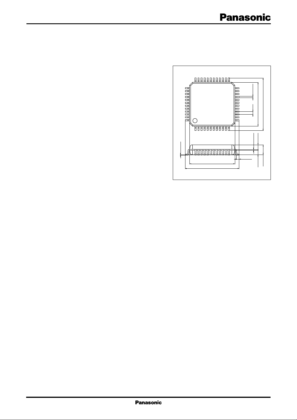
36 25
37
48
1
0.1±0.1
12
12.0±0.3
14.2±0.4
QFH048-P-1212
Unit: mm
24
13
(0.55)
+0.10
0.3±0.10.8
–0.05
0.15
14.2±0.4
12.0±0.3
1.3±0.1
2.8±0.2
1.3±0.1
1
Page 2
AN7298FBP ICs for FM/AM Tuner
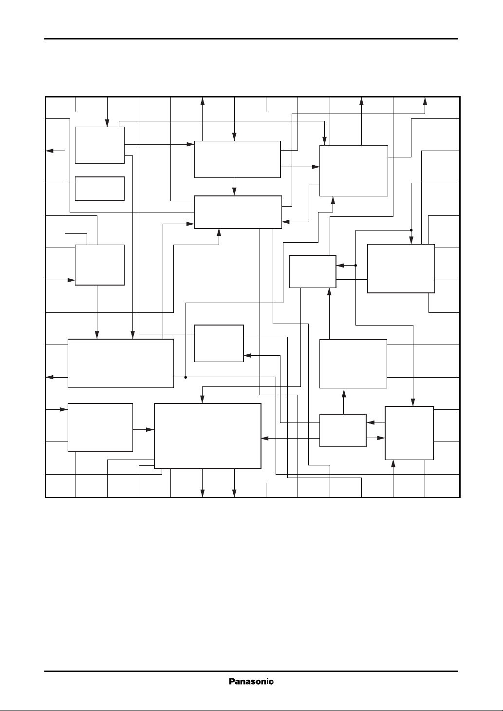
■ Block Diagram
37
38
39
40
41
42
43
44
45
GND
36
2nd
limiter
Reg.
1st
limiter
V
V
cont
35
det.
cont
DC amp.
34
33
32
Pilot
31
Quad det.
AFC amp.
Mute amp.
det.
30
V
CC
29
PNL
28
Band det.
IF count.
canceler
SD
Pilot
27
26
Pulse det.
AGC
25
24
23
22
21
20
19
18
17
16
46
47
48
Multipath
detector
1
ASC .ATC
stereo
demod.
2
3
4
5
6
7
8
Divider
9
10
VCO
11
15
14
13
12
2
Page 3

ICs for FM/AM Tuner AN7298FBP
■ Pin Descriptions
Pin No. Description
1 ASC adjustment
2 ATC adjustment
3 Separation adjustment
4 ATC LPF
5 R-ch. output
6 L-ch. output
7 Control voltage output
8 Band mute control
9 Soft mute filter
10 Phase detection filter1
11 Forced monaural
12 Phase detection filter 2-1
13 SD startup time constant setting
14 Phase detection filter 2-2
15 VCO
16 Phase detection filter 3
17 Pilot canceler negation filter
18 PNL LPF
19 PNL LPF
20 PNL gate pulse filter
21 PNL AGC
22 PNL input
23 PNL HPF
24 IF-counter output stop
Pin No. Description
25 IF detection output
26 PNL output hold
27 SD/IF counter output
28 SD sensitivity adjustment
29 AFC output
30 V
CC
31 IF detection coil
32 Limiter output
33 Soft mute adjustment
34 Stereo lamp drive
35 2nd limiter output
36 GND
37 Mute adjustment
38 1st limiter
39 Reference voltage
40 1st limiter output GND
41 1st limiter bias
42 IF input
43 Mute slope adjustment
44 Control voltage adjustment
45 Control voltage output
46 Control voltage input
47 ASC
48 Control voltage detection
■ Absolute Maximum Ratings
Parameter Symbol Rating Unit
Supply voltage V
Supply current I
2
Power dissipation
Operating ambient temperature
Storage temperature
Note)*1 : All parameter values except for the power dissipation, the operating ambient temperature and the storage temperature are
Ta = 25°C.
*2 : Power dissipation of IC alone at Ta = 80°C.
*
1
*
1
*
CC
CC
P
D
T
opr
T
stg
9.7 V
48 mA
301 mW
−30 to +80 °C
−55 to +125 °C
3
Page 4

AN7298FBP ICs for FM/AM Tuner
■ Recommended Operating Range
Parameter Symbol Range Unit
Supply voltage V
CC
7.2 to 9.6 V
■ Electrical Characteristics at VCC = 8 V, fIN = 10.70 MHz, f
= 1 kHz 30%FM, Ta = 25°C
mod
Parameter Symbol Conditions Min Typ Max Unit
Control voltage 1 V
Control voltage 2 V
Control voltage 3 V
Control voltage 4 V
Control voltage 5 V
Control voltage 6 V
AFC offset voltage V
Without input, pin 45 DC voltage 0.05 0.50 0.90 V
C1
VIN = 40 dBµ, pin 45 DC voltage 1.20 1.65 2.10 V
C2
VIN = 70 dBµ, pin 45 DC voltage 2.75 3.45 4.15 V
C3
VIN =100 dBµ, pin 45 DC voltage 4.45 5.35 6.25 V
C4
VC5 = VC3−V
C5
VC6 = VC4−V
C6
Without input, DC voltage between
AFC
C2
C3
1.60 1.80 2.00 V
1.70 1.90 2.10 V
− 0.1 0.0 0.1 V
pin 29 and pin 39
Output level L V
Output level R V
VIN = 70dBµ, pin 6 AC voltage 90 110 130
OL
VIN = 70dBµ, pin 5 AC voltage 90 110 130
OR
mV[rms]
mV[rms]
Channel balance CB CB = 20Log (VOL /VOR) −1.0 0.0 1.0 dB
Limiting sensitivity V
VOL to 0 dB. Input when pin 6 20.0 26 30.0 dBµ
lim
AC voltage drops by 3 dB
Residual pilot voltage V
Pin 26 output when VIN = 70 dBµ, 4 14.0
PC
mV[rms]
pilot signal 10% modulation
Stereo lamp on-level Lamp
Modulation with pilot signal only, 1.0 3.5 6.0 %
ON
DC voltage of pin 34 is below 2 V
Stereo lamp off-level Lamp
Modulation with pilot signal only. 2.0 6.0 10.0 dB
OFF
Ratio of stereo lamp on and off
level
Separation L-ch. Sep
VIN = 70 dBµ, L+R = 90% 25 33 dB
L
Pilot 10%
Separation R-ch. Sep
VIN = 70 dBµ, L+R = 90% 25 33 dB
R
Pilot 10%
Capture range CR V
= 70 dBµ, +0.6 +0.8 %
IN
pilot signal 6.5% modulation −0.2 0.4
Counter output level 1 V
IF1
V
= 70 dBµ, pin 28 = 0V, 0 2.0 5.0
IN
mV[rms]
pin 27 10.7 MHz, output voltage
Counter output level 2 V
IF2
= 70 dBµ, pin 28 = VCC, 85 100 115
IN
mV[rms]
V
pin 27 AC output voltage
Power supply current I
Monaural THD (L-ch.) THD
Without input, pin 11 = 0 V 28.0 35.0 42.0 mA
tot
Monaural input 400 mV, 1kHz, 0.15 0.3 %
L
L-ch. distortion
Monaural THD (R-ch.) THD
Monaural input 400 mV, 1kHz, 0.15 0.3 %
R
R-ch. distortion
4
Page 5

ICs for FM/AM Tuner AN7298FBP
■ Electrical Characteristics at VCC = 8 V, fIN = 10.70 MHz, f
= 1 kHz 30%FM, Ta = 25°C (continued)
mod
Parameter Symbol Conditions Min Typ Max Unit
Stereo THD (L-ch.) THD
Stereo, L+R = 360 mV,VP = 40 mV,
SL
0.15 0.3 %
L-ch. distortion
Stereo THD (R-ch.) THD
Stereo, L+R = 360 mV,VP = 40 mV,
SR
0.15 0.3 %
R-ch. distortion
AGC voltage 1 V
AGC1
Input = 0, RS = 600 Ω, 0.0 0.4 V
pin 21 DC voltage
AGC voltage 2 V
AGC2
Input V
= 2 mV[rms], 1.3 1.48 1.65 V
IN2
150 kHz, pin 21 DS voltage
V
Noise detection voltage V
DET
= 100 mV[rms],150 kHz, 0.0 0.3 V
IN2
pin 20 DC voltage
Gate pulse width PW V
Residual noise voltage V
NR
= 0.3 V[p-p], tW=1 µs, 19 24 29 µs
IN2
f=1 kHz,
pin 26 output pulse width
V
=1 V[p-p], tW =10 µs, f=1 kHz,
IN2
0.0 1.2
mV[rms]
input through LPF, L-ch. output
SD bandwidth SDW Bandwidth when SD output (pin 110 140 170 kHz
27) is over 4.5 V, V
= 2.7 V
28
SD sensitivity SDS Input when SD output (pin 27) is 45 55 65 dBµ
over 4.5 V, V
= 2.7 V
28
5
Page 6

AN7298FBP ICs for FM/AM Tuner
■ Application Circuit Example
(8 V)
CC
37
38
36
GND
35
34
33
V
32
31
30
AFC output
29
28
SD output
Counter output
27
26
25
VAF
(IF detection output)
24
23
IF counter
stop
V
ref
IF input
50 Ω
V
cont
39
40
41
42
43
44
45
46
47
48
22
21
20
19
18
17
16
15
14
13
1
2
3
4
5
6
7
8
9
10
11
12
Monaural
Stereo
2
1
Forced monaural
R out
L out
On
Off
Band mute
6
 Loading...