

Page 1
ICs for Audio Common Use
AN7164
30 W BTL audio power amplifier
■ Overview
The AN7164 is an integrated circuit designed for 30
W (V
= 21 V, 8 Ω) output power amplifier. High power
CC
output (BTL 30 W), low distortion and low noise are realized. High reliability is obtained due to various kinds
of protectors built in. Furthermore, on-off of output is
possible from standby terminal.
■ Features
• High power output
• Low distortion, Low noise
• Low shock noise when power supply is turned-on, off
• Built-in standby function
• Built-in protection circuits
(Temperature, Overcurrent, Load short circuit, Output GND short circuit)
■ Applications
• Stereo, Karaoke, TV
■ Block Diagram
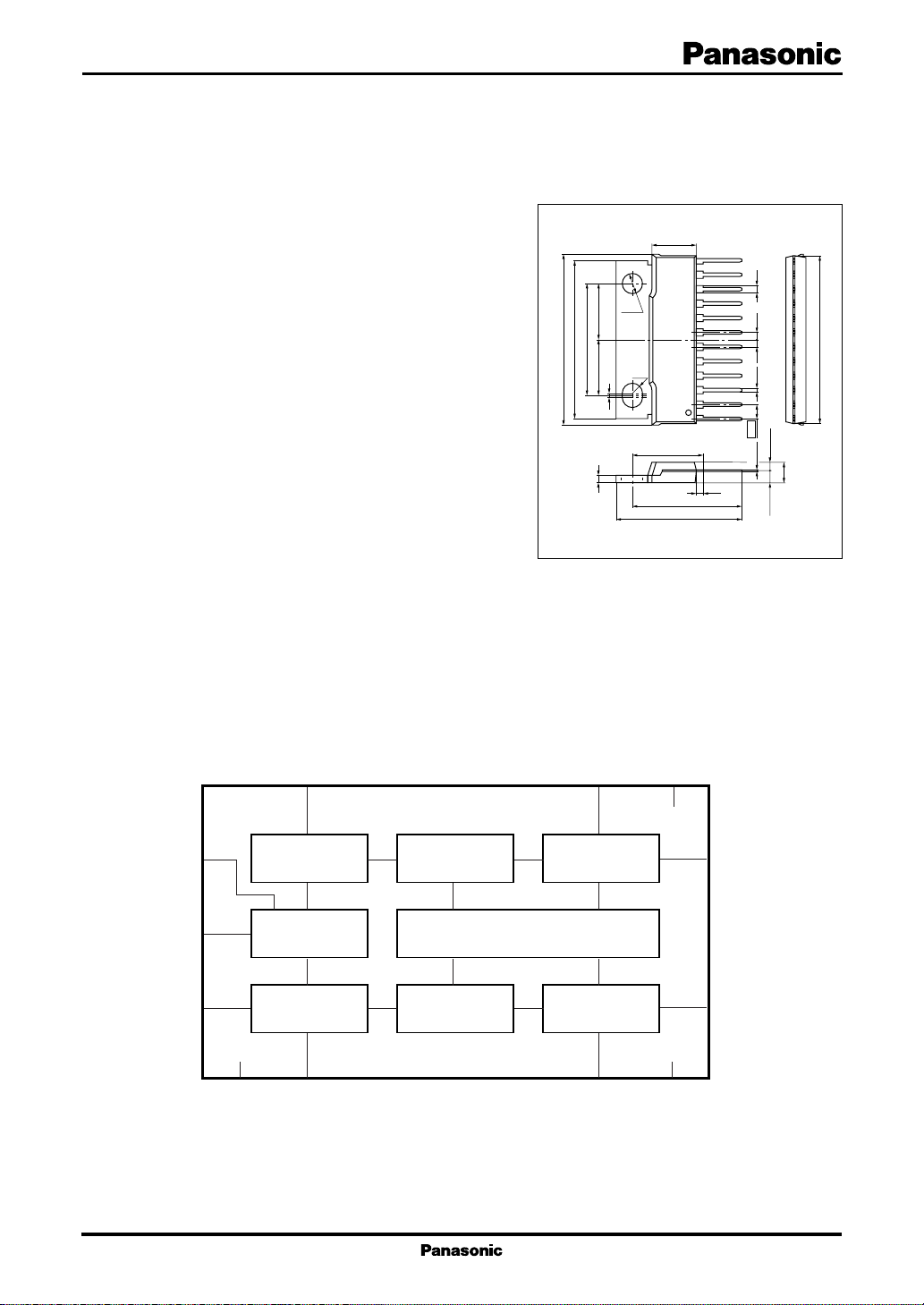
28.0±0.3
29.75±0.30
(10.0)(10.0)
20.0±0.3
1.2±0.1
φ3.6
R1.8
0.6
7.7±0.3
(12.5)
(1.2)
19.1±0.3
21.9±0.3
HSIP012-P-0000A
Unit : mm
121
(1.27) (1.3)
(1.27)
+0.15
–0.05
0.6
2.54
+0.10
–0.05
1.45±0.151.80±0.15
0.25
29.6±0.3
3.5±0.3
CC
V
12
6
1
5
3
Input circuit
Ripple filter
Input circuit
4 2
Driver circuit
Protection circuits for Temp. Overcurrent,
Load short, Output-GND short
Driver circuit
SEPP
output circuit
SEPP
output circuit
8 11
GND
10
7
9
GND
1
Page 2
AN7164 ICs for Audio Common Use
■ Pin Descriptions
Pin No. Description
1 Ripple filter
2 Negative feedback (ch.2)
3 GND (Input side)
4 Negative feedback (ch.1)
5 Input
6 Standby
■ Absolute Maximum Ratings
Parameter Symbol Rating Unit
2
Supply voltage
Supply current I
Power dissipation
Operating ambient temperature
Storage temperature
Note)*1: Ta = 25°C except power dessipation, operating ambient temperature and storage temperature.
2 : Without signal
*
3: θ
*
*
*
= 2.0 (°C/W)
j-c
V
CC
CC
3
1
*
1
*
P
D
T
opr
T
stg
Pin No. Description
7 Output (ch.1)
8 Bootstrap (ch.1)
9 GND (output side)
10 Output (ch.2)
11 Bootstrap (ch.2)
12 Supply voltage (VCC)
30 V
5.0 A
62.5 W
−30 to +75 °C
−55 to +150 °C
■ Recommended Operating Range
Parameter Symbol Range Unit
Supply voltage V
CC
8.3 to 24 V
■ Electrical Characteristics at VCC = 21 V, RL = 8 Ω, f = 1 kHz, BTL operation, Ta = 25°C
Parameter Symbol Conditions Min Typ Max Unit
Quiescent current I
Output noise voltage
Output offset voltage V
*1
V
OFF SETVIN
Total harmonic distortion THD PO = 1 W 0.07 0.3 %
Voltage gain G
Maximum output power P
Ripple rejection ratio
*1, 2
R.R. Rg = 0 Ω, power supply ripple 45 5 1 dB
Standby current I
Note)*1 : Measurement through the DIN audio filter.
2 : Power supply ripple ······ 120 Hz Sine wave, 1V[rms]
*
V
CQ
NO
= 0 V 55 100 mA
IN
Rg = 10 kΩ0.85 1.3 mV
= 0 V 0 300 mV
PO = 1 W 49.5 51.5 53.5 dB
V
THD = 10% 24 30 W
O
Pin 6 open 3 µA
STB
2
Page 3
ICs for Audio Common Use AN7164
■ Usage Notes
Standby-on (i.e. an application of 5 V to pin 6) under a high temperature may cause no-output due to the malfunction
of rapid discharging circuit of the ripple filter. To avoid this, it is necessary to forcibly flow a current of 1 mA into pin 1
at standby-on.
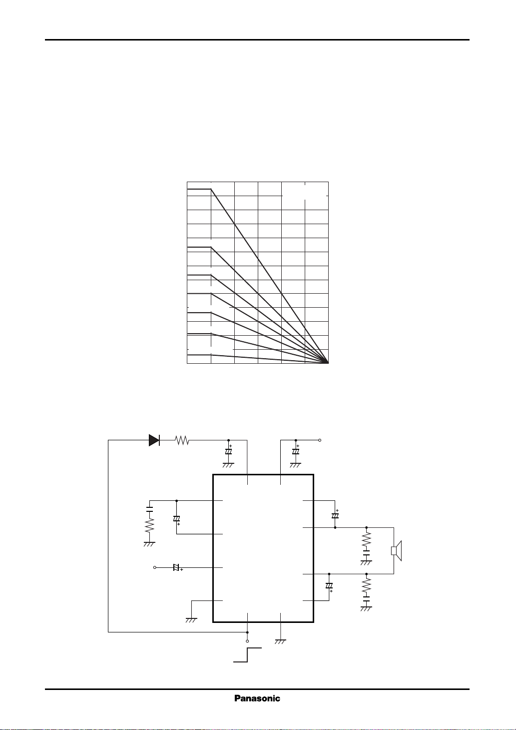
■ Technical Information
• PD Ta curves of HSIP012-P-0000A
P
T
D
65
Infinite heat sink
62.5
60
55
50
45
1°C/W heat sink
(W)
41.7
D
40
35
2°C/W heat sink
31.3
30
3°C/W heat sink
25
20
Power dissipation P
5°C/W heat sink
17.9
15
10°C/W heat sink
10.4
10
5
Without heat sink
3.0
0
0 25 50 75 100 125 150
Ambient temperature Ta (°C)
a
= 2°C/W
R
th (j−c)
= 42°C/W
R
th (j−a)
■ Application Circuit Example
0.047 µF
220 Ω
1 µF
V
IN
2 kΩ
100 µF
100 µF
V
= 21 V
CC
1 000 µF
1
2
4
12
11
10
100 µF
2.2 Ω
5
3
6
5V
0V
7
8
100 µF
2.2 Ω
0.1 µF
9
0.1 µF
8 Ω
3
 Loading...