

Page 1
AN6915, AN6916, AN6916S
Large Sink Current Dual Comparators
■ Overview
The AN6915, the AN6916 and the AN6916S are dual
voltage comparators with large output sink current and
wide range of operating supply voltage.
■ Features
• Large sink current (70mA), direct drive for relays or
lamps
• Wide range of supply voltage:VCC (opr.)=2 to 36V
• Wide range common-mode input voltage
:0 to VCC–1.5V
• Open collector output
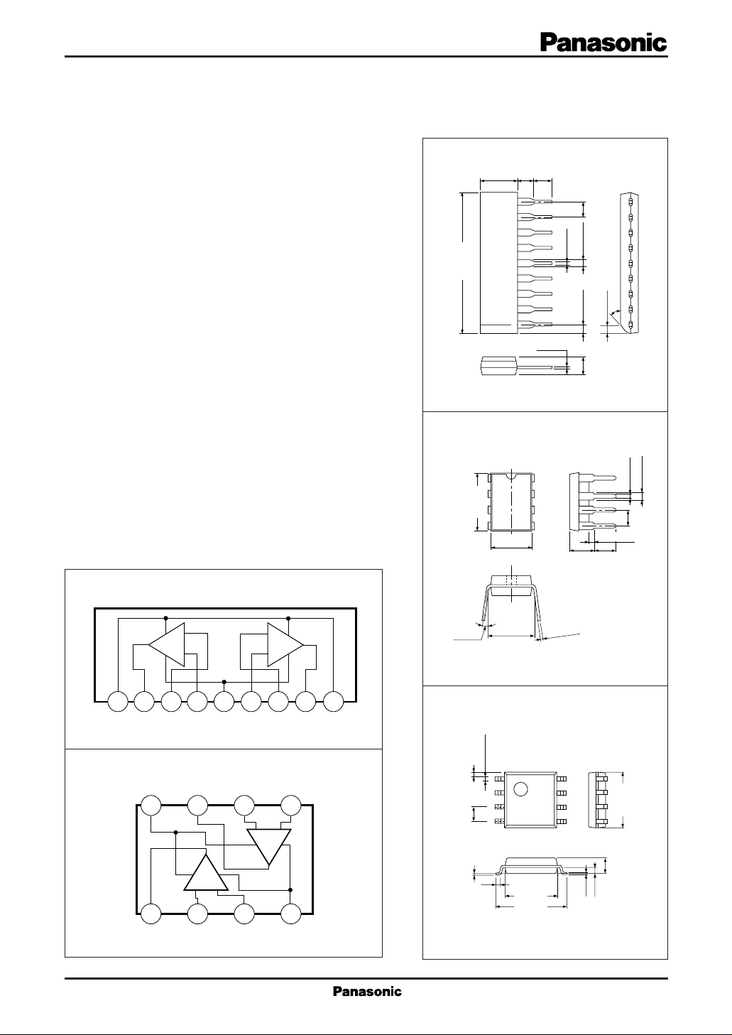
AN6916
2.4±0.25
6.0±0.3
23.3±0.3
9-pin SIL Plastic Package (SIP009-P-0000C)
3.3±0.25
9
8
7
6
5
4
3
2
1
0.3
+0.1
– 0.05
2.54
1.5±0.25
0.5±0.1
1.5±0.25
3.0±0.3
Unit:mmAN6915
30˚
1.4±0.3
Unit:mm
■ Block Diagram
AN6915
Ch.1 Ch.2
1
23456 879
V
V
CC
AN6916,AN6916S
V
O1
V
CC
8
1234
V
O1
–
+
+
–
(GND)
V
in1
in1
V
O2
–
+
+
V
V
in2
–
V
in2
765
–
Ch.2
Ch.1
+
–
–
V
in1
+
V
in1
–
in2
V
in2
+
GND
1
2
3
9.4±0.3
4
3—15˚
8-pin DIL Plastic Package (DIP008-P-0300B)
V
V
CC
O2
0.4±0.25
1
+
0.6±0.31.27
2
3
4
0.1±0.1
0.3
8-pin PANAFLAT Plastic Package (SOP008-P-0225A)
±0.3
6.3
7.62±0.25
4.2±0.3
6.5±0.3
8
7
6
5
3.8±0.25
+0.1
– 0.05
0.15
8
7
6
5
0.15
0.51min.
(3.45)
0.65
0.5±0.1
1.2±0.25
2.54
Unit:mmAN6916S
5.0±0.3
1.5±0.2
Page 2
■ Pin Descriptions
〈AN6915〉
Pin No.
1
2
3
4
5
6
7
8
9
Pin name
V
CC
Ch.1 output
Ch.1 inverting input
Ch.1 non inverting input
GND
Ch.2 non inverting input
Ch.2 inverting input
Ch.2 output
V
CC
〈AN6916, AN6916S〉
Pin No.
1
Ch.1 output
2
Ch.1 inverting input
3
Ch.1 non inverting input
4
GND
5
Ch.2 non inverting input
6
Ch.2 inverting input
7
Ch.2 output
8
V
CC
Pin name
■ Absolute Maximum Ratings (Ta=25˚C)
Parameter Symbol Rating Unit
V
VID
V
ICM
IOL
T
CC
1
*
2
*
3
*
P
D
opr
T
stg
Supply voltage
Common-mode input voltage
Differential input voltage
Output current
Power dissipation
AN6915, AN6916
AN6916S
Operating ambient temperature
Storage
temperature
*
1 The common mode input voltage is a voltage applied to the non-inverting input pin and inverting input pin simultaneously.
*
2 Differential input is equivalent to the potential difference between the non-inverting input pin and inverting input pin.
*
3 In case output level is “L”.
AN6915, AN6916
AN6916S
36
– 0.3 to +36
36
150
500
360
–30 to +85
–55 to +150
–55 to +125
V
V
V
mA
mW
˚C
˚C
■ Electrical Characteristics (VCC=5V, Ta=25˚C)
Parameter Symbol Condition min typ max Unit
Input offset voltage
Input offset current
Input bias current
Voltage gain
Common-mode input voltage range
Supply current
Response time (1)
Response time (2)
Low level output voltage
Output leakage current
V
I (offset)
I
t
t
V
I
O (Leak)
G
I
I
Bias
PLH
PHL
IO
=15kΩ
R
V
CM
CC
L
R
=∞
L
RL=5.1kΩ
=5.1kΩ
R
L
V
OL
REF
V
REF
= 0V, VI=1V, I
SINK
=70mA
=1V, VI= 0V, VO=5V
5mV1
50 nA
1
200 nA
50
200
0V
VCC–1.5
V/mV
V
5.3 mA3.8
µs2
µs1
0.4 V0.14
0.1
µA
Page 3

■ Characteristics Curve
I
10
8
(mA)
CC
6
4
Supply Current I
2
0
01020
CC –VCC
Ta=–30˚C
Ta=25˚C
Ta=85˚C
Supply Voltage VCC (V)
VOL–Ta
0.24
0.20
(V)
0.16
OL
0.12
0.08
Output Voltage V
0.04
0
–60
Ambient Temperature Ta (˚C)
–40
–20
0
20
30 40
=5V
V
CC
=70mA
I
SINK
60 100
40 80
I
100
80
(nA)
Bias
60
40
20
Input Bias Current I
0
01020
Bias–VCC
Ta=–30˚C
Ta=25˚C
Ta=85˚C
Supply Voltage V
Transfer Characteristics (1)
6
(V)
O
V
=5V
CC
5
4
80mV
3
2
1
(mV) Output Voltage V
0
I
100
50
0
Input Voltage V
0123456
Time t
Overdrive
5mV
20mV
50mV
(µs)
PLH
30 40
(V)
CC
VOL–I
1.6
1.4
(V)
O
1.2
1.0
0.8
0.6
0.4
Low-Level Output Voltage V
0.2
0
0 40 80 120 160 200
SINK
Ta=85˚C
Ta=–30˚C
Output Sink Current I
Transfer Characteristics (2)
6
(V)
O
5
4
3
2
80mV
1
(mV) Output Voltage V
0
I
0
–50
–100
Input Voltage V
0123456
Time t
20mV
50mV
5mV
PLH
Overdrive
(µs)
Ta=25˚C
(mA)
SINK
VCC=5V
■ Schematic Diagram (1/2)
No pin for AN6916 and AN6916S.
1
D
2
Q
3
Q
4
Q
4, (6)
3, (5)
7
Q
6
Q
9
Q
8
2, (8)
1, (7)
3, (7)
2, (6)
D
1
Q
2
Q
1
Q
5
Note 1) The No. in are pin No. of AN6916 and AN6916S.
Note 2) The pin No. in ( ) are for Ch.2.
8
9
5
4
■ A pplication Circuit
–
V
REF
AN6915
V
in
AN6916/S
+
V
CC
Relay
AE-1353
The relay is OFF when Vin>V
The relay is ON when Vin<V
REF
REF
.
.
 Loading...