

Page 1
AN6914UBS
Industrial Surface Mounting Package Comparator
■ Overview
The AN6914UBS is available for automotive and industrial equipments which require high reliability through
an enhanced screening process.
■ Features
• Temperature cycle test conducted for all the products
• All the products inspected at Ta=25˚C and =100˚C to
assure the characteristics
• Operating temperature range: –40˚C to +100˚C
• Either of the following types of packing is selectable:
Embossed taping·····AN6914UBS-(E1)
Magazine·················AN6914UBS
• Quantity of packed ICs
AN6914UBS-(E1) 2000 pcs./reel
AN6914UBS 90 pcs./magazine
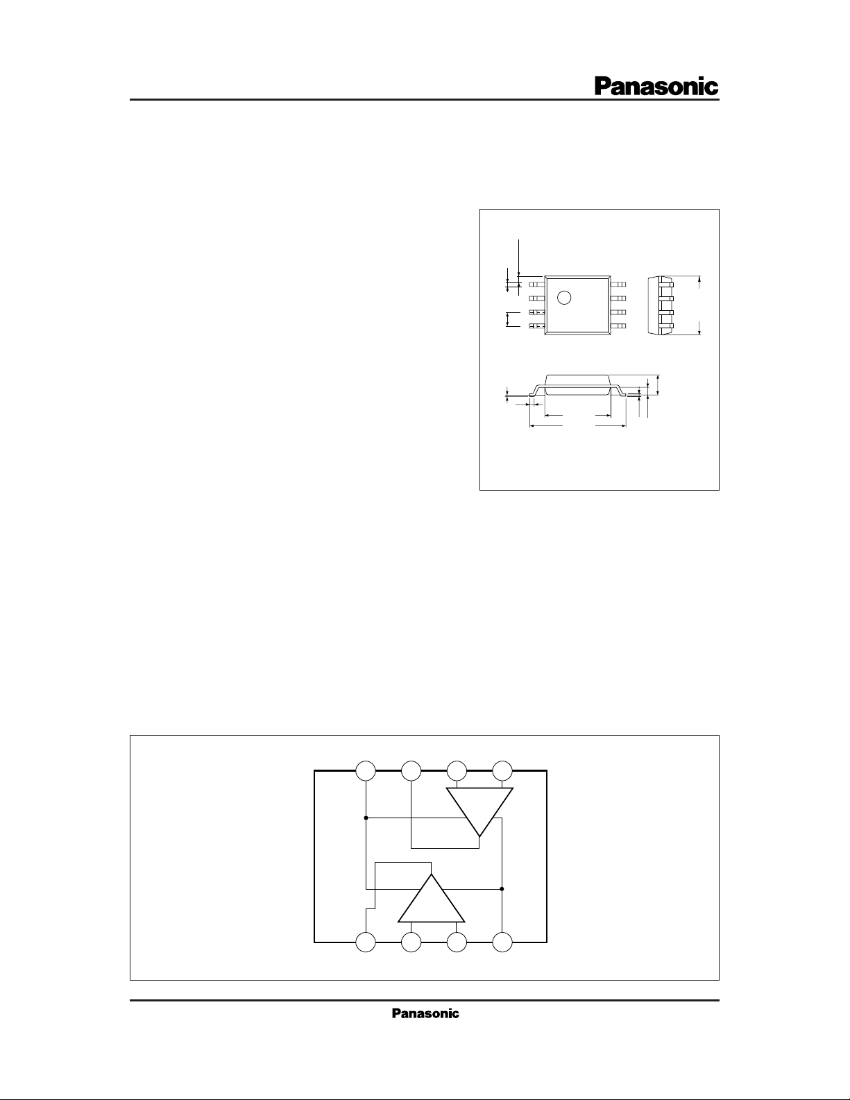
Unit:mm
0.4±0.25
1
0.6±0.31.27
2
3
4
0.1±0.1
0.3
8-pin PANAFLAT Plastic Package (SOP008-P-0225A)
4.2±0.3
6.5±0.3
8
7
6
5
1.5±0.2
0.15
0.65
5.0±0.3
■ Block Diagram
V
8
1234
V
V
CC
765
–
V
O
O
in
Ch.1
V
V
V
in
+
in
–
in
+
Ch.2
GND
Page 2
■ Absolute Maximum Ratings (Ta=25˚)
Parameter Symbol Rating Unit
Supply voltage
Commom-mode input voltage
Differential input voltage
Output applied voltage
Power dissipation
Operating ambient temperature
Storage temperature
*
1 The common-mode input voltage is applied to the non-inverting input pin and inverting input pin simultaneously.
*
2 Differential input corresponds to the potential difference between the non-inverting input pin and inverting input pin.
V
CC
V
ICM
V
V1, V
P
T
opr
T
stg
36
1
36
360
*
2
*
24
– 0.3 to +36
ID
7
D
–40 to +100
–55 to +125
■ Electical Characteristics (VCC=5V)
4
Parameter Symbol Condition min
Input offset voltage
Input offset current
Input bias current
Voltage gain
Common-mode input voltage width
Supply current
Response time
Output sink current
Output voltage low level
Output pin leak current
*
3 Typical value:Ta=25˚C
*
4 Maximum and minimum values:All the ICs are inspected at two conditional temperatures of Ta=25˚C and Ta=100˚C to
V
I
O (Leak)
I (offset)
I
IO
I
Bias
G
V
CM
I
CC
t
r
SINK
V
OL
=15kΩ
R
L
R
=∞
L
RL=5.1kΩ
=0V, VIN=1V, V
V
REF
=0V, VIN=1V, I
V
REF
=1V, VIN=0V, VO=5V
V
REF
SINK
O
<
1.5V
=
=3mA
*
0V
10I
assure the characteristics.
typ
200
3
*
max
250 nA
VCC–1.5
1.5 mA0.6
0.4 V0.2
V
V
V
V
mW
˚C
˚C
4
*
Unit
5mV1
50 nA
V/mV
mA
nA0.1
V
µs1.3
Page 3

■ Characteristics Curve
I
1.6
1.4
1.2
(mA)
1.0
CC
0.8
0.6
0.4
Supply Current I
0.2
0
0 10203040
CC –VCC
RL= ∞
Ta=–30˚C
Ta=25˚C
Ta=85˚C
Supply Voltage VCC (V)
VOL–Ta
0.24
0.20
(V)
0.16
OL
0.12
0.08
Output Voltage V
0.04
0
–40
–20
20
0
Ambient Temperature Ta (˚C)
40
=5V
V
CC
=3mA
I
SINK
80 120
60 100
I
–Ta
120
100
(nA)
80
Bias
60
40
Input Bias Current I
20
0
–20
–40
Bias
60 100
40
20
0
Ambient Temperature Ta (˚C)
Transfer Characteristic (1)
(V)
6
O
Overdrive
5
5mV
20mV
4
50mV
3
80mV
2
Output Voltage V
1
0
(mV)
IN
100
50
0
Input Voltage V
01234
VCC=5V
V
IN
Time t (µs)
–
+
=5V
V
CC
80 120
5.1kΩ
V
O
VOL– I
4.0
3.5
3.0
(V)
OL
2.5
2.0
1.5
1.0
Output Voltage V
0.5
0
0 5 10 15 20 25 30
SINK
Output Sink Current I
Transfer Characteristic (2)
(V)
6
O
5
4
3
2
Output Voltage V
1
0
(mV)
IN
0
–50
–100
Input Voltage V
Overdrive
5mV
20mV
50mV
80mV
01234
Time t (µs)
V
V
SINK
VCC=5V
IN
–
+
=5V
CC
Ta=25˚C
–30˚C
85˚C
(mA)
5.1kΩ
V
O
■ Characteristics Dispersion Charts
1.5
(mA)
1.0
CC
0.5
Supply Current I
0
–50 –25 0 25 50
I
–Ta
CC
75 100 125 150
Ambient Temperature Ta (˚C)
VCC=5V
Page 4

V
5
4
(mV)
3
2
I (offset)
1
0
–1
–2
–3
–4
Input Offset Voltage V
–5
–50 –25 0 25 50
I (offset)
Ambient Temperature Ta (˚C)
–Ta (CH–1)
75 100 125 150
VCC=5V
V
5
4
(mV)
3
2
I (offset)
1
0
–1
–2
–3
–4
Input Offset Voltage V
–5
–50 –25 0 25 50
I (offset)
Ambient Temperature Ta (˚C)
–Ta (CH–2)
VCC=5V
75 100 125 150
50
40
30
(nA)
1O
20
10
0
–10
–20
–30
Input Offset Voltage I
–40
–50
–50 –25 0 25 50
Ambient Temperature Ta (˚C)
0.40
0.35
0.30
(V)
OL
0.25
0.20
0.15
0.10
Output Voltage V
0.05
0
–50 –25 0 25 50
Ambient Temperature Ta (˚C)
IIO–Ta (CH–1)
75 100 125 150
VOL–Ta (CH–1)
75 100 125 150
VCC=5V
VCC=5V
=3mA
I
SINK
50
40
30
(nA)
IO
20
10
0
–10
–20
–30
Input Offset Voltage I
–40
–50
–50 –25 0 25 50
Ambient Temperature Ta (˚C)
0.40
0.35
0.30
(V)
OL
0.25
0.20
0.15
0.10
Output Voltage V
0.05
0
–50 –25 0 25 50
Ambient Temperature Ta (˚C)
IIO–Ta (CH–2)
75 100 125 150
VOL–Ta (CH–2)
75 100 125 150
VCC=5V
VCC=5V
=3mA
I
SINK
Page 5

VOL–Ta (CH–1)
1.0
0.9
0.8
(V)
0.7
OL
0.6
0.5
0.4
0.3
Output Voltage V
0.2
0.1
0
–50 –25 0 25 50
Ambient Temperature Ta (˚C)
■ Reliability of AN6914UBS
1. Results of Reliability Test
Test item
High-temperature operation
Leaving under high temperature
Thermal shock
Temperature cycle
VCC=5V
=10mA
I
SINK
75 100 125 150
Test condition
Ta=125˚C
=12V
V
CC
Ta=125˚C
+150˚C –65˚C
500 cycles
+125 –40˚C
10000 cycles
VOL–Ta (CH–2)
1.0
0.9
0.8
(V)
0.7
OL
0.6
0.5
0.4
0.3
Output Voltage V
0.2
0.1
0
–50 –25 0 25 50
Ambient Temperature Ta (˚C)
No.of tested pieces Total test time No. of failures
150
16000 0
120 3600
160
50
VCC=5V
=10mA
I
SINK
75 100 125 150
0
0
0
2. Failure Rate (Refer to JIS-C-5003)
Assuming that the total test time = T (No. of test pieces ×
test time) and the No. of failures = r, the failure rate can
be calculated by obtaining r/T and multiplying it by the
numerical values commensurate with the reliability level
and the number of defective ICs.
If the failure rate (FR) is calculated from the results of
the above high temperature test of the AN6914UBS,
assuming that the reliability level is 60%;
T=150 × 16000=2.4 × 10⁶ (hours)
r=0 comes to 0.92 at the level of 60%.
FR=0.92/2.4 × 106=3.8 × 10–7=380Fit
Assuming that activation energy is 1.0 eV, FR will be
38 Fit at worst (Ta=100˚C) because an acceleration
factor differs by about 1 digit between at 125˚C and
100˚C.
Assembly
Screening
Shipping
Inspection
Screening Regulations
Flow Chart
Assembly Finish
Temperature Cycle Test
High Temperature
Characteristics Inspection
Normal Temperature
Characteristics Inspection
Shipping Inspection
Condition
150˚C=30min.,
–50˚C=30min.,
Move=5min.,
Frequency=5times
Ta=100˚C
Ta=25˚C
 Loading...