

Page 1
AN6913, AN6913L
Dual Comparators
■ Overview
The AN6913 and AN6913L are dual (2-channel) comparators with a wide range of operating supply voltage.
■ Features
• Wide range of operating supply voltage
Single power supply:2 to 36V
Dual power supply:±1 to±18V
• Low circuit current:0.6mA typ.
• Wide range of common-mode input voltage
:0V to VCC–1.5V (single power supply)
• Open collector output
2.4±0.25
9
8
7
6
5
4
3
2
1
4.3±0.3
3.3±0.25
+0.1
0.3
– 0.05
+0.1
0.3
– 0.05
0.5±0.1
9
8
7
6
0.5±0.1
5
4
3
2
1
2.7±0.25
2.54
1.5±0.25
1.5±0.25
3.0±0.3
0.4±0.25
1.2±0.25
2.54
1.4±0.25
6.0±0.3
23.3±0.3
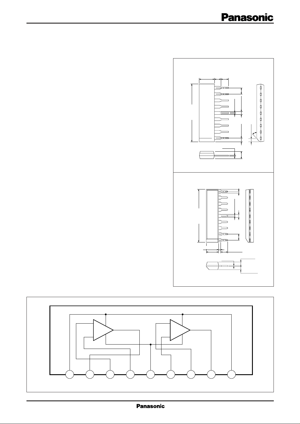
9-pin SIL Plastic Package (SIP009-P-0000C)
21.7±0.3
1.0±0.25
Unit:mmAN6913
30˚
1.4±0.3
Unit:mmAN6913L
■ Block Diagram
V
1.35±0.25
9-pin SIL Plastic Package (SIP009-P-0000A)
–
Ch.1
+
–
Ch.2
+
234567891
O1
V
in1
V
CC
–
+
V
GND
in1
+
V
in2
–
V
in2
V
O2
V
CC
Page 2
■ Pin Descriptions
Pin No.
1
Supply voltage
2
Ch.1 output
3
Ch.1 inverting input
4
Ch.1 non-inverting input
5
GND
6
Ch.2 non-inverting input
7
Ch.2 inverting input
8
Ch.2 output
9
Supply voltage
Pin name
■ Absolute Maximum Rating (Ta=25˚C)
Parameter Symbol Rating Unit
Supply voltage
Voltage
Common-mode input voltage
Differential input voltage
Output applied voltage
Power dissipation
Operating ambient temperature
Storage temperature
*
1 The common-mode input voltage is applied to the non-inverting input pin and inverting input pin simultaneously.
*
2 Differential input corresponds to the potential difference between the non-inverting input pin and inverting input pin.
V
V
ICM
VID
V1, V
T
T
CC
1
*
2
*
7
P
D
opr
stg
36
– 0.3 to +36
36
24
500
–30 to +85
–55 to +150
V
V
V
V
mW
˚C
˚C
■ Recommended Operating (Ta=25˚C)
Parameter Symbol Range
Operating supply voltage range
V
CC
■ Electrical Characteristics (VCC=5V, Ta=25˚C)
Parameter Symbol Condition min typ max Unit
Input offset voltage
Input offset current
Input bias current
Voltage gain
Common-mode input voltage width
Supply current
Response time
Output sink current
Output voltage low level
Output pin leak current
V
I
I (offset)
I
IO
I
Bias
G
V
CM
I
CC
t
r
SINK
V
OL
O (Leak)
=15kΩ
R
L
R
= ∞
L
RL=5.1kΩ, VRL=5V
V
REF
V
REF
= 0V, V
V
IN
= 0V, VIN=1V, V
= 0V, VIN=1V, I
=1V, VO=5V
REF
Single power supply 2V to 36V
Dual power supply ±1V to ±18V
200
0V
<
SINK
O
=
1.5V
=3mA
10I
5mV1
50 nA
250 nA
V
–1.5
CC
1.5 mA0.6
0.4 V0.2
V/mV
V
µs1.3
mA
nA0.1
Page 3

■ Characteristics Curve
I
Ta=–30˚C
Ta=25˚C
Ta=85˚C
CC –VCC
RL=∞
120
100
(nA)
80
Bias
60
40
Input Bias Current I
20
0
–40
1.6
1.4
1.2
(mA)
1.0
CC
0.8
0.6
0.4
Supply Current I
0.2
0
0 10203040
Supply Voltage VCC (V)
VOL– I
4.0
3.5
3.0
(V)
OL
2.5
2.0
1.5
1.0
Output Voltage V
0.5
0
051015202530 01234
Output Sink Current I
SINK
V
Ta=25˚C
–30˚C
85˚C
SINK
=5V
CC
(mA)
Transfer Characteristic (1)
6
(V)
Overdrive
O
5
20mV
4
50mV
3
80mV
2
Output Voltage V
1
0
(mV)
IN
100
50
0
Input Voltage V
I
–Ta
Bias
60 100
40
20
0
–20
Ambient Temperature Ta (˚C)
5mV
VCC=5V
V
IN
–
+
Time t (µs)
=5V
V
CC
80 120
5.1kΩ
V
O
VOL–Ta
0.24
0.20
(V)
0.16
OL
0.12
0.08
Output Voltage V
0.04
0
–20
–40
40
20
0
Ambient Temperature Ta (˚C)
Transfer Characteristic (2)
6
(V)
O
5
4
3
2
Output Voltage V
1
0
(mV)
IN
0
–50
–100
Input Voltage V
Overdrive
5mV
20mV
50mV
80mV
01234
Time t (µs)
=5V
V
CC
=3mA
I
SINK
80 120
60 100
VCC=5V
V
IN
–
+
5.1kΩ
V
O
 Loading...