

Page 1
AN-663
FOR UNIPOLAR RANGES:
DATA = ((ADC RESULT – R ADC ZS CAL. REG.) XADC FS REG./
200000h – R CH. ZS CAL. REG.) XCH. FS CAL. REG./200000h
FOR BIPOLAR RANGES:
DATA = ((ADC RESULT – R ADC ZS CAL. REG.) XADC FS REG./
400000h + 800000h – R CH. ZS CAL. REG.) XCH. FS CAL. REG./200000h
WHERE THE ADC RESULT IS IN THE RANGE OF 0 TO FFFFFh.
AND R = 1 ON 2.5 V AND 1.25 V RANGES AND R = 2 ON THE 0.625 V.
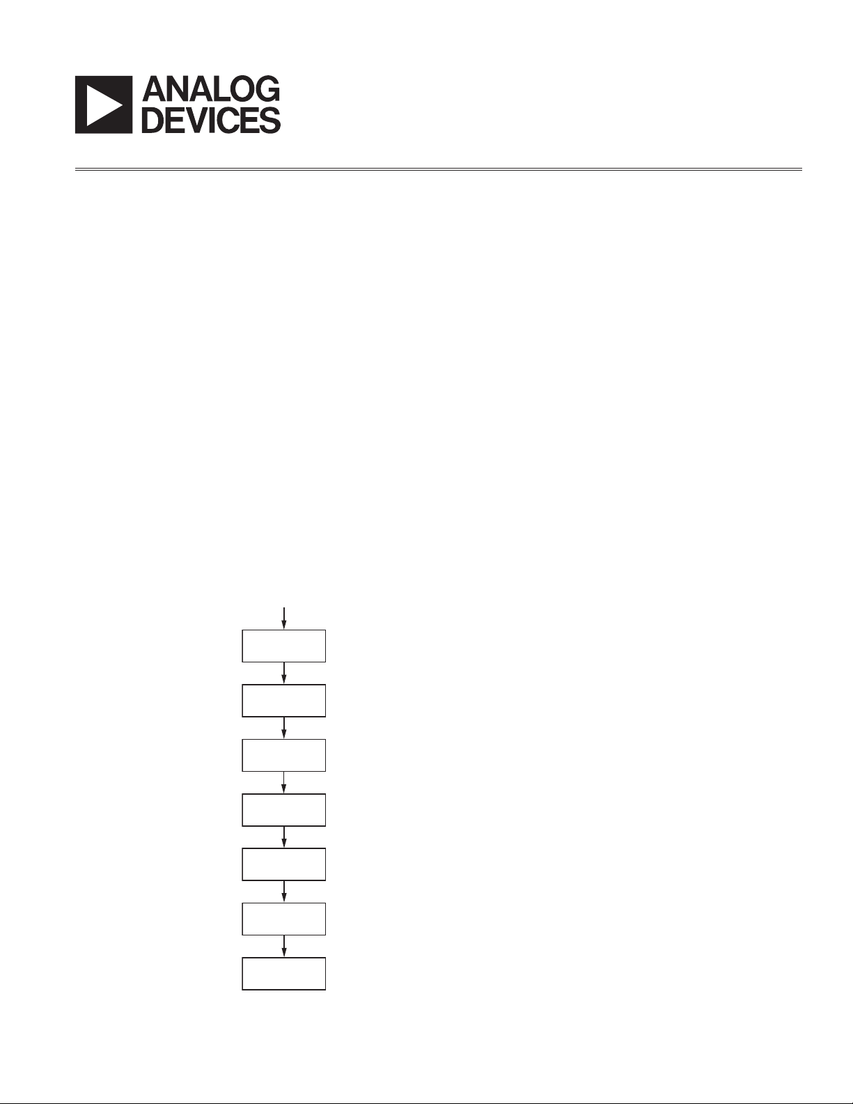
CONVERSION
DATA
AVAILABLE
SUBTRACT
ADC OFFSET
REGISTER
MULTIPLY BY
ADC GAIN
REGISTER
SUBTRACT
PER CHANNEL
OFFSET REGISTER
MULTIPLY BY
PER CHANNEL
GAIN REGISTER
APPLY CLAMP
IF SELECTED
WRITE TO
DATA REGISTER
FROM FILTER
APPLICATION NOTE
One Technology Way • P.O. Box 9106 • Norwood, MA 02062-9106 • Tel: 781/329-4700 • Fax: 781/326-8703 • www.analog.com
AD7732/AD7734/AD7738/AD7739 Calibration Registers
By Tom Meany
This application note concentrates on the AD7739 but is
also applicable to the AD7732, AD7734, and AD7738.The
purpose of this application note is to explore the calibration
registers in more detail than is found on the data sheets.
INTRODUCTION
The AD7739 features two sets of calibration registers. The
main function of these registers is to store the offset and gain
coefcients for the various calibration modes. However,
since all nine sets of registers can be read to and written
from over the serial interface, these registers are available
to manipulate raw ADC conversion results.
The rst set of registers is a 24-bit offset (ADC offset)
register and 24-bit gain (ADC gain) register, which affect
all channels. The second set includes a per channel 24-bit
offset register and a 24-bit per channel gain register, which
affect a specic channel only.
The effect of the calibration registers is independent of
conversion time, but does depend on the range. All calibration registers on the AD7732, AD7734, AD7738, and AD7739
can be read to or written from over the serial interface.
However, a write to the registers will be ignored if the ADC
is converting or calibrating when the write takes place.
This avoids corrupting the conversion result. Therefore,
you must set the ADC into its sync mode by writing 000
to the mode bits before writing to any of the calibration
registers.
Figure 1. Flow Chart for Calibration Register Contents
REV. 0
Page 2
AN-663
–3–
AN-663
REV. 0
ADC OFFSET COEFFICIENT
The shared ADC offset register is a 24-bit register used in
the calculation of all ADC results on any channel. Although
this register may be read from and written to, this register
should be modied only by self-ZS calibrations. The per
channel offset registers were provided to allow users to
manipulate the output code.
The format of the register is offset binary so that 0x000,000
is negative full-scale, 0xFFF,FFF is positive full-scale, and
0x800000 is 0. The default value of the register is 0x800000,
which results in an adjustment of zero in the output code.
The maximum absolute change is ±224.
If the mode is set to 000 and then 0x70BDC0 (minus one
million in decimal) is written to the ADC ZS register, the
effect on the output code for a 0 V input is as follows:
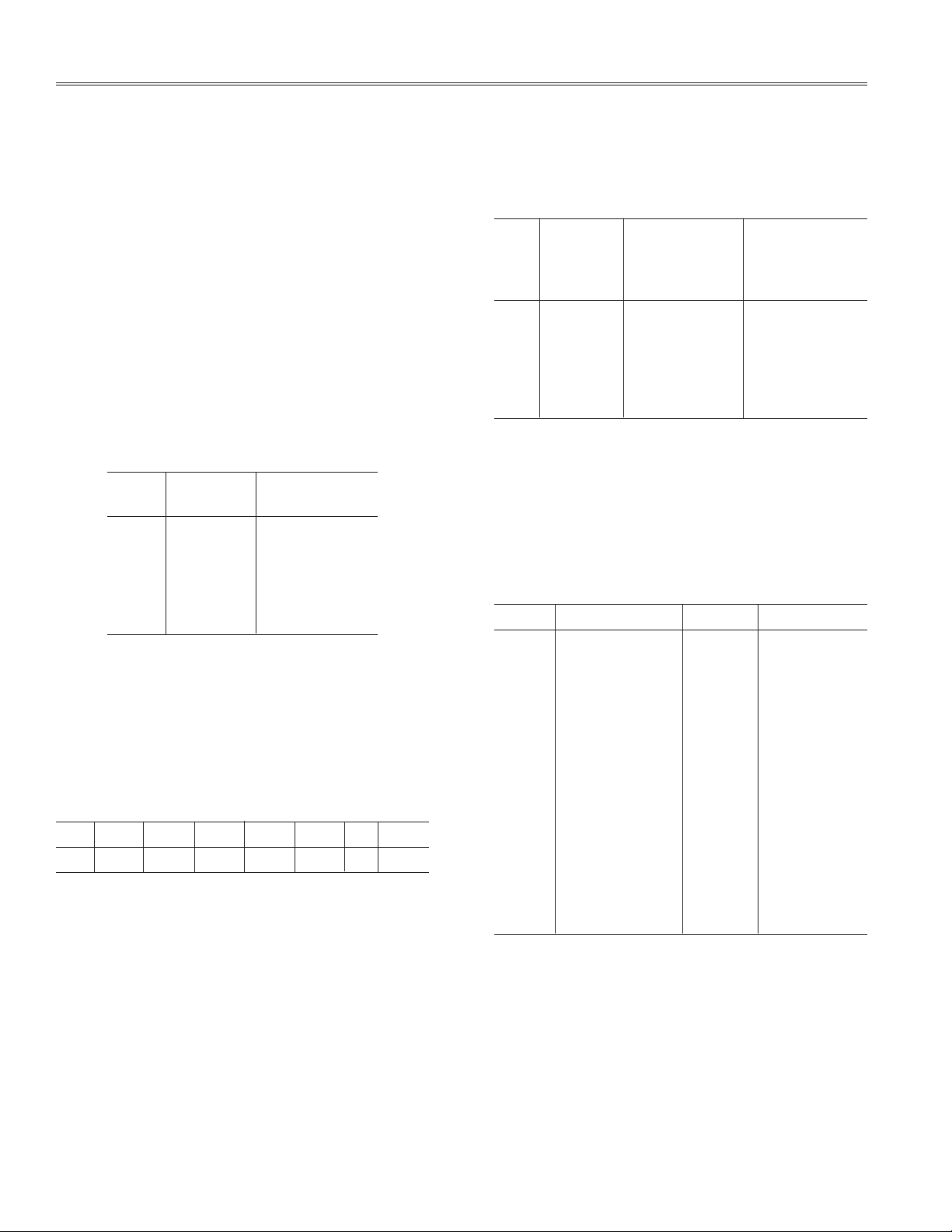
Table I. 24-Bit Output Codes for VIN = 0,
ADC Coefcient = 0x70BDC0
as Measured on Applications Board
Output Code
VIN Range Increase
0.0 ±2.5 2,000,000
0.0 ±1.25 2,000,000
0.0 ±0.625 4,000,000
0.0 0/2.5 4,000,000
0.0 0/1.25 4,000,000
0.0 0/0.625 8,000,000
ADC GAIN COEFFICIENT
The shared ADC gain register is a 24-bit register and is
used in calculating all ADC results on any channel. Although
this register may be read from and written to, this register
should be modied by only self-FS calibrations. The per
channel gain registers were provided to allow users to
manipulate the output code.
Table II. Bit Map of the ADC Gain Register
MSB MSB-1 MSB-2 MSB-3 MSB-4 MSB-5 ....... LSB
1 1/2 1/4 1/8 1/16 1/32 1/2
The range of the adjustment in gain is therefore from 0 to 2.
The default value of the register is 0x800000, which corresponds to a gain of 1.
23
If the mode is set to 000 and then 0x900,000 is written to
the ADC FS register, the effect on the output code for a
0.5 V input is as follows:
Table III. Change in Output Code Due to
Change in ADC Gain Coefcient
Output with Output with
ADC Gain ADC Gain
Coefcient Coefcient
VIN Range = 0x800000 = 0x900000
0.5 ±2.5 1,695,000 1,906,794
0.5 ±1.25 3,386,431 3,808,826
0.5 ±0.625 6,772,522 7,617,452
0.5 0/2.5 3,389,465 3,812,643
0.5 0/1.25 6,771,653 7,617,749
0.5 0/0.625 13,544,211 15,233,216
INTRODUCTION TO THE PER CHANNEL OFFSET AND GAIN COEFFICIENTS
On each of the generics there are eight sets of per channel
calibration registers, each comprised of a 24-bit offset and
a 24-bit gain register. These registers are assigned to the
physical input channels as shown in Table IV.
Table IV. Assignment of Physical Pins to
Per Channel Calibration Registers
Channel AD7738/AD7739 AD7734 AD7732
000 [AIN0, AIN1],
[AIN0, Common] AIN0 [AIN0+, AIN0–]
001 [AIN2, AIN3],
[AIN1, Common] AIN1
010 [AIN4, AIN5],
[AIN2, Common] AIN2 [AIN1+, AIN1–]
011 [AIN6, AIN7],
[AIN3, Common] AIN3
100 [AIN0, AIN1],
[AIN4, Common] AIN0 [AIN0+, AIN0–]
101 [AIN2, AIN3],
[AIN5, Common] AIN1
110 [AIN4, AIN5],
[AIN6, Common] AIN2 [AIN0+, AIN0–]
111 [AIN6, AIN7],
[AIN7, Common] AIN3
–2–
REV. 0
Page 3

AN-663
It can be seen from this table that most channel combinations have two available register sets. For example, AIN0
on the AD7738 uses channel register set 0 when converting
on channel 000, but if the conversion is done on channel
100, then it uses register set 100.
On all four generics including the AD7732, AD7734, system
zero-scale and system full-scale calibrations can be used to
remove all offset and gain errors in the signal chain including offset and gain due to the on-chip resistor matching
on the AD7732/AD7734. A system ZS calibration changes
the per channel offset coefcient for a specic channel,
and a system FS calibration changes the gain coefcient
for the selected channel. If the system ZS and the system
FS calibrations are performed in the factory and stored
in external memory, they can be downloaded to the ADC
after power-up.
PER CHANNEL OFFSET COEFFICIENT
With the per channel gain register at its default value,
increasing the offset register contents by 1 increases or
decreases the output of all future conversions on that
channel, depending on the sign bit.
Table V. Bit Map of Per Channel Offset Register
MSB MSB-1 Bits MSB-2 to LSB
Sign 0 Magnitude 0 to 2,097,151
The MSB of the per channel offset coefcient is the sign
bit. If the sign bit is 1, the offset coefcient is negative and
it causes the ADC output code to increase. If the MSB is 0,
then the offset coefcient is positive and the output code
decreases. Bit 23 of the per channel offset register must
be 0 and the remaining 22 bits are magnitude bits.
As an illustration, if 0x8F4240, sign = 1, magnitude =
1 million decimal is written to the channel 0 ZS calibration
register, the resulting change in all Channel 0 conversions
will be as shown in Table VI.
Table VI. 24-Bit Output Codes Change
Per Channel Offset Register = 0x8F4240
Output Code
VIN Range Increase
0.0 ±2.5 1,000,000
0.0 ±1.25 1,000,000
0.0 ±0.625 2,000,000
0.0 0/2.5 2,000,000
0.0 0/1.25 2,000,000
0.0 0/0.625 4,000,000
Therefore for the ±2.5 V and ±1.25 V ranges, an LSB
change in the per channel offset register corresponds to
an LSB change in the ADC output code. For the ±0.625 V,
0/2.5 V, and 0/1.25 V ranges, a 1 LSB change in the calibration register gives a 2 LSB change in the output code;
nally for the 0/0.625 V range, the change is 4 LSB.
PER CHANNEL GAIN COEFFICIENT
The default gain coefcient is 0x200000. This corresponds
to multiplying all outputs by 1. The MSB bit corresponds
to multiply by 4 and each successive bit multiplies by 2,
1, 0.5, and so on.
Table VII. Bit Map of the Per Channel Gain Register
MSB MSB-1 MSB-2 MSB-3 MSB-4 MSB-5 ---- LSB
4 2 1 1/2 1/4 1/8 1/2, 097, 152
The range of the adjustment is therefore from 0 to 8. This
allows a digital PGA to be implemented to give input ranges
smaller than ±0.625 V.
The per channel gain register is also used for system fullscale calibrations.
USE OF THE PER CHANNEL GAIN COEFFICIENT TO IMPLEMENT A PGA
The lowest available input range of the AD7739 is
±0.625 V. Suppose your signal range is only ±0.078 mV.
The default per channel gain coefcient results in the outputs shown in column 2 for the input shown in column 1. A
per channel gain coefcient of all ones results in a digital
gain of 8, and –78.125 mV corresponds to an output of all
zeros and +78.125 mV to all ones.
Table VIII. Effect of Digital PGA with Gain = 8
Output Code with Output Code with
Coefcient Coefcient
VIN = 0x800000 = 0xFFFFFF
–78 mV 0x8FF972 0xFFCB92
0 0x800000 0x800000
+78 mV 0x7FFBE9 0x00346E
The digital PGA is possible because the internal resolution
of the AD7739 is more than 24 bits and because using the
per channel gain coefcient gives access to these bits.
With a conversion time of 2.7 ms, the AD7739's output noise
on the ±0.625 V range is only 1.2 V rms or19.9 bits rms.
With a digital gain of 8, the user still has 16.9 bits of rms
resolution on the ±0.078 mV range. Another important factor for implementing a digital PGA is the 24-bit no missing
codes performance of these parts at high output rates.
REV. 0
–3–
Page 4

AN-663
PICKING COEFFICIENTS TO GIVE A SPECIFIC GAIN
If a user wants the input range to correspond to ±1.0 V, it
is necessary to pick the per channel gain coefcient. The
easiest way is to select the ±1.25 V range, put 1.0 V on the
analog input, perform a system full-scale calibration, and
record the contents of the per channel gain coefcient.
An alternative mathematical method is as follows: divide
the actual input range by the desired input range and multiple by 221, i.e., multiply 1.25 by 221 = 2621440d, which is
280000h. For this case, 1.25/1.0 is 1.25.
REMEMBER
You must set the mode bits in the mode register to 000
before writing to any of the calibration registers. Otherwise, if a calibration or conversion is in progress, the
write will be ignored.
E03816–0–7/03(0)
© 2003 Analog Devices, Inc. All rights reserved. Trademarks and registered trademarks are the property of their respective companies.
–4–
REV. 0
 Loading...