

Page 1
ICs for Motor
■ Overview
The AN6608, the AN6609N and the AN6609NS are the
electronic governors which incorporate the forward
/reverse rotation and double speed controls of the DC
motors used for radio/cassette tape recorder, and the
functions such as fast forward, rewind, brake, and pause.
They are also available for controlling the video tape deck
mechanisms such as the VCRs and DATs. The AN6608,
the AN6609N and the AN6609NS are identical with each
other except the operating logic by 3-bit input.
■ Features
•
Operating supply voltage range ; Vcc = 8V to 16V
•
Stable reference voltage (1.27V) and easy speed
adjustment
•
Large starting torque and maximum control torque
•
Built-in power transistor
•
Forward/reverse constant speed and double speed
controls, and fast forward, brake, and pause functions
available by 3-bit input
■ Applications
VCRs, cassette decks, radio/cassette tape recorders,
car cassette tape players, tape loading DC motor con
trol such as DATs.
AN6608, AN6609N, AN6609NS
DC Motor Forward/Reverse Dual Speed Electronic Governors
AN6608,
AN6609N
AN6609NS
124
12 13
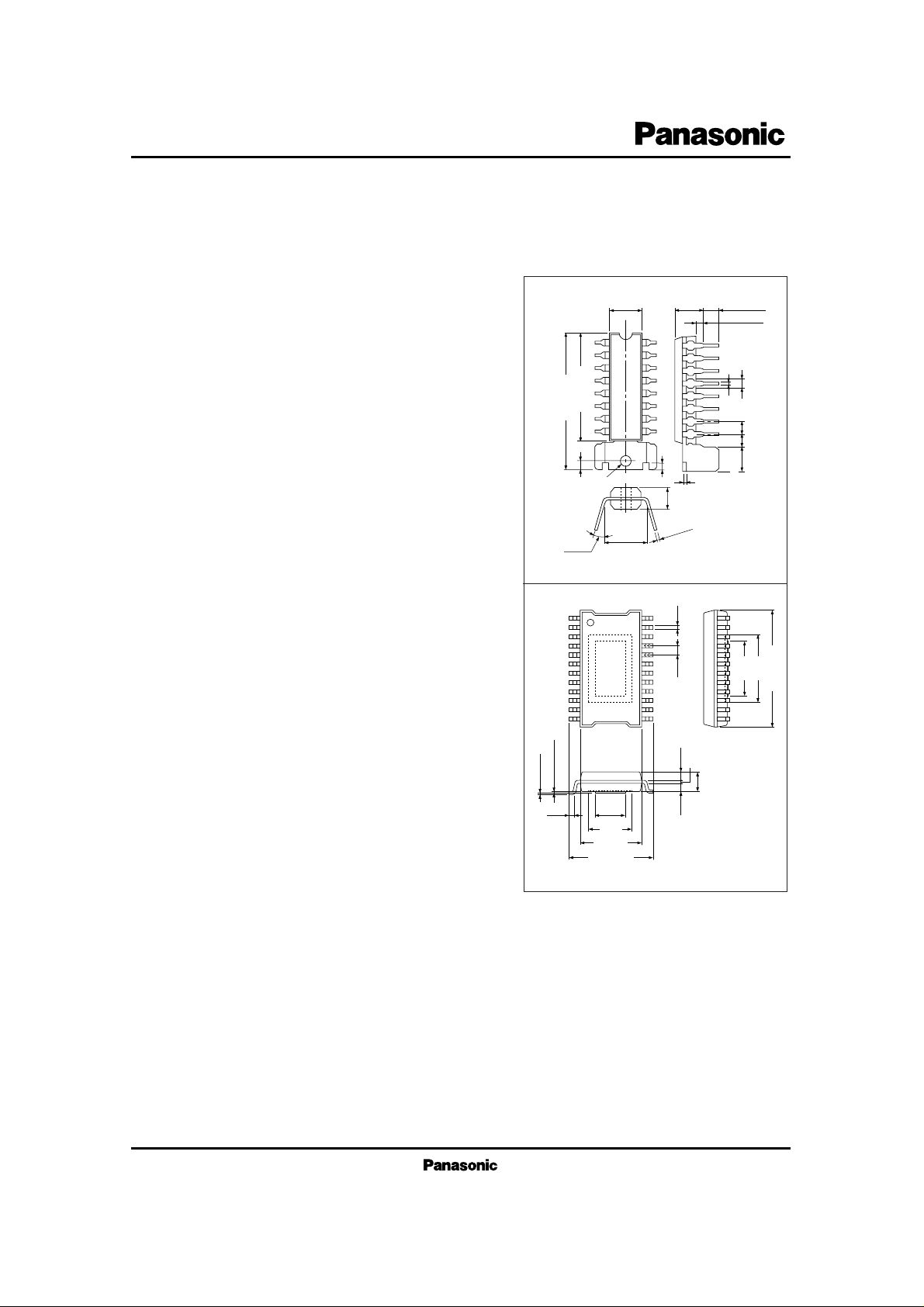
6.35±0.3 4.7±0.25
1
2
3
4
5
21.6±0.3
6
27.4±0.3
7
8
17
1.7
ø 2.1
0 ~ 6˚
7.62
16-Lead DIP Package with Fin (HDIP016-P-300)
16
15
14
13
12
11
10
9
1.5±0.1
3.80±0.3
+ 0.1
0.45
±
0.25
0.41.27
– 0.05
0.5±0.1
Unit : mm
3.05±0.25
1.06±0.25
0.1
±
0.5
0.1
±
5.08
Unit : mm
(7.8)
0.25
±
1.2
2.54
2.54
(9.2)
16.0±0.3
0.1±0.1
(0.05 ~ 0.1)
(4.6)0.5
(6.0)
8.4±0.3
11.73±0.3
24-Lead HSOP Package (HSOP024-P-0450)
(0.2)
3.15±0.2
1.45 1.45
Page 2
AN6608, AN6609N, AN6609NS
ICs for Motor
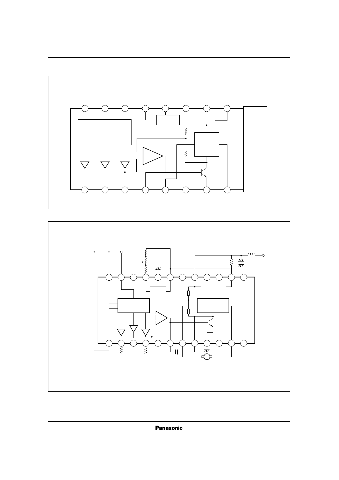
16 15 14 13 12 11 10 9
1 2 3 4 5 6 7 8
Comp.
Drive Mode
Switching Logic
V
CC
GND
V
REF
Forward/
Reverse
Drive
Circuit
1kΩ
10kΩ
GND
Fin
AN6608, AN6609N
■ Block Diagram
24 1314151617181920212223
1 12111098765432
V
REF
Comp.
M
P
1
P2P
3
V
CC
AN6609NS
P
T
Note) For motor lock, V
CC
=13V or less, Motor coil resistance = 8Ω or more,
Lock time =1s or less.
Drive Mode
Switching Logic
Forward/
Reverse
Drive Circuit
Page 3

ICs for Motor
AN6608, AN6609N, AN6609NS
■ Absolute Maximum Ratings (Ta= 25˚C)
V
CC
I
CC
T
opr
T
stg
Supply Voltage
Supply Current
Operating Ambient Temperature
Storage Temperature
V
mA
˚C
˚C
Parameter Symbol Rating Unit
18
1800
Note 1)
–20 ~ + 70
–50 ~ +150
Note 1) t ≤ 200ms
Note 2) Mounting on PCB (20mm × 20mm of copperfoil is used for heat sink)
Note 3) Glass epoxy PCB (50mm × 50mm × 1.2mm)
Power Dissipation P
D
W
2
Note 2)
2.08
Note 3)
AN6608, AN6609N
AN6609NS
Parameter Symbol Range
Operating Supply Voltage Range
V
CC
8V ~ 16V
■ Recommended Operating Range (Ta = 25˚C)
■ Electrical Characteristics (Ta = 25˚C)
VCC=12V
V
CC
=12V
Supply voltage with which a motor starts rotating
VCC=12V, N=1600rpm
V
CC
=8V, IL=55mA ~ 120mA
V
CC
=8V ~ 16V, N=1600rpm
V
CC
=12V, N=3200rpm
V
CC
=8V, IO=1A
V
CC
=8V, IO=1A
V
CC
=12V, Ta= –10˚C ~ + 60˚C
V
CC
=12V, t=15s ~ 10ms
Parameter Symbol Condition min. typ. max. Unit
7
1.27
0
0
100
0.4
Bias Current at No Load
Reference Voltage
Rated Load Start Voltage
Rated r.p.m.
r.p.m. Characteristics on Load Change
r.p.m. Characteristics on Voltage Change
Double Speed Forward/Reverse r.p.m. Difference
Output Saturation Voltage 1
Output Saturation Voltage 2
r.p.m. Characteristics on Temperature Change
r.p.m. Drift Characteristics by Time
I
bias
V
ref
V
CC (s)
N
L
DN
L
DN
V
DN
Logi
V
sat (1)
V
sat (2)
DN
A
DN
T
mA
V
V
%
rpm
rpm
%
V
V
rpm/˚C
%
1.15
6.5
–8.75
–100
–22
–3
15
1.4
8.75
100
22
3
2
1.5
■ Application Circuit
16 15 14 13 12 11 10 9
1 2 3 4 5 6 7 8
M
P
1
P2P
3
+ –
0.022µF
C
2
R
5
1.5kΩ
5kB
5.6kΩ
R
4
1kΩ
10kΩ
V
REF
Comp.
2000
ppm/˚C
R
1
11kΩ
R
2
2.7kΩ
VR
1
1kB
R
1
1.0Ω
(3900ppm/˚C)
C
1
4.7µF
–
+
L
1
47µH
V
CC
To Mechanism Control
AN6608
AN6609N
Drive Mode
Switching Logic
Forward/
Reverse
Drive
Circuit
Fin
Page 4

AN6608, AN6609N, AN6609NS
ICs for Motor
Equivalent CircuitDescription
Pin No.
1
Double Speed
Setting
Pin to set the double speed r.p.m.
Input Impedance
Pin Name
Typ. Waveform
AN6608
AN6609N
AN6609NS
2 Tr
C
2
FF, REW
Speed Setting
Pin to set the FF/REW r.p.m.
4 Tr
C
3 Speed Control
Speed control pin
A fixed resistor will do if fine
adjustment is unnecessary.
5 Tr
E
4
Phase
Adjustment
Motor
Connection
Phase adjustment pin for
oscillation prevention
6 Tr
E
5 Pin to connect the motor side7
6
Phase
Adjustment
Phase adjustment pin for
oscillation prevention
8
7 GND
Motor
Connection
GND pin for the power section
inside the IC
9
8 11
9
Load
Characteristics
Setting
Pin to set the load characteristics
(S–T curve) of the motor
14
Pin to connect the motor side
Tr
E
Tr
C
Tr
C
Tr
E
Tr
E
Tr
C
Tr
C
1
V
CC
2
V
CC
3
V
CC
4
V
CC
5
6
7
8
9
+
–
■ Pin Descriptions
+
–
Page 5

ICs for Motor
AN6608, AN6609N, AN6609NS
■ Pin Descriptions (Cont.)
Equivalent CircuitDescription
Pin No.
10
V
CC
IC power pin
Input Impedance
Pin Name Typ. waveform
AN6608
AN6609N
AN6609NS
17
11
Connect to
Pin9 .
Ref. Voltage
Output
Reference voltage output pin
when connecting to the pin9.
19 Tr
C
12
GND
GND pin for the IC bias section
20
14
Logic Input P
3
Logic input pin P
3
to set
the motor control state
23
15
Logic Input P
2
Logic input pin P2 to set
the motor control state
24
16
Logic Input P
1
Logic input pin P1 to set
the motor control state
1
60kΩ
60kΩ
60kΩ
13
Ref. Voltage
Output
Reference voltage output pin
21 Tr
C
11
12
13
V
CC
V
REF
14
60kΩ
40kΩ
15
60kΩ
40kΩ
16
60kΩ
40kΩ
+
–
–
+
Page 6

AN6608, AN6609N, AN6609NS
ICs for Motor
Input Pins
14
Output Pins (AN6608) Output Pins (AN6609N)
15 16 5 8 1 2 5 8 1 2Operating Mode Operating Mode
H H H H L OFF ON — —
OFF OFFFF Pause
L H H L H OFF ON H L ON OFFREW Double speed
H L H H L OFF OFF H L OFF OFFConstant speed Constant speed
H H L H H OFF OFF H H OFF OFFBrake Brake
L L H H L ON OFF H L OFF ONDouble speed FF
L H L L H ON OFF L H ON OFF
Reverse double speed Reverse double speed
H L L L H OFF OFF L H OFF OFF
Reverse constant speed Reverse constant speed
L L L — — OFF OFF — — OFF OFFPause Pause
* Input level H : 3V or more, Input level L : 0.7V or less
For the AN6609NS, the above pin numbers must be replaced.
PD – Ta
2.5
2.0
1.5
1.0
0.5
0
Ambient Temperature Ta (˚C)
Power Dissipation P
D
(W)
400 20 60 100 140–20 80 120 160
(1)
(2)
(1)
10mm × 20mm, with
Solder Plated Copper Foil,
H
eat Sink
(2) Without Heat Sink
PD – Ta
2,400
2,200
2,000
1,800
1,600
1,400
1,200
1,000
800
600
400
200
0
Ambient Temperature Ta (˚C)
Power dissipation P
D
(mW)
250 75 125
Glass epoxy PCB (50
× 50 ×
1.2mm)
R
thj – a
= 60˚C/W
P
D
= 2083mW (25˚C)
15010050
2,083
1,420
Without PCB
R
thj – a
= 88˚C/W
P
D
= 1420mW (25˚C)
AN6608, AN6609N AN6609NS
■ Supplementary Explanation
• Operating Logic
• Characteristics Curve
 Loading...