

Page 1
AN6567, AN6568, AN6568S
Dual High Output Current Operational Amplifiers
■ Overview
The AN6567, the AN6568, and the AN6568S are high
output current dual operational amplifiers which allows
single power supply operation, realizing lo w current consumption, high slew rate and high output current.
■ Features
• Single supply operating
• High output current:IO=70mA min.
• Low supply current:ICC=5mA typ.
• High slew rate:SR=1.0V/µs typ.
• Built-in input circuit protection
• Built-in phase compensation circuit
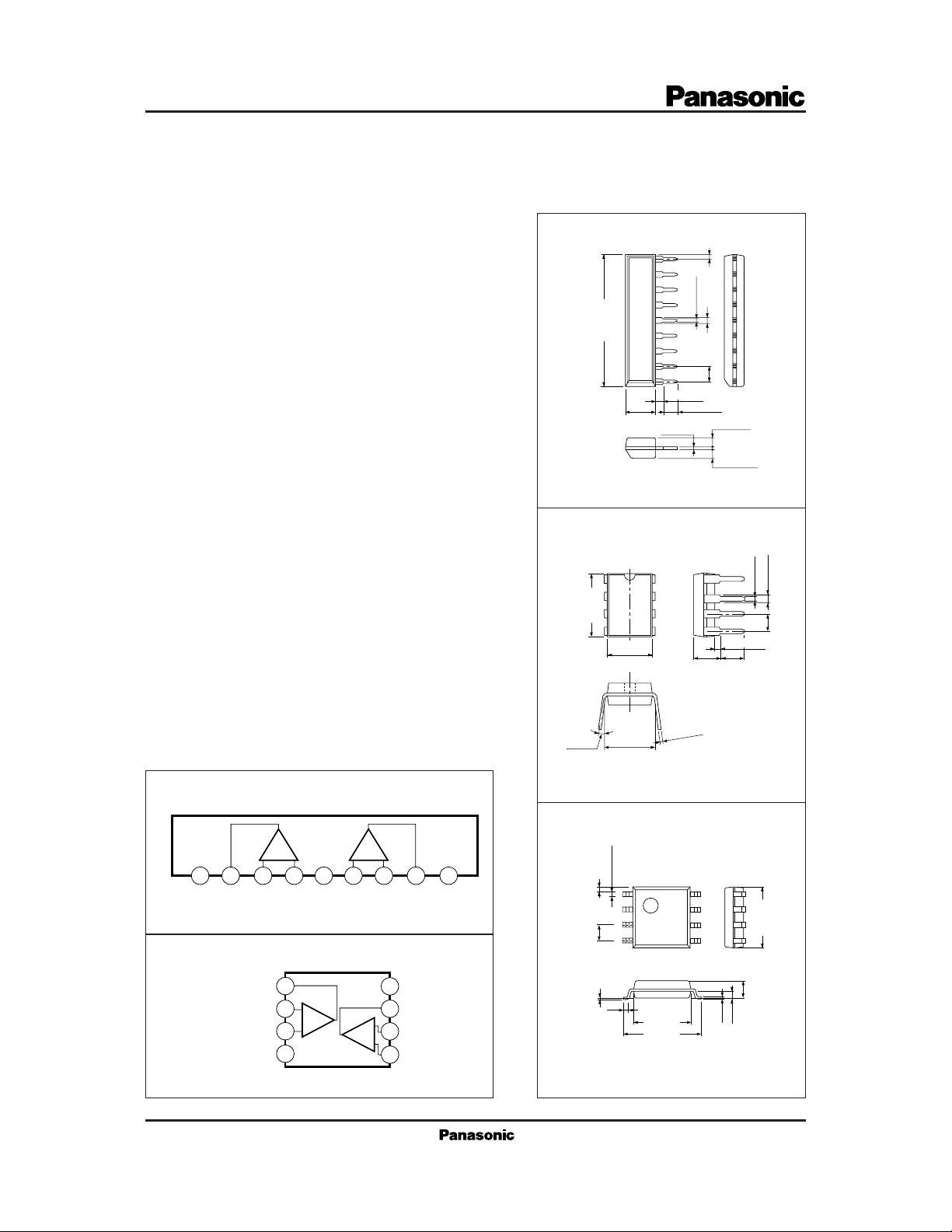
21.7±0.3
1.0±0.25
4.3±0.3
0.3
9-pin SIL Plastic Package (SIP009-P-0000A)
AN6568
1
2
3
9.4±0.3
4
8
7
6
5
6.3±0.3
9
8
7
6
0.5±0.1
5
4
3
2
1
2.7±0.25
+0.1
– 0.05
3.8±0.25 (3.45)
0.4±0.25
1.2±0.25
2.54
1.4±0.25
1.35±0.25
0.51min.
Unit:mmAN6567
Unit:mm
0.5±0.1
1.2±0.25
2.54
■ Block Diagram
AN6567
+
–
1 23456 879
V
V
CC
Note) Pin1 and Pin9 are in common.
AN6568
AN6568S
–
V
O1
in1
V
O1
–
V
in1
+
V
in1
V
EE
(GND)
V
1
2
3
4
+
in1
(GND)
–
+
+0.1
– 0.05
4.2±0.3
6.5±0.3
0.15
Unit:mmAN6568S
8
7
6
5
0.15
5.0±0.3
1.5±0.2
0.65
7.62±0.25
3
—
15˚
8-pin DIL Plastic Package (DIP008-P-0300B)
+
–
–
V
+
V
V
EE
in2
in2
8
7
–
6
+
5
V
V
CC
O2
V
CC
V
O2
–
V
in2
+
V
in2
0.4±0.25
1
0.6±0.31.27
2
3
4
0.1±0.1
0.3
8-pin PANAFLAT Plastic Package (SOP008-P-0225A)
Page 2
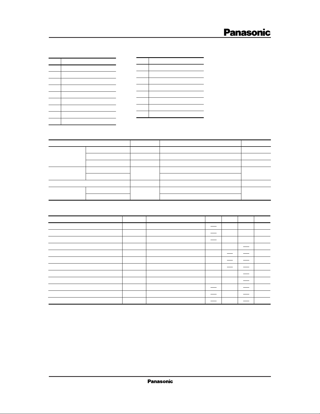
■ Pin Descriptions
〈AN6567〉
Pin No.
1
2
3
4
5
6
7
8
9
Pin name
V
CC
Ch.1 output
Ch.1 inverting input
Ch.1 non inverting input
(GND)
V
EE
Ch.2 non inverting input
Ch.2 inverting input
Ch.2 output
V
CC
〈AN6568, AN6568S〉
Pin No.
■ Absolute Maximum Ratings (Ta=25˚C)
Parameter Symbol Rating Unit
Supply voltage
Voltage
Power dissipation
Operating ambient temperature
Storage temperature
Differential input voltage
Common-mode input voltage
AN6567, AN6568
AN6568S
AN6567, AN6568
AN6568S
Pin name
1
Ch.1 output
2
Ch.1 inverting input
3
Ch.1 non inverting input
(GND)
4
V
EE
Ch.2 non inverting input
5
Ch.2 inverting input
6
Ch.2 output
7
V
8
CC
V
CC
V
ID
V
ICM
P
D
T
opr
T
stg
18 (±9)
18
– 0.3 to +18
500
360
–20 to +75
–55 to +150
–55 to +125
V
V
V
mW
˚C
˚C
■ Electrical Characteristics (VCC=15V, Ta=25˚C)
Parameter Symbol Condition min typ max
Input offset voltage
Input offset current
Input bias current
Voltage gain
Maximum output voltage I
Maximum output voltage II
Common-mode input voltage width
Common-mode rejection ratio
Supply voltage rejection ratio
Supply current
Slew rate
Zero-cross frequency
V
I (offset)
I
V
O (max.)
V
O (max.)
V
CMR
SVR
SR
f
I
IO
Bias
G
V
CM
I
CC
(T)
<
50Ω
R
S
=
<
50Ω
R
S
=
<
50Ω
R
S
=
=2kΩ
R
L
>
2kΩ, VCC=5V
R
L
=
=70mA, VCC=5V
I
O
=∞, VCC=8.3V
R
L
>
R
2kΩ, AV=1
L
=
Unit
5mV2
100
nA30
500 nA100
100
88
3.3
3.0
V
–2
CC
80
80
90
dB
V
V
V
dB90
dB
mA5
V/µs1.0
MHz1.3
Page 3

■ Characteristics Curve
120
100
80
(dB)
V
60
40
Voltage Gain G
20
0
1 10 100 1k
100
80
(nA)
IO
60
40
GV– f
10k 100k 1M 10M
Frequency f (Hz)
I
–Ta
IO
VCC=7.5V
=–7.5V
V
EE
=2kΩ
R
L
VCC=7.5V
=–7.5V
V
EE
5
4
(mV)
I (offset)
3
2
1
Input Offset Voltage V
0
–20 0 20
Ambient Temperature Ta (˚C)
500
400
(nA)
Bias
300
200
V
I (offset)
I
Bias
–Ta
–Ta
VCC=7.5V
=–7.5V
V
EE
40 60 80
=7.5V
V
CC
=–7.5V
V
EE
20
Input Offset Current I
0
–20 0 20
Ambient Temperature Ta (˚C)
15.0
12.5
10.0
(mA)
CC
7.5
5.0
Supply Current I
2.5
0
0 ±2 ±4
Supply Voltage VCC, VEE (V)
I
CC –VCC
100
Input Bias Current I
40 60 80 –20 0 20 40 60 80
0
Ambient Temperature Ta (˚C)
, V
EE
15.0
12.5
10.0
(mA)
CC
7.5
5.0
V
V
=4.3V
CC
=–4.3V
EE
I
–Ta
CC
Supply Current I
2.5
0
±6 ±8 ±10
–200 20406080
Ambient Temperature Ta (˚C)
Page 4

V
5
O (max.)
– I
O
5
V
O (max.)
–Ta
(V)
4
O (max.)
3
2
1
Maximum Output Voltage V
0
–20 0 20 40 60 80 0 20 40 60 80 100
VCC=5V
=0V
V
EE
Output Current IO (mA)
(V)
4
O (max.)
3
2
1
Maximum Output Voltage V
0
Ambient Temperature Ta (˚C)
V
CC
V
EE
=70mA
I
O
=5V
=0V
 Loading...