

Page 1
AN1358 (AN6562),
AN1358S (AN6562S)
Dual Operational Amplifiers
■ Overview
The AN1358 (AN6562)and AN1358S (AN6562S) are
dual operational amplifiers with two phase compensation circuits built-in, have a wide range of operaing supply voltage, and can operate on a single power supply.
They ha ve electrical characteristics equivalent to those
of the conventional operational amplifiers, and are lowpowered and suitable for application to various circuits.
Note) The type numbers in ( ) are old ones.
■ Features
• Built-in phase compensation circuits
• Wide range of input voltage:0V to VCC–1.5V
• Wide range of operating supply voltage:
Single power supply:3 to 30V
Dual power supply:±1.5 to ±15V
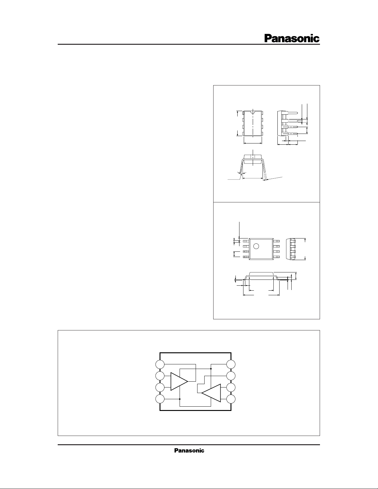
AN1358 (AN6562)
1
2
3
9.4±0.3
4
3—15˚
8-pin DIL Plastic Package (DIP008-P-0300B)
0.4±0.25
1
0.6±0.31.27
2
3
4
±0.3
6.3
7.62±0.25
8
7
6
5
0.15
3.8±0.25
+0.1
– 0.05
8
7
6
5
0.51min.
(3.45)
Unit:mm
0.5±0.1
1.2±0.25
Unit:mmAN1358S (AN6562S)
5.0±0.3
2.54
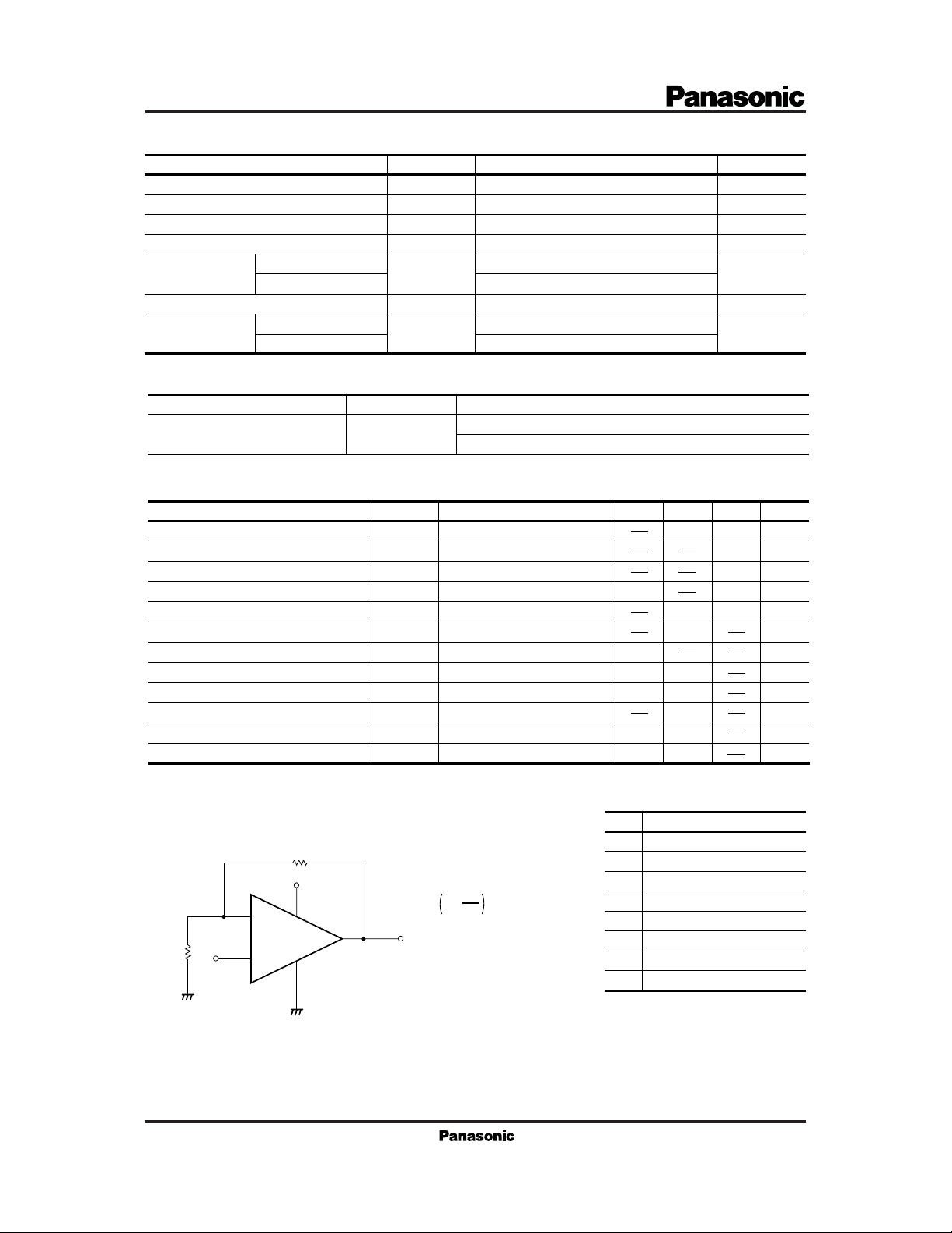
■ Block Diagram
V
O1
–
V
in1
+
V
in1
V
EE
(GND)
0.1±0.1
0.3
8-pin PANAFLAT Plastic Package (SOP008-P-0225A)
1
2
–
1
+
3
2
4
V
8
7
V
6
V
–
+
5
V
4.2±0.3
6.5±0.3
CC
O2
–
in2
+
in2
0.15
1.5±0.2
0.65
Page 2
■ Absolute Maximum Ratings (Ta=25˚C)
Parameter Symbol Rating Unit
Supply voltage
Differential input voltage
Common-mode input voltage
Output voltage
Power dissipation
AN1358 (AN6562)
AN1358 (AN6562S)
Operating ambient temperature
Strage temperature
AN1358 (AN6562)
AN1358S (AN6562S)
V
CC
V
ID
V
ICM
V
O
P
D
T
opr
T
stg
■ Recommended Operating Range (Ta=25˚C)
Parameter Symbol Range
Operating supply voltage range
V
CC
■ Electrical Characteristics (VCC=5V, Ta=25˚C)
Parameter Symbol Condition min typ max
Input offset voltage
Input bias current
Input offset current
Common-mode input voltage width
Supply current
Voltage gain
Maximum output voltage
Common-mode rejection ratio
Supply voltage rejection ratio
Channel separation
Output source current
Output sink current
V
I (offset)
I
bias
I
IO
CM
I
CC
G
V
V
O (max.)
CS dB120
I
O (source)
I
SINK
=50Ω
R
S
=∞
R
L
≥2kΩ
R
L
≥2kΩ
R
L
f=1 to 20kHz
V
in
V
in
+
=1V, V
+
=0V, V
32
32
– 0.3 to +32
24
350
360
–20 to +75
–55 to +150
–55 to +125
Single power supply 3V to 30V
Dual power supply ±1.5V to ±15V
VCC–1.5
–
=0V
in
–
=1V
in
0V
65CMR dB85
65SVR dB100
20
10
mW
7mV2
250 nA
50 nA
VCC–1.5
1.20.6
V
V
V
V
˚C
˚C
Unit
V
mA
dB100
V
mA40
mA20
■ Applica tion Circuit
Non-inverting Amplifier
–
V
in
R
1
OP. Amp.
+
■ Pin Descriptions
Pin No.
1
R
2
V
CC
V
V
O
= 1 + V
O
R
2
in
R
1
Ch.1 output pin
2
Ch.1 inverting input pin
3
Ch.1 non-inverting input pin
4
Negative supply voltage (GND)
5
Ch.2 non-inverting input pin
6
Ch.2 inverting input pin
7
Ch.2 output pin
8
Positive supply voltage
Pin name
Page 3

■ Characteristics Curve
V
5
4
(mV)
3
I (offset)
2
1
0
–1
–2
–3
–4
–5
Input Offset Voltage V
0 4 8 12 16
I (offset)–VCC
20 24 28 32
Supply V oltage VCC (V)
GV–f
120
100
(dB)
V
80
60
40
20
Voltage Gain G
0
1 100 1k 10k10 100k 1M
Frequency f (Hz)
V
Ta=25˚C
CC
=15V
IIO–V
15
10
(mA)
IO
5
0
–5
–10
Input Offset Current I
–15
0 4 8 12 16
CC
20 24 28 32
Supply V oltage VCC (V)
ICC–V
1.2
1.0
(mA)
CC
0.8
0.6
0.4
(1) Ta=–20˚C
(2) Ta=25˚C
(3) Ta=75˚C
CC
Supply Current I
0.2
0 8 12 164 20242832364044
Supply V oltage V
I
80
70
(mA)
60
bias
50
40
30
20
10
Input Bias Current I
0
0 4 8 12 16
bias–VCC
Ta=25˚C
20 24 28 32
Supply V oltage VCC (V)
I
60
(1)
(2)
(3)
(V)
CC
(mA)
50
SINK
I
O (Source)
, I
40
30
O (Source)
20
10
0
–20 20 40 600 80 100
Output Current I
Ambient Teperature Ta (˚C)
O (Source)
I
SINK
, I
SINK
–
+
V
V
in
in
–Ta
I
O (source)
VO–f
16
14
(V)
12
O
10
8
6
4
Output V oltage V
2
0
100 3k 10k1k 30k300 100k 1M300k
i
1kΩ
V
in
V
CC
2
Input Frequency fi (Hz)
–
+
100kΩ
VCC=15V
Vin, VO–t
(V)
O
V
O
2kΩ
4
3
2
1
0
(V), Output Voltage V
in
3
2
1
0
Input V oltage V
0 20406080100
V
=–15V
CC
–
V
V
I
O
+
2kΩ
Time t (µs)
140
120
(dB)
V
100
80
Voltage Gain G
60
08124 1620242832
GV–V
CC
Supply V oltage V
Ta=25˚C
(V)
CC
 Loading...