

Page 1
AN6557, AN6558, AN6558S
Dual Low Noise, High Sle w Rate Operational Amplif iers
■ Overview
The AN6557, the AN6558, and the AN6558S are low
noise, high slew rate dual operational amplifiers with
phase compensation circuits built-in. They are suitable
for application to various electronic circuits such as active filters and audio preamplifiers. Moreover, they are
high output current type and can also be used as headphone amplifiers.
■ Features
• Phase compensation circuit
• High voltage gain:GV=100dB typ.
• Low noise:Vni=0.9µVrms typ.
• High slew rate:SR=6V/µs typ.
• High output current:IO=25mA typ.
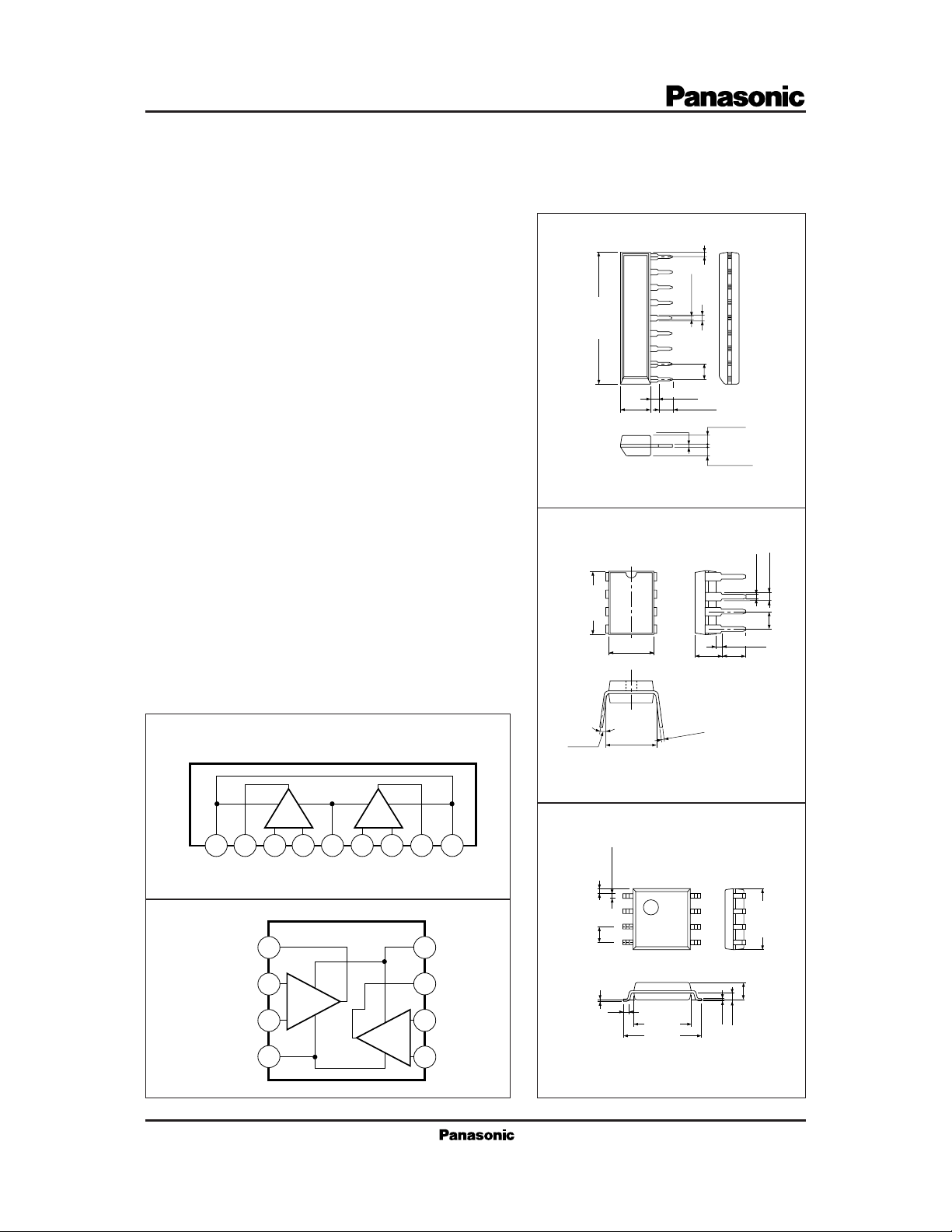
9
8
7
6
0.5±0.1
5
1.0±0.25
0.3
+0.1
– 0.05
4
3
2
1
2.7±0.25
21.7±0.3
4.3±0.3
9-pin SIL Plastic Package (Slim) (SIP009-P-0000A)
AN6558
1
2
3
9.4±0.3
4
8
7
6
5
6.3±0.3
3.8±0.25 (3.45)
0.4±0.25
1.2±0.25
2.54
1.4±0.25
1.35±0.25
0.51min.
Unit:mmAN6557
Unit:mm
0.5±0.1
1.2±0.25
2.54
■ Block Diagram
AN6557
11223456 879
V
V
O1
CC
AN6558
AN6558S
V
O1
–
V
in1
+
V
in1
V
EE
(GND)
+
–
+
–
V
V
in1
in1
1
–
2
1
+
3
4
V
EE
(GND)
+0.1
– 0.05
4.2±0.3
6.5±0.3
0.15
Unit:mmAN6558S
8
7
6
5
0.15
5.0±0.3
1.5±0.2
0.65
7.62±0.25
3
—
15˚
8-pin DIL Plastic Package (DIP008-P-0300B)
+
–
–
+
V
V
in2
in2
V
V
CC
O2
V
8
CC
V
7
O2
–
V
6
–
in2
0.6±0.31.27
0.1±0.1
0.4±0.25
1
2
3
4
0.3
2
+
+
V
in2
5
8-pin PANAFLAT Plastic Package (SO-8D) (SOP008-P-0255A)
Page 2
■ Pin Descriptions
〈AN6557〉
Pin No.
1
2
3
4
5
6
7
8
9
Pin name
V
CC
Ch. 1 output
Ch. 1 inverting input
Ch. 1 non inverting input
(GND)
V
EE
Ch. 2 non inverting input
Ch. 2 inverting input
Ch. 2 output
V
CC
〈AN6558, AN6558S〉
Pin No.
■ Absolute Maximum Ratings (Ta=25˚C)
Parameter Symbol Rating Unit
Supply voltage
Voltage
Power dissipation
Operating ambient temperature
Storage temperature
Differential input voltage
Common-mode input voltage
AN6557, AN6558
AN6558S
AN6557, AN6558
AN6558S
Pin name
1
Ch. 1 output
2
Ch. 1 inverting input
3
Ch. 1 non inverting input
(GND)
4
V
EE
Ch. 2 non inverting input
5
Ch. 2 inverting input
6
Ch. 2 output
7
V
8
CC
V
CC
V
ID
V
ICM
P
D
T
opr
T
stg
±18
±30
±15
500
360
–20 to +75
–55 to +150
–55 to +125
V
V
V
mW
˚C
˚C
■ Electrical Characteristics (VCC=15V, VEE=–15V, Ta=25˚C)
Parameter Symbol Condition min typ max
Input offset voltage
Input offset current
Input bias current
Voltage gain
Maximum output voltage
Common-mode input voltage width
Common-mode rejection ratio
Supply voltage rejection ratio
Power consumption
Slew rate
Equivalent input noise voltage
V
I (offset)
I
IO
I
Bias
V
V
O (max.)
CM
SVR µV/V10
P
C
SR V/µs
V
ni
<
10kΩ
R
S
=
>
2kΩ, VO=±10V
R
L
=
>
R
10kΩ
L
=
IO=25mA
=∞
R
L
>
R
2kΩ
L
=
=1kΩ, DIN/AUDIO
R
S
1300
86G
100
±12
±10 V±12
±12V
70CMR dB100
150
Unit
3mV0.3
200 nA10
2000 nA
dB
V±14
V±14
150
240 mW
6
µVrms0.9
Page 3

■ Characteristics Curve
GV– f
160
100k 1M 10M 100M
V
– f
ni
VCC=15V
V
Ta=25˚C
VCC=15V
V
EE
=2kΩ
R
L
=–15V
EE
140
120
(dB)
100
V
80
60
Voltage Gain G
40
20
0
0 10 100 1k 10k
Frequency f (Hz)
200
100
(nV/ Hz)
ni
50
30
20
10
5
Equivalent Input Noise Voltage V
3
0 10 100 1k 10k
Frequency f (Hz)
=–15V
V
40
35
(V)
30
O (max.)
25
20
15
10
5
Maximum Output Voltage V
0
0 10 100 1k 10k 100k 1M
O (max.)
– f
VCC=15V
=–15V
V
EE
=2kΩ
R
L
Frequency f (Hz)
I
8
7
6
(mA)
5
CC
4
3
2
Supply Current I
1
0
0246810121416
CC –VCC
VCC=–V
Supply Voltage VCC (V)
VO – I
O
=15V
V
CC
=–15V
V
EE
Ta=25˚C
(V)
O
30
25
20
15
10
Output Voltage V
5
0
0 102030405060
Load Current IO (mA)
V
Ta=25˚C
=2kΩ
R
L
O (max.) –VCC
EE
20
15
(V)
10
O (max.)
5
0
–5
–10
–15
Maximum Output Voltage V
–20
0246810121416
Supply Voltage VCC (V)
■ Applica tion Circuit
RIAA Amplifier
Input
3.3µF
15V
+
100µF
–
2.2kΩ
+–
56kΩ
47µF
+
OP. Amp.
–
–15V
30kΩ
0.0024µF 0.0082µF
+
–
610Ω
100µF
330kΩ
0.47µF
+–
2.2µF
–
+
220kΩ
 Loading...