

Page 1
AN6535
4-pin Negative Adjustable Voltage Regulator
■ Overview
The AN6535 is a monolithic 4-pin negative adjustable
voltage regulator. With an external resistor, it provides
any stabilized output v oltages between –5V and–30V , and
is optimum for the power circuits with a current capacitance of up to 0.5A. W ith various protective circuits built
in, it has high reliability and is provided in a 4-lead SIL
plastic package.
■ Features
• Wide range of output voltages:VO= –5 to –30V
• Interal thermal overload protection
• Interal short-circuit protection
• Output transistor safe area compensation
+ 0.5
9.6
– 0.1
ø 3.1
4.0
12.5max.
3–1.0
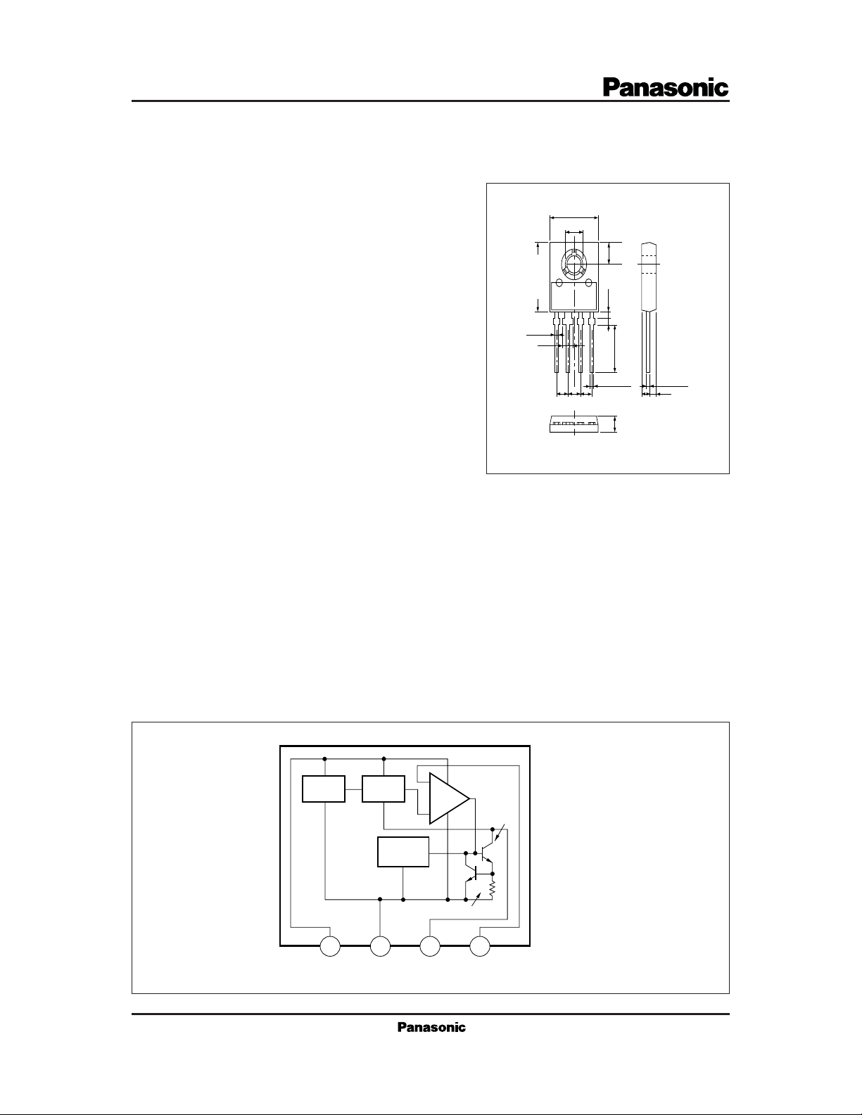
1.8
4-pin SIL Plastic Package with Fin (SSIP004-P-0000)
2.0
9.0min.
0.7±0.2 0.5±0.1
2.3 1.5 1.32.32.3
3.3max.
Unit:mm
■ Block Diagram
Start
Circuit
Common
Ref.
Voltage
Thermal
Protection
1 2 3 4
Input Output
Error
Amp.
–
Short Circuit Protection
+
Output
Pass Tr.
Rsc
Control
Page 2
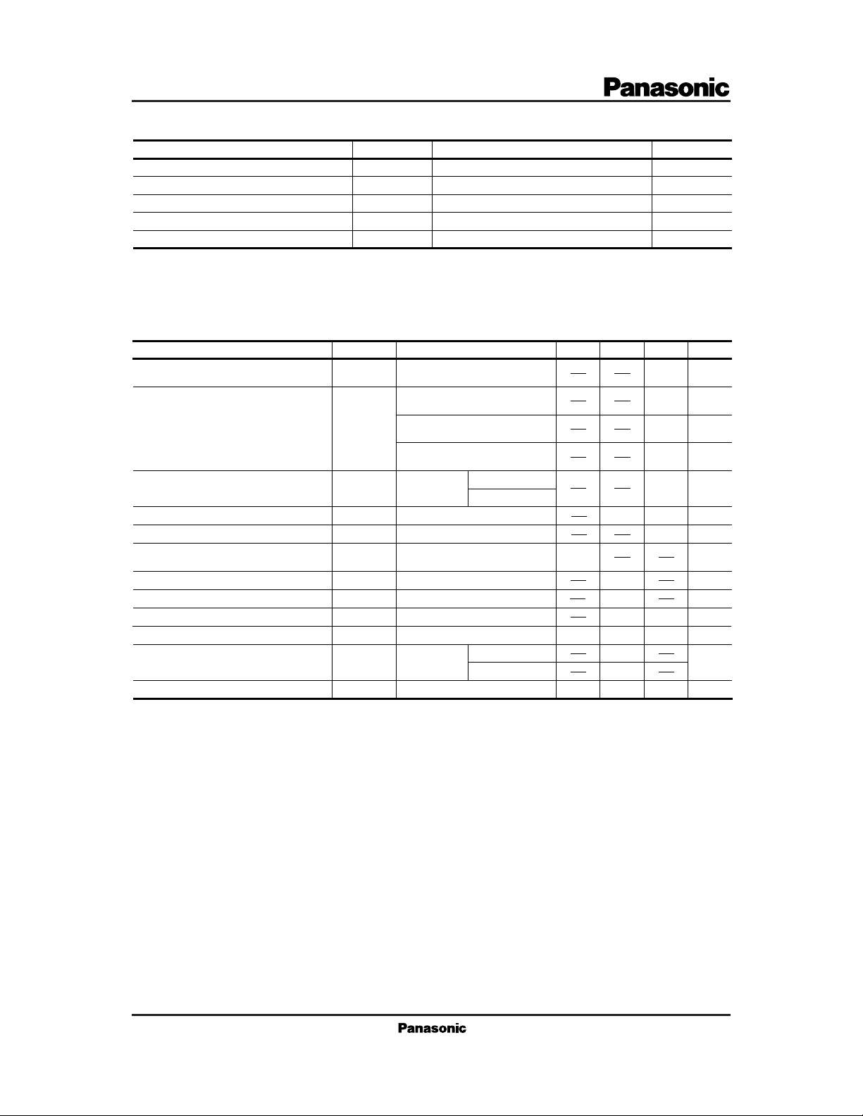
■ Absolute Maximum Ratings (Ta=25˚C)
Parameter Symbol Rating Unit
Supply voltage
Supply current
Power dissipation
Operating ambient temperature
Storage
*
1 The internal circuit is provided with a current limiting circuit.
*
2 Maximum power dissipation value when there is no heat sink (The value varies depending on the external heat dissipation state)
V
ICC
T
T
CC
1
*
P
D
opr
stg
–40
1
7.5
–20 to +80
–55 to +150
V
A
W
˚C
˚C
■ Electrical Characteristics (Ta=25˚C)
Parameter Symbol Condition min typ max
–3V to VO–15V,
V
Output voltage tolerance
Line regulation
Load regulation
Bias current
Control pin current
Ripple rejection ratio
Output noise voltage
Minimum input/output voltage difference
Short-circuit current
Peak output current
Output voltage temperatrue coefficient
Control pin voltage
V
O
REG
REG
I
Bias
I
cont
RR
V
no
V
DIF (min.)
I
OS
I
OP
∆VO/Ta
V
cont
I=VO
=5 to 350mA, Tj=25˚C
I
O
=–5V, IO=200mA,
V
O
=–7.5 to –25V, Tj=25˚C
V
I
=–18V, IO=5mA,
V
O
IN
=–21 to –33V, Tj=25˚C
V
I
=–18V, IO=200mA,
V
O
=–21 to –25V, Tj=25˚C
V
I
IO=5 to 500mA
L
Tj=25˚C
=25˚C
T
j
=25˚C
T
j
V
=–8 to –18V, VO=–5V,
I
f=120Hz
=–5V, f=10Hz to 100kHz
V
O
=500mA, Tj=25˚C
I
O
VI=–35V, VO=–5V, Tj=25
=–5V, Tj=25˚C
V
O
=–5V
V
O
=5mA Tj=25 to 150˚C
I
O
Tj=25˚C
VO=–5V, VI=–12V
VO=–18V, VI=–25V
˚C
Tj=–20 to +25
˚C
0.4
–3.12
1.5
60
40
0.2
– 0.3
–2.88
Note 1) The specified condition Tj=25˚C means that the test should be conducted with each test time reduced (within 10 ms) so that
the drift in the characteristic value due to a temperature rise at chip junction can be ignored.
Note 2) Unless otherwise specified, VI=–10V, VO=–5V, IO=350mA, CI=2µF, and CO=1µF
Unit
4%
1
%
0.75 %
0.67
%
%1
3
mA
3
µA
dB
µV
V1.1
600
1.4
mA100
A0.8
mV/˚C
V–3
Page 3

■ Characteristics Curve
PD –Ta
10
8
(W)
D
6
4
Power Dissipation P
2
0
(1) Te=Ta
(2) With a 10˚C/W heat sink
(3) With a 20˚C/W heat sink
(4) Without heat sink
(1)
(2)
(3)
(4)
0
20
40
60
80
Ambient Temperature Ta (˚C)
RR– f
120
100
80
60
100
120
140
IO=100mA
160
I
1.6
1.4
1.2
(A)
OP
1.0
0.8
0.6
0.4
Peak Output Current I
0.2
01020
OP –VDIF
I/O Voltage Difference V
Line Transient Response
V
=5V
O
10
=25˚C
T
j
30
(V)
DIF
1.4
1.2
(min.) (V)
DIF
Min. I/O Voltage Difference V
I
O
1.0
0.8
0.6
0.4
=200mA
I
O
=100mA
I
O
=10mA
–50 0 50 100 150
Juction Temperature Tj (˚C)
–20
–15
–10
Input Voltage V (V)
–5
V
DIF (min.) –Tj
I=500mA
40
20
Ripple Rejection Ratio RR (dB)
0
10 100 1k 10k 100k
Frequency f (Hz)
Load Transient Response
1
0
–1
–2
0 1020304050
Output Voltage Fluctuation (V)
Time t (µs)
0
–10
–20
0246810
Output Voltage Fluctuation (mV)
Output Current Limit
–6
(A)
O
1
–5
0.5
(V)
–4
O
VI=–10V
=–5V
V
Load Current I
0
O
=25˚C
T
j
–3
–2
Output Voltage V
–1
0
0 0.2 0.4 0.6 0.8 1.0 1.2
Output Current IO (A)
Time t (µs)
4
ZO – f
10
VI=–10V
=–5V
V
O
=20mA
I
O
=1µF
C
O
Ta=25˚C
(mΩ)
3
O
10
2
10
Output Impedance Z
10
10 100 1k 10k 100k 1M
Frequency f (Hz)
Page 4

■ Basic Regulator Circuit
+V
I
: 2µF
I
C
2
Input Output
AN6535
–
Common
+
Control
1
3
4
+V
O
VO=V
R
2
–
1µF
cont
V
O
+
C
R
1
cont
(V
≅3V, R1=3kΩ)
cont
C
: Necessary when the VI line is long.
I
CO : Improves the transient response.
■ Applica tion Circuits
(1) Current Boost Circuit (2) Current Boost Circuit
Q
6Ω
2µF
R3=
1
2
I
P
–
+
V
( β+1) I
Output
Input
AN6535
Control
Common
BE (Q1)
– I
P
· β
I
O
3
4
3kΩ
1
O
V
O
R
2
–
1µF
+
R
1
V
I
R
3
I
R
(With Current Limiting Circuit)
R
V
R
SC
I
Q
2
6Ω
3
I
R
RSC=
R3=
I
e1 (max.)=IP (max.)
R1+R
I
e1
I
e2
2µF
V
BE (Q1)
I
e1 (max.)
V
BE (Q1)+Ie1RSC
R
Q
–
+
IO – I
2
1
1
2
I
P
Output
Input
AN6535
Control
Common
e1
V
–
3
4
3kΩ
1
BE (Q1)+BE (Q1)
R
3
I
O
V
O
R
2
–
1µF
+
R
1
 Loading...