

Page 1
1
ICs for Telephone
■ Overview
The AN6472NFBP is a speech network IC which
includes a receiver noise reducing function and is most
suitable for quality cordless telephones. It incorporates a
cross-point switch controlled by serial input. It allows
speech path switching and mixing, and provides for
three- or four-person communication and other sophisticated functions. It also incorporates REC/PLAY amplifiers
with VOX circuits.
■ Features
•
The speech block can operate on line voltage, with no
external power supply, and is operational even during a
commercial power failure.
•
Incorporates a receiver noise reducing function to
improve the handset's howling margin.
•
Incorporates auto. PAD, dial mute, DC voltage regulation, and other basic speech functions.
•
The cross-point switch can be operated independently.
•
Each output of the cross-point switch can correspond to
multiple inputs, allowing three- or four-person communication.
•
The REC/PLAY amplifiers incorporate ALC and VOX
circuits.
•
Receiver volume can be increased by 6 dB or 9 dB.
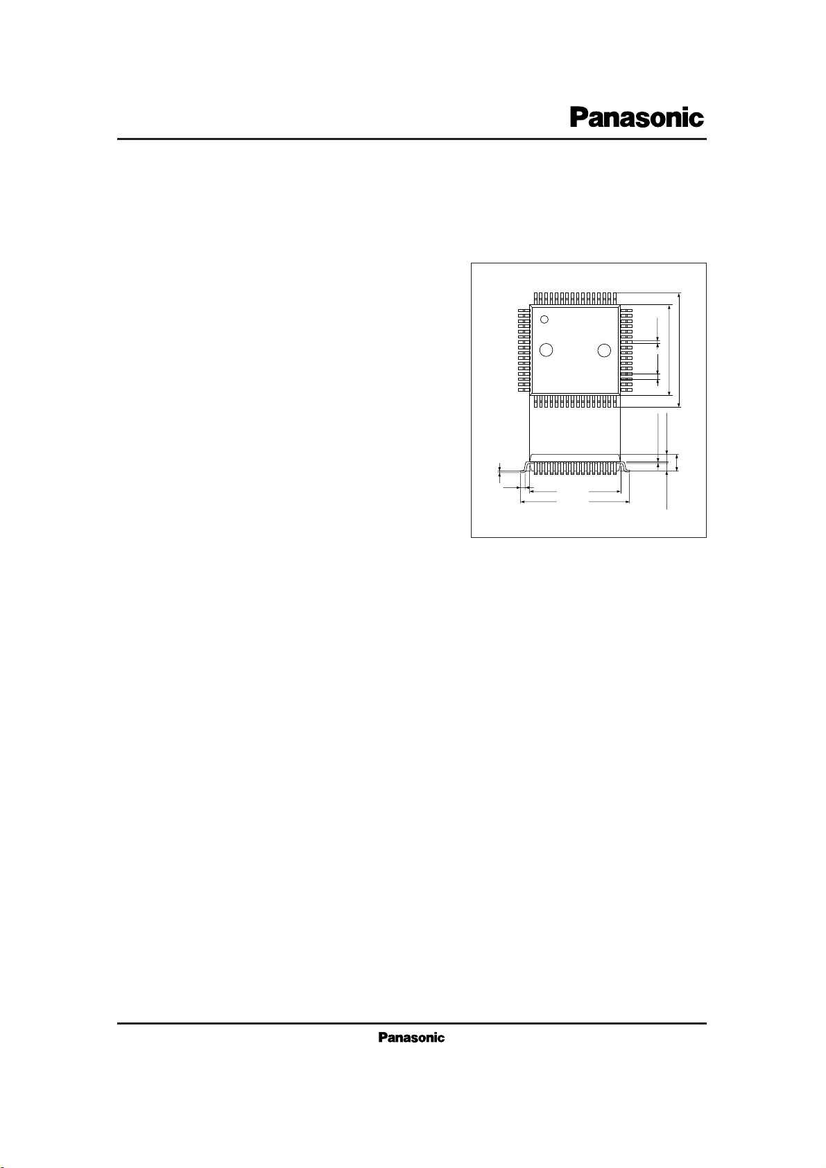
AN6472NFBP
Cordless Telephone Speech Network IC Incorporating
Cross-Point Switch
1
16
0.35±0.1
0.1±0.1
0.55
1.3±0.25
2.8±0.2
14.0±0.3
17.2±0.4
QFP package with 64 pins (QFH064-P-1414)
Unit : mm
0.15
1.3±0.25
0.8
14.0±0.3
17.2±0.4
17 32
64
48
33
49
+0.1
–0.05
Page 2
2
ICs for Telephone
AN6472NFBP
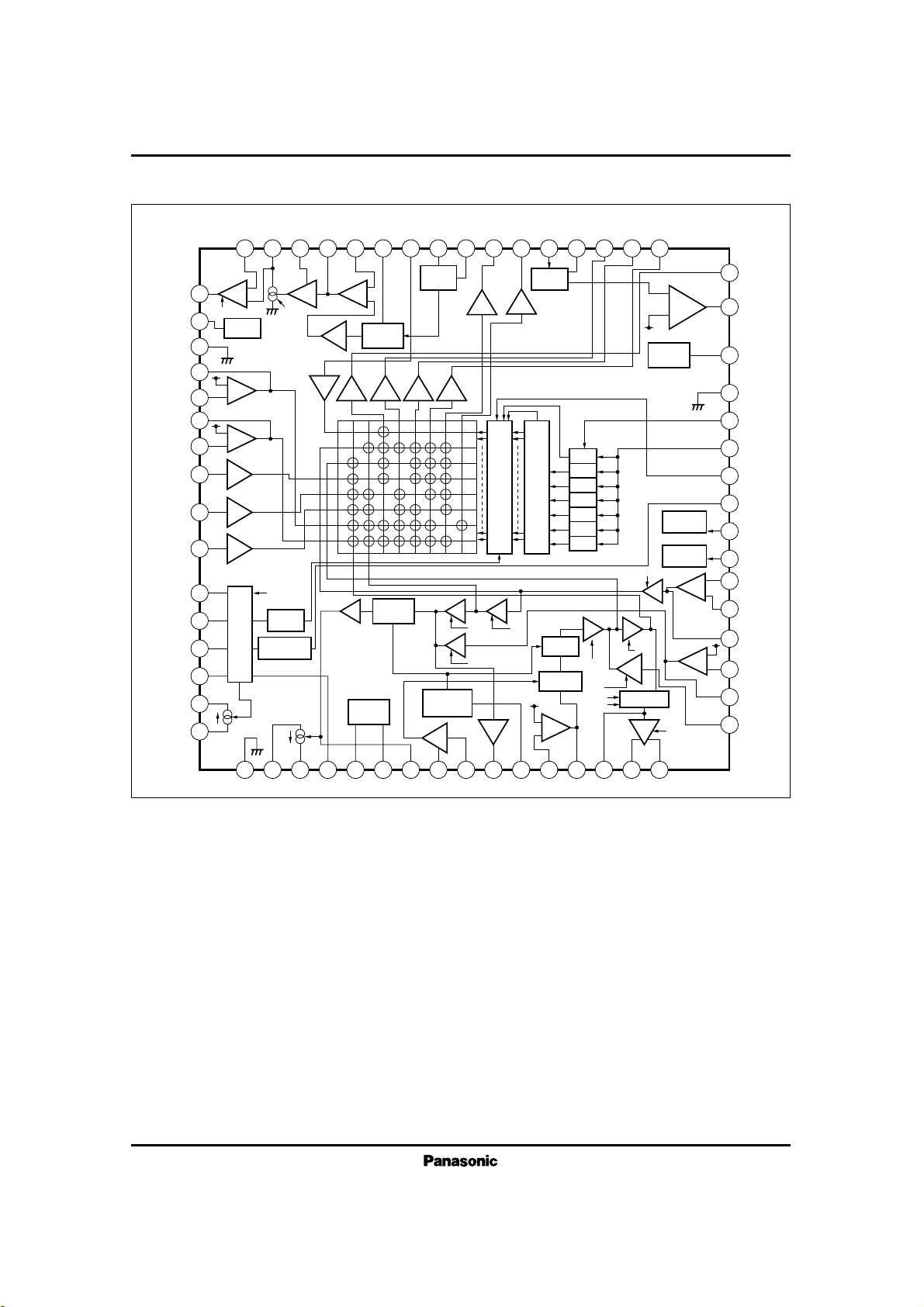
1 2 3 4 5 6 7 8 9 10 11 12 13 14 15 16
64
63
62
61
60
59
58
57
56
55
54
53
52
51
50
49
48 47 46 45 44 43 42 41 40 39 38 37 36 35 34 33
32
31
30
29
28
27
26
25
24
23
22
21
20
19
18
17
–
+
–
+
6dB
0dB
0dB
Det.
30dB
AP
Control
AP
0dB
0dB
V
REF
0dB
+–
AP
DMC
DMC VCC
0/6/9dB
L(27)
L(
17)
L(1F)
0dB
DMC
DMC
0dB
0dB
L(OF)
VCC
+–
+–
L(3F)
DC
Control
DM
Control
+
–
V
REF
+
–
L(07)
ALC
Det.
0dB
0dB
VOX
Det.
Noise
Protection
Decoder
Latch
Power Supply
Control
INJ
P.O.R
Line Supply
Monitor
D
a1
a2
a3
a4
a5
a6
COMP
ALC
10dB
0dB
0dB
0/12
dB
20
dB
18dB18
dB
DCC
GND
GND
GND
■ Block Diagram
Page 3
3
ICs for Telephone
AN6472NFBP
■ Pin Descriptions
Pin No.
Description
1
2
3
4
5
6
7
8
9
10
11
12
13
14
15
16
17
18
19
20
21
22
23
24
25
26
27
28
29
30
31
32
Ground
Line power (+) input
Side-tone adjustment
Line voltage control (1)
Int. ref. voltage output (2)
Int. ref. voltage output (1)
Trans. preamp. output
Noise reduction detection output
Noise reduction detection input
Noise reduction amp. output
Auto. PAD control
Rec. preamp. input
Rec. preamp. output
Rec. amp. input
Rec. amp. output (1)
Rec. amp. output (2)
BT signal input
DTMF preamp. output
DTMF signal input
MIC preamp. output
MIC preamp. input (1)
MIC preamp. input (2)
Dial mute control
Line voltage control
Line interruption detector output
Strobe signal input
Clock signal input
Data input
Ground
Logic power supply input
VOX detector output
SP link output
Pin No.
Description
33
34
35
36
37
38
39
40
41
42
43
44
45
46
47
48
49
50
51
52
53
54
55
56
57
58
59
60
61
62
63
64
RF2 link output
RF1 link output
Intercom link output
VOX detection control
VOX amp. input
Time stamp link output
Recording link output
ALC input
ALC detection control
Loudspeaker link input
Recording input
Recording inverse input
Recording preamp. output
Recording bias current control
To recording head
EQ amp. inverse input
EQ amp. output
REC/PLAY int. ref. voltage output
Ground
MIX preamp. output
MIX link input
AUX preamp. output
AUX link input
Intercom link input
RF1 link input
RF2 link input
Power-ON reset control
External supply voltage input
Internal supply voltage output
Circuit voltage control (2)
Line current bypass (2)
Line current bypass (1)
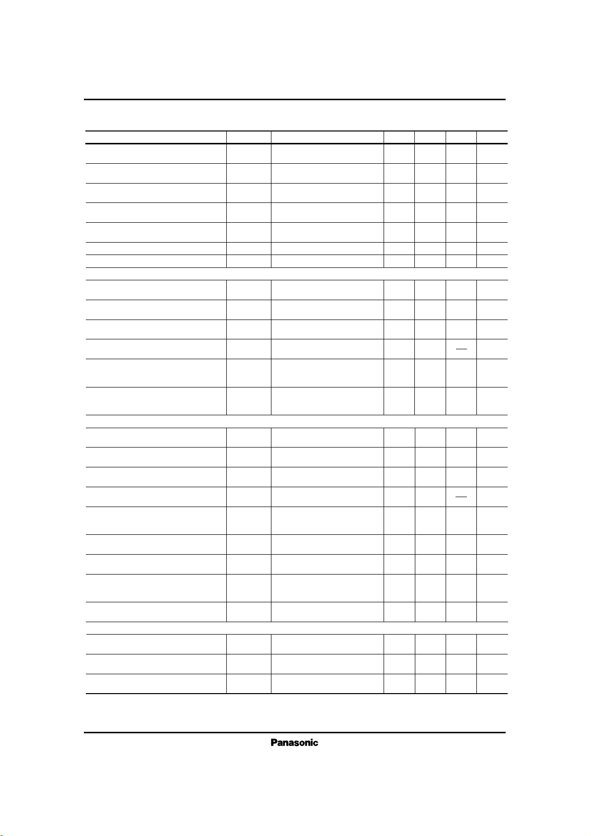
*1 In a free-air condition with Ta=75˚C
V
CC
I
CC
V
L
I
L
P
D
T
opr
T
stg
Supply voltage (1)
Supply current (1)
Supply voltage (2)
Supply current (2)
Power dissipation*1
Operating ambient temperature
Storage temperature
V
mA
V
mA
mW
˚C
˚C
Parameter Symbol Rating Unit
■ Absolute Maximum Ratings (Ta=25˚C)
7.0
50
12.0
135
640
–20 to+75
–55 to+150
Page 4
4
ICs for Telephone
AN6472NFBP
Parameter Symbol Range
■ Recommended Operating Range
Operating supply voltage range (1)
Operating supply voltage range (2)
V
CC
V
L
4.5V to 5.5V
3.0V to 11.0V
Parameter Symbol min
4.5
1.6
1.2
1.6
0.8
1.6
1.2
0.8
0.8
0
5 5.5
250
20
20
V
CC
V
kHz
µs
µs
µs
µs
µs
µs
µs
µs
µs
µs
V
typ max Unit Condition
■ Recommended Operating Conditions (Ta =20 to +75˚C)
Supply voltage
Clock frequency
Input pulse width (high)
Input pulse width (low)
Clock pulse rise time
Clock pulse fall time
Input voltage
Input pulse width
Setup time
Hold time
V
CC
f
CLK
Input Duty 40% to 50%
t
W
t
su
t
h
t
wh
t
wl
t
r
t
r
V
i
CLK
STB
DATA
STB
DATA
STB
Parameter Symbol Condition min typ max
■ Electrical Characteristics (Ta=25±2˚C)
Power Supply Characteristics During Power Failure
Normal power supply characteristics
Line DC voltage (I-1)
V
L – I1
V3.5 3.83.2
Unit
V–DCC=HIGH,
IL=20mA, VCC=0V
Line DC voltage (E-1)
V
L – E1
V3.4 3.83.1
V– DCC=HIGH,
IL=20mA, VCC=5V
Line DC voltage (E-2)
V
L – E2
V4.7 5.14.3
V–DCC=HIGH,
IL=20mA, VCC=5V
V
L – E3
V6.8 7.36.3
V–DCC=HIGH,
IL=20mA, VCC=5V
Line DC voltage H (E-1)
V
LH – E1
V4.85 5.44.3
V–DCC=HIGH,
IL=20mA, VCC=5V
Line DC voltage (I-2)
V
L – I2
V4.8 5.24.5
V–DCC=HIGH,
IL=60mA, VCC= 0V
Line DC voltage (I-3)
V
L – I3
V7.0 7.56.6
V–DCC=HIGH,
IL=120mA, VCC= 0V
Line DC voltage H (I-1)
V
LH – I1
V5.0 5.54.5
V–DCC= LOW,
IL=30mA, VCC= 0V
Line DC voltage H (I-2)
V
LH – I2
V6.2 6.75.7
V–DCC= LOW,
IL= 60mA, VCC= 0V
Line DC voltage H (I-3)
V
LH – I3
V8.5 9.27.9
V–DCC= LOW,
IL=120mA, VCC= 0V
Internal supply voltage (I)
V
reg – I
V2.0 2.21.8
V– DCC=HIGH,
IL=20mA, VCC= 0V
Internal ref. supply voltage (I)
V
ref – I
V1.0 1.10.9
V–DCC=HIGH,
IL=20mA, VCC= 0V
Line DC voltage (E-3)
Page 5
5
ICs for Telephone
AN6472NFBP
Parameter Symbol Condition min typ max
■ Electrical Characteristics (cont.) (Ta=25±2˚C)
Receiver During Power Failure
Line DC voltage H (E-2)
V
LH – E2
V5.95 6.65.3
Unit
V–DCC=LOW,
I
L
=60mA, VCC=5V
Rec. gain (I-1)
G
V – IR1
dB32.5 34.530.5
IL=30mA, VCC= 0V
Vin= – 42dBm
Rec. gain (I-2)
G
V – IR2
dB29 3127
IL= 80mA, VCC= 0V
Vin= –42dBm
Rec. auto. PAD width (I)*1
A
P – IR
dB3.5 52.5
IL=30mA– 80mA, VCC= 0V,
Vin= – 42dBm
Rec. max. output (I)
Rec. noise reduction (I)
V
O – IR
N
L – IR
dBm40
4
19
6
21
8
23
dB
dB
With IL=30mA, VCC= 0V, and
THD=5%
I
L
=30mA, VCC= 0V,
Vin= –42dBm
Vin–M= –65/–50dBm
I
L
=30mA, VCC= 0V,
V–DMC=LOW,
Vin= –30dBm
Line DC voltage H (E-3)
V
LH – E3
V8.2 8.97.55
V–DCC=LOW,
IL=120mA, VCC=5V
Internal supply voltage (E)
V
reg – E
V4.85 5.04.6
V–DCC=HIGH,
IL=20mA, VCC=5V
Internal ref. supply voltage (E)
V
ref – E
V2.5 2.72.25
V–DCC=HIGH,
IL=20mA, VCC=5V
Total circuit current
Power interruption detection (1)
Power interruption detection (2)
I
total
V
– HIT1
V
– HIT2
mA27 3517
0
4.4
0.1
4.95
0.6
5
V
V
V–DCC=HIGH,
IL=20mA, VCC=5V
VL=2.7V, VCC=5V
V
L
=1.5V, VCC=5V
G
V – IBT
Receiver On External Power Supply
Transmitter Amp. During Power Failure
Rec. gain (E-1)
G
V – ER1
dB32.5 34.530.5
IL=30mA, VCC=5V
Vin= –42dBm
Trans. gain (I-1)
G
V – IM1
dB30.2 32.228.2
R=27Ω(Pin3), IL=30mA,
VCC=0V, Vin= –38dBm
Trans. gain (I-2)
G
V – IM2
dB26.4 28.424.4
IL=80mA, VCC=0V,
Vin= –38dBm
A
P – IM
dB3.8 52.5
IL=30mA–80mA, VCC=0V,
Vin= –38dBm
Rec. gain (E-2)
G
V – ER2
dB28.8 30.826.8
IL=30mA, VCC=5V
Vin= –42dBm
Rec. auto. PAD width (E)*1
A
P – ER
dB3.7 52.5
IL=30mA–80mA, VCC=5V
Vin= –42dBm
Rec. max. output (E)
V
O – ER
dBm124
With IL=30mA, VCC=5V, and
THD=5%
Rec. noise reduction (E)
N
L – ER
dB8106
IL=30mA, VCC=5V,
Vin= –42dBm
Vin–M= –65/–65dBm
Rec. digital volume (1)*2
G
V – DV1
dB675
IL=30mA, VCC=5V,
V
in
= –42dBm, DV–1 ON
Rec. digital volume (2)*2
G
V – DV2
dB9 10.57.5
IL=30mA, VCC=5V,
Vin= –42dBm, DV–2 ON
BT amp. gain (E)
G
V – EBT
dB21.5 23.519.5
I
L
=30mA, VCC=5V,
V–DMC=LOW,
Vin= –30dBm
Rec. gain difference
DG–R dB– 0.1 1.2–1.2
For V
CC
=0V and 5V(between
Gv–IR1 and Gv–ER1)
BT amp. gain (I)
Trans. auto. PAD width (I)*1
Note) Unless otherwise specified, input signal Fin =1kHz, control voltage V-DOC = high, and control voltage V-DMC = high.
*1 Gain decrease when line current I
L
is changed from 30 to 80 mA. If pin 11 (auto. PAD control)is connected to pin 61 (int.
supply voltage output), the gain will not change.
*2 Gain increase from receiver gain (E-1).
Page 6
6
ICs for Telephone
AN6472NFBP
Parameter Symbol Condition min typ max
■ Electrical Characteristics (cont.) (Ta=25±2˚C)
Transmitter Amp. On External Power Supply
Trans. max. output (I-1)
V
O – IM1
dBm3.50
Unit
With I
L
=30mA, VCC= 0V and
HD=5%
DTMF max. output (I-1)
V
O – ID1
dBm3.80
IL=30mA, VCC=0V,
V–DMC=LOW, THD=5%
Trans. gain (E-1)
G
V – EM1
dB30.6 32.628.6
IL=30mA, VCC= 0V,
Vin= –38dBm
Trans. gain (E-2)
G
V – EM2
dB27.0 29.025.0
IL=80mA, VCC=5V,
Vin= –38dBm
Trans. auto. PAD width (E)*1
A
P – EM
dB452.5
IL=30mA–80mA, VCC=5V,
Vin= –38dBm
Trans. max. output (E-1)
V
O – EM1
dBm62
With IL=30mA, VCC=5V and
THD=5%
Trans. max. output (E-2)
V
O – EM2
dBm62
IL=30mA, VCC=5V,
THD=5%, V–DCC=LOW
Trans. max. output (I-2)
V
O – IM2
dBm3.50
With IL=30mA, VCC= 0V,
THD=5% and V–DCC=LOW
DTMF gain (I-1)
G
V – ID1
dB19.5 21.517.5
IL=30mA, VCC= 0V,
V–DMC= LOW,
Vin= –30dBm
DTMF gain (I-2)
G
V – ID2
dB15.7 17.713.7
IL=80mA, VCC= 0V,
V–DMC=LOW,
V
in
= –30dBm
DTMF max. output (I-2)
V
O – ID2
dBm3.50
IL=30mA, VCC= 0V,
THD=5%, V–DMC=LOW,
V–DCC=LOW
DTMF auto. PAD width (I)*1
A
P – IDT
dB3.8 52.5
IL=30mA–80mA, VCC= 0V,
V–DMC= LOW,
Vin= –30dBm
DTMF gain (E-1)
G
V – ED1
dB20.1 22.118.1
IL=30mA, VCC=5V,
DM=ON, Vin= –30dBm
DTMF max. output (E-1)
V
O – ED1
V
O – ED2
dBm62
IL=30mA, VCC=5V,
V–DMC=LOW, THD=5%
Trans. gain difference
DG – M dB–0.8 0.7–1.8
For V
CC
= 0V and VCC=5V
(between Gv–IM1 and Gv–EM1)
DTMF gain difference
DG – MF dB–1.3 0.2–2.3
For V
CC
= 0V and 5V
(between Gv–ID1 and Gv–ED1)
DTMF gain (E-2)
G
V – ED2
dB16.5 18.514.5
I
L
=80mA, VCC=5V,
V–DMC=LOW,
Vin= –30dBm
DTMF auto. PAD width (E)*1
A
P – EDT
dB4.1 5.52.5
IL=30mA–80mA, VCC=5V,
V–DMC=LOW,
Vin= –30dBm
DTMF max. output (E-2)
dBm62
I
L
=30mA, VCC=5V,
DM=ON, V–DMC=LOW,
THD=5%
Note) Unless otherwise specified, input signal Fin=1 kHz, control voltage V-DOC=high, and control voltage V-DMC=high.
*1 Gain decrease when line current IL is changed from 30 to 80 mA. If pin 11 (auto. PAD control) is connected to pin 61(int.
supply voltage output) , the gain will not change.
Page 7

7
ICs for Telephone
AN6472NFBP
Parameter Symbol Condition min typ max
■ Electrical Characteristics (cont.) (Ta=25±2˚C)
Recording Preamplifiers
Recording Amplifier
Playing EQ Amplifier
VOX Detector
Rec. preamp. gain
G
V – Rp
dB45 4743
Unit
V
in
= – 60dBm, Rin=0Ω
Head bias current
I
– REC
µA180 215145
L–SW (h07)= ON
VOX sensitivity (1)
VS1 V4.83.5
I–VOX=12.5µA
VOX sensitivity (2)
VS2 V0.025 0.5
I–VOX=24.5µA
Head output
G
V – REC
mVrms
50.0 63.040.0
L–SW (h07)= ON,
V
in
= –15dBm, RL=1kΩ
EQ amp. gain
G
V – EQ
dB29.8 31.827.8
L–SW (h07)= ON,
V
in
= – 40dBm
EQ amp. output noise voltage
V
no – EQ
mVrms
0.45 1.2
L–SW (h07)= ON,
DIN/AUDIO, RL=1kΩ
Rec. preamp. output
V
O – RP
dBm–11.4 –9.4–13.4
V
in
= – 45dBm, Rin=10Ω
Rec. preamp. output noise voltage*1
V
no – RP
mVrms
0.8 2.5
DIN/AUDIO, Rg=10kΩ
Link SW Input Amplifier
Link SW Output Amplifier
MIX amp. gain
G
V – MIX
dB675
Vin= – 36dBm
SP output gain (1)*1
G
V – SPO1
dB12 1311
Input AUX IN, V
in
= – 36dBm,
L–SW (h3A) = ON
SP output gain (2)*1
G
V – SPO2
dB– 0.5 0.5–1.5
Input AUX IN, V
in
= – 36dBm,
L–SW (h3A&h2F) = ON
Intercom output gain*1
G
V – DHO
dB20 21.518.5
Input AUX IN, V
in
= – 36dBm,
L–SW (h3B) = ON
RF1 output gain*1
G
V – RF10
dB18 19.516.5
Input AUX IN, V
in
= – 36dBm,
L–SW (h3C) = ON
RF2 output gain*1
G
V – RF20
dB18 19.516.5
Input AUX IN, V
in
= – 36dBm,
L–SW (h3D) = ONΩ
Recording output gain*1
G
V – RECO
dB0 1.0–1.0
Input AUX IN, V
in
= – 36dBm,
L–SW (h3E) = ON
Recording output gain*1
G
V – RO
dB21.4 22.919.9
Input AUX IN, V
in
= – 36dBm,
L–SW (h38) = ON
Line output gain*1
G
V – TO
dB19.2 20.717.7
Input AUX IN, V
in
= – 36dBm,
L–SW (h39) = ON
Rec. output gain difference*2
GD
– RO
dB0 1.0–1.0
Input AUX IN, V
in
= – 36dBm,
L–SW (h30) = ON
Time stamp output gain*1
G
V – TSO
dB0 1.0–1.0
Input AUX IN, V
in
= – 36dBm,
L–SW (h37) = ON
AUX amp. gain
G
V – AUX
dB675
V
in
= – 36dBm
Note) Unless otherwise specified, external supply voltage V
CC
=5V, line current IL= 0mA, input signal frequency=1 kHz, control
voltage V-DOC=high, and control voltage V-DMC = high.
*1 Each amp. gain is measured from AUX OUT or MIX OUT to its output (the AUX or MIX preamp. gain is not included in the
calculation).
*2 The difference from the receiver output gain (Gv-RO).
Page 8

8
ICs for Telephone
AN6472NFBP
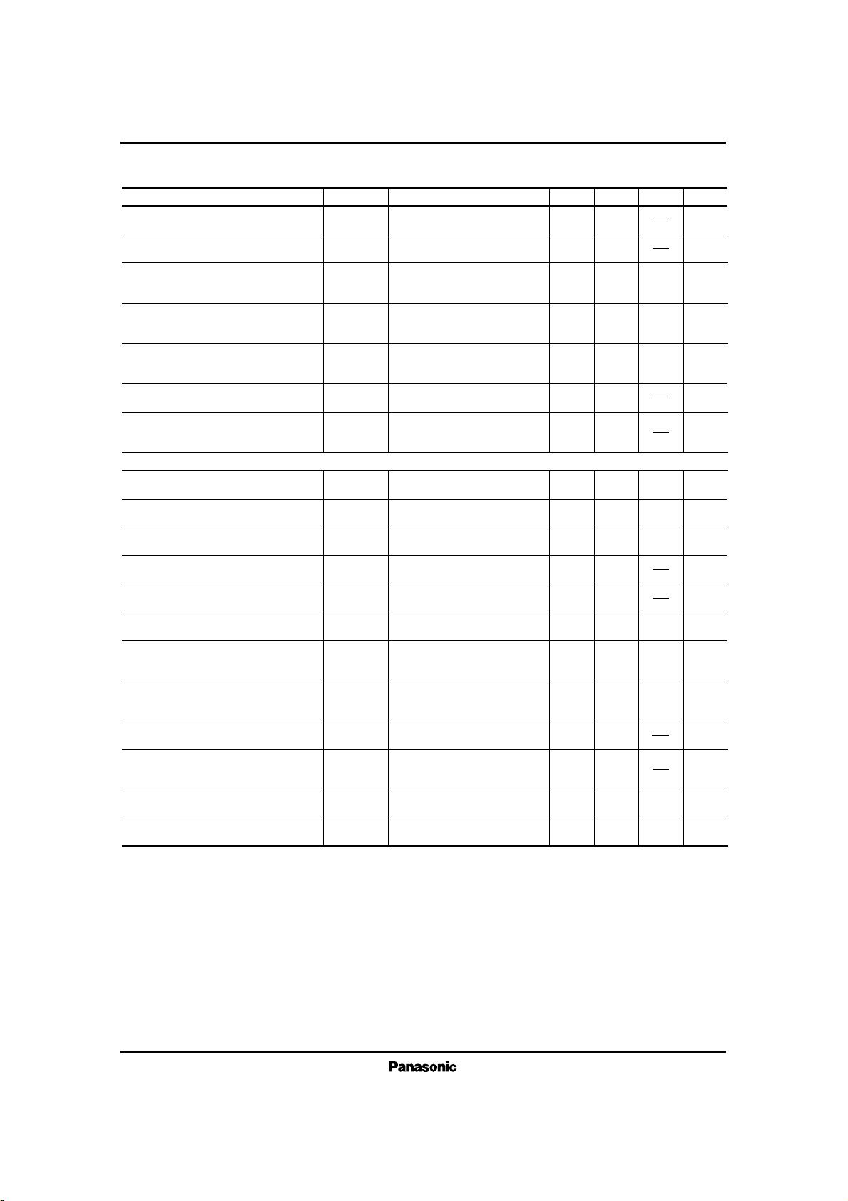
Parameter Symbol Condition min typ max
Link SW Input
MIC input gain*1
G
v – MI
dB01–1
Unit
Vin= –38dBm, rec. output
L –SW(h0E)= ON
Rec. input gain*1
G
v – RI
dB01–1
V
in
= –42dBm, rec. output
L–SW (h16)= ON
Intercom input gain
G
v – DHI
dB675
Vin= –30dBm, rec. output
L–SW (h1E)= ON
RF1 input gain
G
v – RF1I
dB01–1
01–1
V
in
= –30dBm, rec. output
L–SW (h26)= ON
RF2 input gain
G
v – RF2I
dB
Vin= –30dBm, rec. output
L–SW (h2E)= ON
SP link input gain
G
v – SPI
dB12 1311
Vin= –30dBm, SP rec. output
L–SW (h02)= ON
Link Maximum Output
SP OUT max. output
V
o – SP
dBm40
Input L–SP IN, THD=5%
L–SW (h02)= ON
DH OUT max. output
V
o – DH
dBm40
Input RF1 IN, THD=5%
L–SW (h23)= ON
RF1 OUT max. output
V
o – RF1
dBm40
Input RF2 IN, THD=5%
L–SW (h25) = ON
RF2 OUT max. output
V
o – RF2
dBm40
Input RF1 IN, THD=5%
L–SW (h2C)= ON
L-REC OUT max. output
V
o – LR
dBm40
Input AUX IN, THD=5%
L–SW (h3E)= ON
■ Electrical Characteristics (cont.) (Ta=25±2˚C)
Note) Unless otherwise specified, external supply voltage VCC=5V, line current IL= 0mA, input signal frequency=1 kHz, control
voltage V-DOC= high, and control voltage V-DMC= high.
*1 Each amp. gain is measured from MIC OUT or R PRE OUT to its output.
Parameter Symbol Condition min typ max
Controls
V
DMC – H
V2
Unit
Dial mute high level voltage
I
DMC – H
µA38 8015
Dial mute high level control current
V
DMC – L
V0.3– 0.2
Dial mute low level voltage
I
DMC – L
µA–20 –10– 40
Dial mute low level control current
V
DCC – H
V2
DC voltage control high level voltage
V
CC
+ 0.2
V
CC
+ 0.2
I
DCC – H
µA25 5010
DC voltage control high level
control current
V
DCC – L
V0.4– 0.2
DC voltage control low level voltage
V– DMC = 5V
V– DMC= 0V
V – DCC= 5V
V– DCC= 0V
I
DCC – L
µA– 0.1–2
DC voltage control low level
control current
Note) Unless otherwise specified, VCC=5V, and IL = 20 mA.
■ Electrical Characteristics (cont.) (Ta=25±2˚C)
Page 9

9
ICs for Telephone
AN6472NFBP
V
DIN – H
V2
I
DIN – H
µA160 25070
V
DIN – L
V0.3– 0.2
V– DIN=5V
V– DIN = 0V
I
DIN – L
µA– 0.1–1
Data input high level voltage
V
CC
+ 0.2
Data input high level control current
Data input low level voltage
Data input low level control current
450
Power Supply Block
AC impedance (I)
Z
AC – I
570 750
450 580 750
IL=80mA, VCC= 0V,
Vin=200mVrms, Fin=1kHz
AC impedance (E)
Z
AC – E
Ω
Ω
I
L
=80mA, VCC=5V,
Vin=200mVrms, Fin=1kHz
■ Electrical Characteristics (cont.) (Ta=25±2˚C)
Input impedance
Pin 56 Input
Z
in – DH
kΩ9.5 10.58.5
Intercom preamp. input impedance
Z
in – RF2
Pin 58 Input
RF2 preamp. input impedance
kΩ9.5 10.58.5
Z
in – RF1
Pin 57 Input
RF1 preamp. input impedance
kΩ9.5 10.58.5
Z
in – BT
Pin 17 Input
BT amp. input impedance
kΩ9.5 10.78.7
Z
in – ALC
Pin 40 Input
ALC amp. input impedance
kΩ9.5 10.58.5
Z
in – SP
Pin 42 Input
SP input impedance
kΩ50.0 62.537.5
Parameter Symbol Condition min typ max Unit
■ Electrical Characteristics (Design Values for Reference) (Ta=25±2˚C)
The following are design values for reference, not guaranteed values.
Speech Block
Rec. output noise voltage (I)
V
n – IR
mVrms0.3
IL=30mA, VCC=0V,
DIN/AUDIO
Rec. output noise voltage (E)
V
n – ER
mVrms0.3
I
L
=30mA, VCC=5V,
DIN/AUDIO
Trans. output noise voltage (I)
V
n – IT
mVrms0.3
IL=30mA, VCC=0V,
DIN/AUDIO
Trans. output noise voltage (E)
V
n – ET
mVrms0.3
I
L
=30mA, VCC=5V,
DIN/AUDIO
Dial mute trans. amp. mute attenuation
M
– TDM
dB 75
I
L
=30mA, VCC=5V,
Vin= –30dBm,
V– DBM–H/L
Rec. output mute attenuation
M
– RO
Zin
– R
dB 50
I
L
=30mA, Vin= –30dBm,
VCC=5V,
Lsw (h27)= OFF/ON
Pin 12 Input
Rec. preamp. input impedance
kΩ500
Zin
– M
Pin 21 and 22 Input
MIC preamp. input impedance
kΩ500
IL=30mA, Vin= –30dBm,
VCC=5V,
Lsw (h3F)=OFF/ON
Trans. preamp. mute attenuation
M
– TM
dB70
REC/PLAY Block
ALC amp. ALC width
W
– ALC
dB40
IL= 0mA, VCC=5V,
and ALC output distortion≤2%
ALC amp. ALC effect
DALC dB1
I
L
=0mA, VCC=5V, and
Vin= –45dBm to –20dBm
Rec. amp.
mute attenuation
M
– REC
dB 80
V
CC
=5V, Vin= –10dBm
IL= 0mA, and
LSW (h07)= ON/OFF
Parameter Symbol Condition min typ max Unit
Page 10

10
ICs for Telephone
AN6472NFBP
The following are design values for reference, not guaranteed values.
■ Electrical Characteristics (Cont.) (Design Values for Reference) (Ta=25±2˚C)
M
–EQ
VCC=5V, Vin= –30dBm
IL= 0mA,
LSW(h0F)=ON/OFF
Pin 43 input
dB80
Rec. preamp. input impedance
EQ amp. mute attenuation
Z
in–REC
kΩ10
VCC=5V, IL=30mA, AC output
measured at link ON/OFF
Link SW mute attenuation M
–LS
dB75
Pins 47 and 48 inputEQ amp. input impedance Z
in–EQ
kΩ500
VCC=5V, IL=30mA, cross talk
to line during VOX
VOX cross talk V
OX–CT
dBm–70
Pin 47 inputVOX amp. input impedance Z
in–VOX
kΩ500
Pin 53 inputMIX preamp. input impedance Z
in–MIX
kΩ500
Pin 55 inputAUX preamp. input impedance Z
in–AUX
kΩ500
Pin 25 inputCPC output impedance Z
out–CPC
kΩ100
Pin 9 inputNoise reduction amp. input impedance Z
in–NL
Ω45
Link Switch
Parameter Symbol Condition min typ max Unit
■ Pin Descriptions
Waveform Description Remarks
Pin No.
Pin name
I/O Equivalent circuit
1
2
3
4
5
6
7
I
O
I
O
O
O
GND
VL
ST
Vref
Ground :
•This is the ground pin for the
speech network.
GND for REC/PLY,
VREG, SPEECH and
LINK
Line power input:
•Connects to the positive output of the diode bridge.
Side-tone adjustment:
•
Grounded through
R1 (27Ω)
•Connects to the side-tone
adjusting circuit to adjust side
tone and receiver level.
Line voltage control (1) :
Int. ref. voltage output (2) :
•Output impedance=50Ω
Int. ref. voltage output (1) :
•Outputs half the Vreg reference
voltage.
Trans. preamp. output :
•C7 as connected between this
pin and the ground forms a
low-pass filter.
Vref–
SN
T–
FILTER
VL–
CONT
DC
3 ∼10V
DC
0.3V
DC1V
(Const)
1V
(Const)
1V
0V
DC1V
TO
2
3
–
+
5
6
61
24kΩ
24
kΩ
Vreg
6kΩ
4
7
G =
Z
Line
//Z
Tel
R
1
G= 20log
300
= 20.9db
27
The line drive gain (G) is :
Also assuming
Z
Line
≈600Ω
Z
Tel
≈600Ω
R1= 27Ω
C2 and the internal resistance
determine the f. characteristics.
Grounded through a
0.01µF capacitor.
Note) The symbols are the same as those used in the application circuit.
Page 11

11
ICs for Telephone
AN6472NFBP
■ Pin Descriptions (cont.)
Waveform Description Remarks
Pin No.
Pin name
I/O Equivalent circuit
8
9
10
11
12
13
14
15
·
16
17
18
19
I
O
I
I
O
O
O
I
O
I
APC
RV IN
•
Noise reduction detection amp. output : A smoothing capacitor C6 and
R5 connect to this pin to adjust the
attack and recovery times of noise
reduction.
•
Noise reduction detection amp. input
: Noise reduction amp. output is fed
through C7 and R6 to this pin.
•Noise reduction amp. output :
Connects to the noise reduction
detection amp. input.
Auto. PAD control :
•
Connects through a resistance to Pin
6
1(Vreg). If the resistance increases,
the PAD operates closer to the near
end. If the resistance decreases, the
PAD operates closer to the far end.
Rec. preamp. input :
•Receiver signals are input from
the side-tone circuit to this pin.
•R8 and C9 connected between
Pin 13 and this pin determine
the f. characteristics.
Rec. preamp. output :
•
R8 and C9 connected between Pin 12
and this pin determine the f. characteristics.
•
The output impedance is up to 1 kΩ.
Rec. amp. input :
Rec. amp. outputs (1 and 2) :
•A ceramic or dynamic receiver
is connected.
•The output circuit is a BTL
configuration.
•The output impedance is up to
50 Ω.
BT signal input :
•BT (beep tone) signals are input
through C15 to this pin.
•Input impedance is 10 kΩ.
DTMF preamp. output :
•A C/R combination between
Pin 19 and this pin determines
the f. characteristics of the
DTMF preamp.
DTMF signal input :
•DTMF signals are input
through a capacitor to this pin.
•DTMF signals are enabled
when DMC is low at Pin 40.
VN
DET–
IN
RV
PREOUT
BT–
IN
MF –
IN
RV
FILTER
RV
OUT
(1)
RV
OUT
(2)
MF –
OUT
VN
OUT
Vreg-R · I
IL
VN
DET
V
REF
– SN
V
REF
– SN
Signal input
V
REF
– SN
Signal input
G =
64K
R6
•
This pin must be
grounded if noise
reduction is not used.
•
The greater C7, the longer the attack time. The
smaller R6, the shorter
the recovery time.
•
Noise reduction detec-
tion amp. gain (G) is :
1
1 1
G = –
R9 + jωC9
R8 + jωC10
In the application circuit,
MIC. IN (–) is input
through a capacitor. This
capacitor and R12-R14,
and C15 and C16 determine the f. characteristics.
The 10
kΩ input impe-
dance and C12 or C13
form a HPF.
DC (with a capacitor)
Input
V
REF
V
REF
– SN
V
REF
– SN
V
REF
– SN
V
REF
– SN
–
+
8
64kΩ
Vref–SN
–
+
10
3kΩ
Vref–SN
9
0.1µF
95kΩ
I
I∝ I
L
11
–
+
13
12
–
+
10kΩ
13
–
+
30kΩ
10kΩ
15
16
13
–
+
17
10kΩ
Vref–SN
–
+
18
–
+
19
18
Vref–SN
10kΩ
V
REF
– SN
Full-wave detection
(with no capacitor)
Pin
8
output
The receiver preamplifier
gain (G) is :
Page 12

12
ICs for Telephone
AN6472NFBP
20
21
22
23
24
25
26
27
28
O
I
I
I
I
O
I
I
I
DMC
CPC
STR
CLK
DATA
MIC preamp. output :
•R12 and C14 connected
between Pin 22 and this pin
determine the f. characteristics.
•The output impedance is up to
1 kΩ.
MIC preamp. input (1) :
•A bias resistor and a microphone connect to this pin.
MIC preamp. input (2) :
•R12 and C14 connected
between Pin 20 and this pin
determine the f. characteristics.
Dial mute control :
•Normal speech mode when
Pin 23 is high or open (MIC
amp. ON and rec. amp. ON).
•DTMF mode when Pin 23 is
low (DTMF amp. ON and BT
amp. ON).
Line voltage control :
•Line voltage is normal when
the input voltage at this pin is
high. Line voltage increases
by 1-1.5 V when the input
voltage is low.
Line interruption detector output :
•
This is an open collector output to a
microprocessor, requiring a pull-up
resistor connected to the microprocessor's power supply. This pin goes
low when line voltage is 3.0 V or
more, and goes high when 1.5 V or
less.
Strobe signal input :
•The strobe signal for serial
control data is input to this
pin. The rising edge of the
strobe signal determines the
timing at which internal control address or ON/OFF status
is validated.
Clock signal input :
•
The clock signal for serial control
data is input to this pin. The rising
edge of the clock signal determines
the timing at which data is read.
Data input :
•Serial data is input to this pin.
Data is read into the internal
shift register in synchronization with clock signals.
MIC
OUT
MIC
IN
(+)
MIC
IN
(–)
DC –
CONT
V
CC
0.2V
Line DC voltage
L–V
CC
0.2V
Line interruption
0V
5V
0V
5V
0V
5V
V
REF
– SN
–
+
10kΩ
Vref
–
+
20
21
22
61
100kΩ
23
200kΩ
200kΩ
150kΩ
24
26
300kΩ
L–V
CC
10kΩ
27
300kΩ
L–V
CC
10kΩ
300kΩ
L–V
CC
10kΩ
28
2
25
56kΩ
L–V
CC
144kΩ
VL
100kΩ
V
REF
– SN
V
REF
– SN
■ Pin Descriptions (cont.)
Waveform Description Remarks
Pin No.
Pin name
I/O Equivalent circuit
Page 13

13
ICs for Telephone
AN6472NFBP
29
30
31
32
33
34
35
36
37
38
39
O
O
O
O
O
O
I
O
O
GND
Ground :
•This is the ground pin for the
logic circuits.
Logic power supply input :
V
OX detector output :
•This is an open collector out-
put.
•This pin goes high when voice
signals are input to Pin 37.
Loudspeaker link output :
•This is a link switch output to
an external loudspeaker amplifier.
•The output amplifier gain is
selectable between 12 and 0
dB.
•Output impedance is 50±
30Ω.
RF2 link output :
•This is a link switch output.
•Output impedance is 50Ω.
RF1 link output :
•This is a link switch output.
•Output impedance is 50Ω.
Intercom link output :
•This is a link switch output to
an intercom.
•Output impedance is 50Ω.
VOX detection control :
•A smoothing capacitor (C18)
and a resistor (R18) connect in
parallel to this pin to adjust
the attack and recovery times
of the VOX detector.
VOX amp. input :
•VOX (voice detection) signals
are input to this pin.
•Input impedance is 500Ω.
Time stamp link output :
•This is a buffered link switch
output.
•Output impedance is 50Ω.
Recording link output :
•This is a buffered link switch
output.
•Output impedance is 50Ω.
L–
V
CC
VOX–
OUT
SP–
OUT
RF2–
OUT
RF1–
OUT
DH–
OUT
VOX
DET
VOX
IN
LTS–
OUT
LRC–
OUT
V
REF
– SN
V
REF
– SN
V
REF
– SN
V
REF
– SN
0V
Voice ON
L · V
CC
V
REF
– SN
V
REF
– SN
31
50kΩ
Vref – SN
–
+
From LINK SW
30kΩ
10kΩ
0/12dB
Vref
32
50kΩ
Vref – SN
–
+
From LINK SW
90kΩ
10kΩ
35
50kΩ
Vref– SN
–
+
From LINK SW
68kΩ
10kΩ
33
34
37
Vref–PR
–
+
500
36
500
–
+
From LINK SW
38
39
When address 2F of the
cross-point switch is
OFF, the output amplifier gain is set to 12 dB.
VOX detection can be done
in two ways :
A) With small C18 (560
pF) and small R18 (39kΩ)
VOX input
VOX output
B) With large C18 (22
µF) and large R18 (100
kΩ)
VOX input
VOX output
DC (with a capacitor)
Pin 37 input
■ Pin Descriptions (cont.)
Waveform Description Remarks
Pin No.
Pin name
I/O Equivalent circuit
Half-wave rectification
(with no capacitor)
Pin
36
output
Page 14

14
ICs for Telephone
AN6472NFBP
40
41
42
43
44
45
46
47
48
49
50
51
I
O
I
I
I
O
I/O
I
O
O
HEAD
GND
ALC input :
•Pin 45 connects through a
coupling capacitor to this pin.
•Input impedance is 10kΩ.
ALC detection control :
•
A smoothing capacitor (C20) and a
resistor (R20) connect in parallel to
this pin to adjust the attack and
recovery times of the ALC.
Loudspeaker link input :
•
SP signals to this pin are output
through a coupling capacitor to the
link switch.
•
Input impedance is 50
kΩ.
Recording input :
•Recording signals are input
through a coupling capacitor
to this pin.
•Input impedance is normally
10kΩ. It decreases during
ALC operation.
Recording preamp. inverse input :
•
A/CR combination between Pin 45 and
this pin determines the gain and f. characteristics of the recording preamplifier.
Recording preamp. output :
•Outputs amplified recording
signals.
•Output impedance is 50Ω.
Recording bias current control :
•
A C/R combination connected to this
pin determines the recording bias current and gain of a recording head.
•
The smaller the resistance of the C/R
combination, the greater the bias current and gain.
To recording head :
•A recording head connects to
this pin.
EQ amp. inverse input :
•A C/R combination between
Pin 49 and this pin determines
the equalizer characteristics.
EQ amp. output :
•Outputs amplified equalizer
signals.
•Output impedance is 50Ω.
REC/PLAY int. ref. voltage
output :
•The Pin 5 ref. voltage is buffered and output from this pin.
•Output impedance is 50Ω
Ground :
RD
PRE –
IN
RD
PRE –
NF
BIASS
ADJ
EQ.
NF
EQ.
OUT
REC
PRE –
OUT
V
REF
–
PR
ALC.
IN
ALC.
DET
SP –
IN
V
REF
– SN
V
REF
– SN
V
REF
– SN
V
REF
– PR
V
REF
– PR
V
REF
– PR
V
REF
– SN
Bias voltage
During playing
During recording
0V
0V
•Ground Pin 41 if no
ALC circuit is used.
•The larger C20, the longer the attack time. The
smaller R20, the shorter
the recovery time
The gain (G) of the
recording preamplifier is
:
•Address 07 of the crosspoint SW determines
the ON/OFF status of
the rec. preamp.
•The bias current to the
head is :
•The gain of the equalizer amp. is calculted the
same way as the receiver preamp.
•
Address OF of the crosspoint SW determines the
ON/OFF status of the EQ
amp.
48
Vref– PR
from
recording head
49
6
Vref
50
G = –
R22+jωC23
R23
I
H
=
× 3
R25
V
REF
-PR
V
REF
-PR
=
V
reg
2
1
V
REF
(CONST)
2
1
Vref–PR
10kΩ
from ALC
22kΩ
43
■ Pin Descriptions (cont.)
Waveform Description Remarks
Pin No.
Pin name
I/O Equivalent circuit
DC (with a capacitor)
Input
Full-wave rectification
(with no capacitor)
Pin
41
output
40
Vref – PR
2kΩ
VRE G
41
42
Vref – SN
to LINK SW
50kΩ
50kΩ
44
45
VREG
61
47
46
45
–
+
–
+
–
+
–
+
–
+
–
+
–
+
Page 15

15
ICs for Telephone
AN6472NFBP
52
O
53
I
54
O
55
I
MIX preamp. output :
•
A C/R combination between Pin 53
and this pin determines the gain and f.
characteristics of the MIX preamp.
•
Output impedance is 50Ω.
MIX link input :
•
MIX signals are input through a
coupling capacitor to this pin.
AUX preamp. output :
•
A C/R combination between Pin
55
and this pin determines the gain and f.
characteristics of the AUX preamp.
•
Output impedance is 50Ω.
AUX link input :
•
AUX signals are input through a
coupling capacitor to this pin.
Intercom link input :
• Intercom signals are input
through a coupling capacitor
C30 to this pin.
• Input impedance is 10kΩ
RF1 link input :
• RF1 signals are input through
a coupling capacitor C31 to
this pin.
• Input impedance is 10kΩ.
RF2 link input :
• Same as above.
Power-ON reset control :
• C33 between this pin and
GND determines the powerON reset time of the logic circuits.
External supply voltage input :
• –5±0.5V power supply is input
to this pin.
Internal supply voltage output :
•
A power supply derived from line
voltage is output from this pin to the
internal speech net
work.
Circuit voltage control (2) :
•This pin is grounded through
C36.
Line current bypass (1) :
• Line current is bypassed from
this pin through R36 to Pin 2.
R36 must be 1/2 W or more.
Line current bypass :
•Line current is bypassed from
this pin through R35 to GND.
R35 must be 1/2 W or more.
AUT
IN
56
I
DH IN
57 I
RF1
IN
VCC
Vreg
VLC
RF2
IN
PR
PD2
MIX
OUT
MIX
IN
AUX
OUT
V
REF
– SN
V
REF
– SN
V
REF
– SN
V
REF
– SN
58
I
59
I
60
V
REF
– SN
±0.5V
5V
61
O
62
63
O
PD1
64
I
DC
2V during power
failure
VCC to 0.2V
2 to 5 VDC
depending on
V
L
0 to 3 V depending
on V
L
DC
DC
Same as above
V
L
–33Ω × I
L
The gain of the MIX
preamp. is calculated the
same way as the rec.
preamp.
The gain of the AUX
preamp. is calculated the
same way as the rec.
preamp.
The input impedance as
illustrated left and C30,
C31, or C32 form a
HPF.
Z
Tel
is 1.5-2.0kΩ on the
IC side. It must be
adjusted to 600Ω by
inserting a 820Ω resistor
between VL and GND.
C36 (typically 47µF)
determines how the circuit voltage fluctuates.
•
The larger C33, the longer
the power-ON reset time.
•
The power-ON reset signal
is output when the supply
voltage reaches 4V.
53
Vref–SN
to LINK SW
52
■ Pin Descriptions (cont.)
Waveform Description Remarks
Pin No.
Pin name
I/O Equivalent circuit
56
Vref–SN
10kΩ
to LINK SW
to LINK SW
Vref–SN
57/58
10kΩ
V
CC
Comparator
50kΩ
150kΩ
VL
2
61
2
Power supply
VL
33Ω
15Ω
63
64
2 64
62
820Ω
100µF
R36
33Ω
V
L
64
–
+
55
Vref–SN
to LINK SW
54
–
+
–
+
59
–
+
–
+
Reset
signal
63
Page 16

16
ICs for Telephone
AN6472NFBP
Clock
Data
Strobe
100 11 01
(A6) (A6) (A4) (A3) (A2) (A1) (D)
Logic Specifications
■ Basic Block Diagrams
■ Time Charts (Assuming the address h26 latch is to be set)
1. Data is read into the shift register in synchronization with a rising edge of the clock, with the higher data being shifted
sequentially on a first-come highest-bit basis.
2. When the strobe is low, data is shifted sequentially on the sift register in synchronization with the clock. Data on the
latch circuit will not change.
3. When the strobe goes high, the latched data whose address is represented by the highest six bits of the shift register is
updated. Latched data is set when the least significant bit is 1, and reset when the bit is 0.
4. Referring to 3 above, if the address is h00 (the highest six bits of the shift register are all 0s), the latch circuit is cleared
(all reset) regardless of the data content.
5. At power-on (VCC ON), the latch circuit is cleared (by power-ON reset).
Decoder
(6 bit, 48 channels)
A6 A5 A4 A3 A2 A1 D
Reset
Clock Data Strobe
Latch Circuit
Decoder
Shift Register
Output (cross-point SW and other controls)
Page 17

17
ICs for Telephone
AN6472NFBP
Loudspeaker
Microphone
Receiver
Intercom
RF1
RF2
MIX
AUX
10
18
20
28
30
38
Input
Handset rec.
Time stamp
Output
■ Logic Circuits Address Specifications
1. Cross-point switch
Note) Empty space means “not applicable.” Address is in hexadecimal.
09
21
29
31
39
Line ouput Loudspeaker Intercom RF1 RF2
Recording
02
0A
12
1A
32
3A
0B
23
2B
33
3B
0C
14
1C
2C
34
3C
0D
15
1D
25
35
3D
0E
16
1E
26
2E
3E
37
2. Other control switches
Address Description
00 Cross-point SW all reset
07 Recording amp. ON
0F Playing amp. ON
17 Receiver volume 6 dB up
1F Receiver volume 9 dB up
27 Handset receiver amp. mute
2F SP output amp. gain 12 dB down
3F MIC preamp. mute
09, 21, 29 Receiver noise reduction is enabled.
Note) Address is in hexadecimal.
Page 18

18
ICs for Telephone
AN6472NFBP
CLK
DATA
STR
t
W (STB)
t
su (STB)
t
h (STB)
2.5V
t
su (DATA)
t
h (DATA)
t
r (CLK)
t
f (CLK)
2.5V 2.5V
2.5V2.5V2.5V
t
WL (CLK)
t
Wh (CLK)
1/f
CLK
10%
90% 90%
10%
2.5V
■ Timing Charts
0
400
600
1,200
1,600
0 25 50 10075 125 150
Ambient Temperature Ta (˚C)
Power Dissipation P
D
(mW)
1,400
1,000
800
200
900mW
640mW
PD —Ta
Page 19

19
ICs for Telephone
AN6472NFBP
■ AN6472NFBP Applicant Circuit
48 47 46 45 44 43 42 41 40 39 38 37 36 35 34 33
1 2 3 4 5 6 7 8 9 10 11 12 13 14 15 16
49
50
51
52
53
54
55
56
57
58
59
60
61
62
63
64
32
31
30
29
28
27
26
25
24
23
22
21
20
19
18
17
–
+
+
–
+
–
0dB
0dB
COMP
+– +–
+
–
Vref
AP
Control
DC
Contorol
DM
Contorol
D
a1a2a3a4a5
a6
Latch
INJ.
ALC
ALC
Detector
Vref
Decorder
Data Input
0/12
dB
20
dB
18
dB
18
dB
0dB 0dB
0dB
10dB
0dB
Power Supply
Control
Power
Interruption
Detector
P.O.R
0dB
0dB0dB
AP
Noise
Protector
30dB
Detection
AP
Noise
Control
0dB 0dB
0dB
0/6/9dB
+–
DMC
DMC
L(17)
L(1F)
L(27)
Vcc
Vcc
DMC
DMC
L(3F)
DCC
VOX
Detector
L(07)
L(07)
L(2F)
+
++
+
++++
+
+
+
SP
OUT
VOX
OUT
LOGIC
V
CC
R17 120kΩ
C17 100µF
LOGIC GND
DATA
CLK
STR
CPC
V
CC
100kΩ
R16 100kΩ
V
CC
SW1
SW2
VREG
MIC
MIC
IN+
C16
0.068µF
R14 10kΩ
R15
2.2kΩ
MIC
IN–
C15
4.7µF
R13
10kΩ
R12 27kΩ
MICOUT
C14 0.0015µF
R11
10kΩ
R10
10kΩ
C13
0.068µF
DTMF IN
DTMF OUT
BT IN
C12 0.068µF
JP3
Rout2
SP
Rout1
C38
0.1µF
RFILTER
Rout
Rin
C10 0.068µF
R9
47kΩ
C9
0.001µF
R8
12kΩ
C8 0.1µF
R7 6.8kΩ
C7 0.1µF
R6 10kΩ
R5 100kΩ
C6 10µF
C5 0.01µF
C3 0.01µF
C4 100µF
VREF
JP1
C2 22µF
R2 470Ω
R1 27Ω
C1
0.022µF
R3
4.7kΩ
R4
7.7kΩ
R5 12kΩ
R37
820Ω
C37
100µF
JP2
GND
R36
33Ω
15Ω
R35
15Ω
C36 47µF
C35
100µF
VREG
RF2 IN
C34
100µF
C33 47µF
C32 0.068µF
RF1 IN
DH IN
C31 0.068µF
C30 0.068µF
MIX IN
AUX OUT
AUX IN
R34
10kΩ
C29 0.068µF
R32
20kΩ
C28 0.068µF
R33 10kΩ
R31
20kΩ
MIX OUT
PV-VREF
C27 100µF
R30
330kΩ
R29
10kΩ
C27
0.01µF
EQ OUT
R28
200Ω
C26
22µF
C26 1µF
PLAY IN
REC OUT
R27 1kΩ
C25 0.47µF
R27 1kΩ
R25 47Ω
C24
R23
56kΩ
R24
1kΩ
22µF
C23
0.01µF
R22
10kΩ
C22 0.15µF
R21
10kΩ
REC IN
RPRE IN
C21 0.1F
JP7
R20 220kΩ
C20 22µF
+
JP6
JP8
LINK-SP IN
JP5
C39 0.068µF
TS OUT
JP4
R19
10kΩ
C19
0.033µF
ALC IN
LINK-R OUT
VOXIN
C18 0560pF
R18
10kΩ
DH. OUT
RF1. OUT
RF2. OUT
6dB
 Loading...