

Page 1

■ Overview
The AN6454SH supports direct conversion FSK demodula-
tion for pagers, and incorporates two mixers.
■ Features
•
Low current consumption : 1mA
•
Incorporates two mixers. 450MHz input frequency.
•
Small surface-mount package with 0.5mm pitch.
AN6454SH
Pager Direct Conversion FSK Demodulator Mixer IC
1
0.5
0.1±0.1
0.5±0.2
1.5±0.2
3.0±0.3
4.3±0.3
6.3±0.3
0.625±0.10
0.15
+0.1
–0.05
0.625±0.10
5
10
6
Unit : mm
SOP package with 10 pins (SSOP010-P-0225)
0.2±0.1
5
2
3
4
10
6
9
8
7
1
MIX1
MIX2
RF input
RF bias
GND
MIX (1) output
MIX (2) output
BIAS
MIX bias
L-OSC input (1)
L-OSC input (2)
MIX Current
Control
V
CC
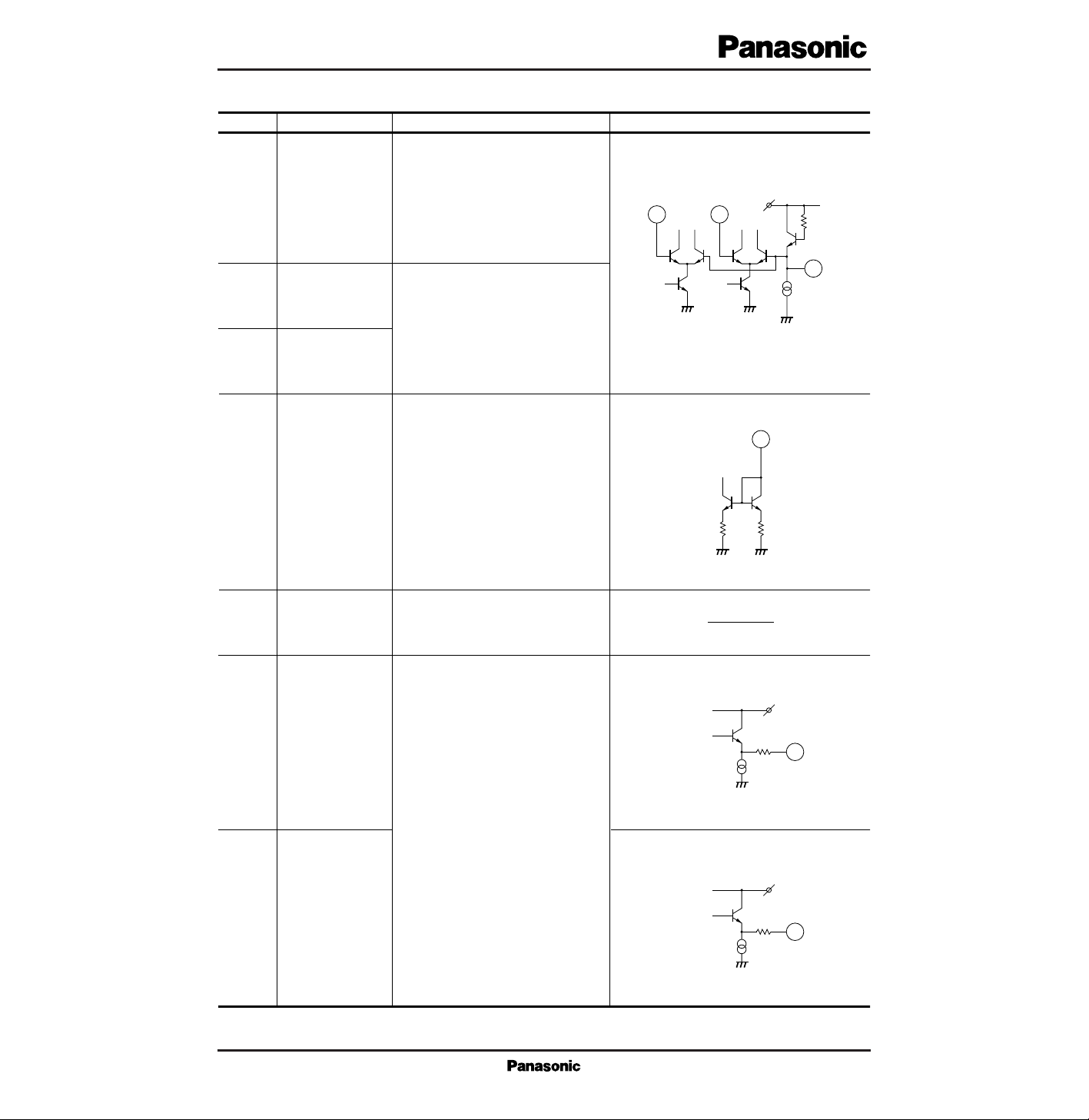
■ Functional Block Diagram
■ Pin Descriptions
Pin No.
Description
1
2
3
4
5
MIX bias
L–OSC input (1)
L–OSC input (2)
MIX current control
V
CC
Pin No.
Description
6
7
8
9
10
MIX (2) output
MIX (1) output
GND
RF bias
RF input
Page 2

Parameter Symbol Rating Unit
■ Absolute Maximum Ratings (Ta=25˚C)
Supply voltage
Supply current
Power dissipation
Operating ambient temperature
Storage temperature
V
CC
I
CC
P
D
T
opr
T
stg
4
20
143.5 (Ta=75˚C)
–20 to + 70
–55 to +125
V
mA
mW
˚C
˚C
Note) Protect pins 3, 9, and 10 from electrostatic discharge.
Parameter Symbol Range
■ Recommented Operating Range
V
CC
1.8 to 3V
Operating supply voltage range
Parameter Symbol Condition min typ max Unit
■ Electrical Characteristics (VCC=2.0V, Ta=25±2˚C)
Current consumption
0.6Itot 1.4 mA1.0
Input Level –54dBm, f=450.0045MHz
MIX output level (1)
–38VMIX1 –30 dBs–34
MIX output level (2)
–38VMIX1 –30 dBs–34
Input Level –54dBm, f=450.0045MHz
Parameter Symbol Condition min typ max Unit
■ Electrical Characteristics (Design Values for Reference) (VCC=2.0V, Ta=25±2˚C)
RF bias voltage
VRF V0.745
MIX bias current
VMIX V1.3
MIX output level difference
–3.2DVmix 3.2 dB
25
dBs
DVmix=Vmix1–Vmix2
The following are design values for reference only (not guaranteed)
Output noise level
Vn3
Vn3=
(Vn2)2 + (Vn2)
2
2
Page 3
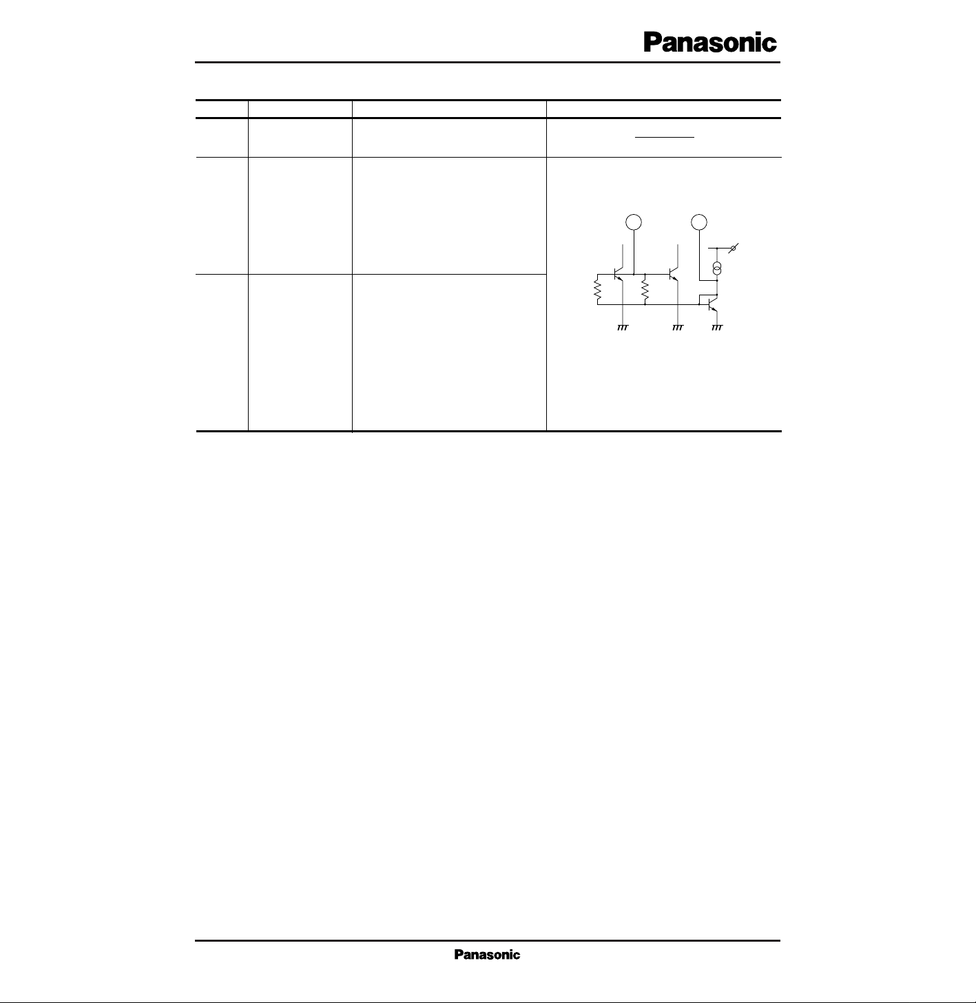
■ Pin Descriptions
Symbol Description Equivalent circuit
1
Local oscillator bias. Normally
grounded though a capacitor.
MIX bias
Pin No.
2
L-OSC input 1
3
L-OSC input 2
Local oscillator inputs to Pin2 w and 3
are different in phase by π/2.
These inputs are different in frequency
by FM Dev from Pin 10 input.
4
MIX-current
control
Current input to this pin controls the
IC's operation and total current. This pin
may be connected to Pin 22 of AN6400.
5
V
CC
This is the supply voltage pin.
Direct-conversion mixer outputs (FM
Dev.).
These outputs are different in phase by
π/2 from each other. These pins may be
to AN6400 or other direct conversion
demodulator ICs for data retrieval.
6
MIX2 output
7
MIX1 output
6
2
V
CC
100Ω
V
CC
7
100Ω
V
CC
4
2.4kΩ
12kΩ
2.4kΩ
3
1
Page 4
Symbol Description Equivalent circuit
9
This is the bias pin for RF input to Pin
10. The bias us internally provided. This
pin must be ground through a capacitor.
RF bias
Pin No.
8 GND
This is the ground pin.
10
FSK-modulated RF signals from an RF
amplifier are input to this pin. RF
signals with up to 450MHz are
acceptable.
RF input
1.2kΩ
10
9
V
CC
1.2kΩ
■ Pin Descriptions (Cont.)
 Loading...