

Page 1
■ Overview
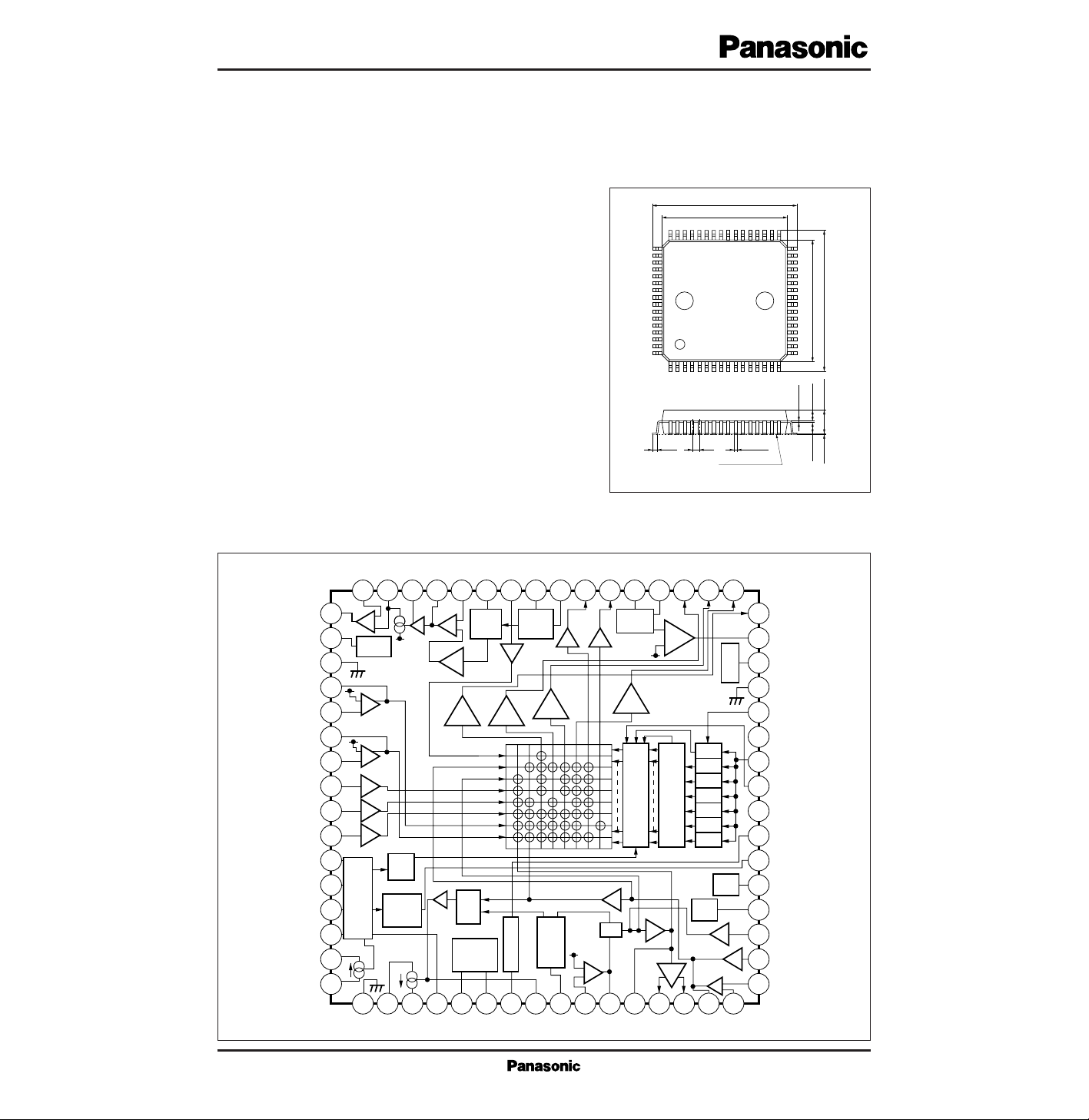
The AN6448NFBP is a speech network IC suitable for multifunction cordless telephones. It incorporates a cross-point
switch controlled by serial input. It allows speech path switching and mixing, and provides for three- or four-person communication and other sophisticated functions. It also incorporates
REC/PLAY amplifiers with VOX circuits.
■ Features
•
The speech block can operate on line voltage, with no external power supply, and is operational even during a commercial power failure.
•
Incorporates auto. PAD, dial mute, DC voltage regulation,
and other basic speech functions.
•
The cross-point switch can be operated independently.
•
Each output of the cross-point switch can correspond to multiple inputs, allowing three-or four-person communication.
•
The REC/PLAY amplifiers incorporate ALC and VOX circuits.
•
Receiver volume can be increased by 6 dB or 9 dB.
AN6448NFBP
Speech Network IC Incorporating Cross-Point Switch
Unit : mm
QFP package with 64 pins (QFH064-P-1414A)
17.2±0.4
14.0±0.3
17.2±0.4
14.0±0.3
48 33
116
17
32
64
49
2.85±0.2
1.3±0.11.3±0.1
0.1±0.1
0.2
+0.1
-0.05
0.35
+0.1
-0.050.8(0.8)
SEATING PLANE
■ Block Diagram
3348 47 46 45 44 43 42 41 40 39 38 37 36 35 34
1
2
3
4
5
6
DC
Cont.
0dB
32
31
I
30
N
J
29
28
27
26
25
24
23
22
21
20
19
0dB
18
–
17
+
49
–
+
50
V
REF
51
52
+
–
53
54
+
–
55
0dB
56
0dB
57
0dB
58
59
P.O.R
–
+
10dB
0/12dB20
ACL
ACL
Det
0dB
dB
0dB 0dB
18
dB
VOX
Det.
18
dB
Latch
Comp
Decoder
D
a
a
a
a
a
a
60
61
62
Line
Supply
Monitor
Power Supply
Control
63
AP
AP
V
REF
Cont.
Hold off
64
0dB
AP
0dB
+
–
DM
Cont.
20
dB
16123456789101112131415
Page 2

V
CC
I
CC
V
L
I
L
P
D
T
opr
T
stg
Supply voltage (1)
Supply current (1)
Supply voltage (2)
Supply current (2)
Power dissipation
Note)
Operating ambient temperature
Storage temperature
V
mA
V
mA
mW
˚C
˚C
■ Absolute Maximum Ratings (Ta=25˚C)
7.0
50
12.0
135
640
–20 to +75
–55 to +150
Note) In a free-air condition with Ta=75˚C.
Parameter Symbol Rating Unit
■ Recommended Operating Conditions (Ta=25˚C)
Operating supply voltage range (1)
Operating supply voltage range (2)
Clock frequency
V
CC
V
L
f
CLK
4.5
3
5 5.5
11
250
V
V
kHz
Parameter Symbol Condition min typ max Unit
■ Electrical Characteristics (Ta=25˚C)
Speech network block
Rec. gain
G
V
–ER1 34.5 dB
IL=30mA, VCC=5V,
Vin=–42dBm
30.5 32.5
Rec. automatic PAD width
AP–ER 5 dB
IL=30 to 80mA, VCC=5V,
Vin=–42dBm
2.5 3.7
Trans. gain
G
V
–EM1 31.7 dB
IL=30mA, VCC=5V,
Vin=–38dBm
27.7 29.7
Trans. automatic PAD width
AP–EM 5 dB
I
L
=30 to 80mA, VCC=5V,
Vin=–38dBm
2.5 4
DTMF gain
GV–ED1 20.9 dB
IL=30mA, VCC=5V,
DM=ON, Vin=–30dBm
I
L
=30 to 80mA, VCC=5V,
V–DMC=LOW,
Vin=–30dBm
16.9 18.9
DTMF automatic PAD width
AP–EDT 5.5 dB2.5 4.1
REC/PLAY amp. block
Switch block
Head bias current
145I–REC µA
180 215
REC preamp. output
–13.4V
O
–RP dBm
Vin=–45dBm, Rin=10kΩ
–11.4 –9.4
EQ amp. gain
27.8G
V
–EQ dB
Vin=–40dBm
29.8 31.8
SP out max output
0V
O
–SP dBm
Input L-SP IN, THD=5%
4
DH out max output
0V
O
–DH dBm
Input RF1 IN, THD=5%
4
RF1 out max output
0V
O
–RF1 dBm
Input RF2 IN, THD=5%
4
RF2 out max output
0V
O
–RF2 dBm
Input RF1 IN, THD=5%
4
L-REC out max output
0V
O
–LR dBm
Input AUX IN, THD=5%
4
Parameter Symbol Condition min typ max Unit
Page 3
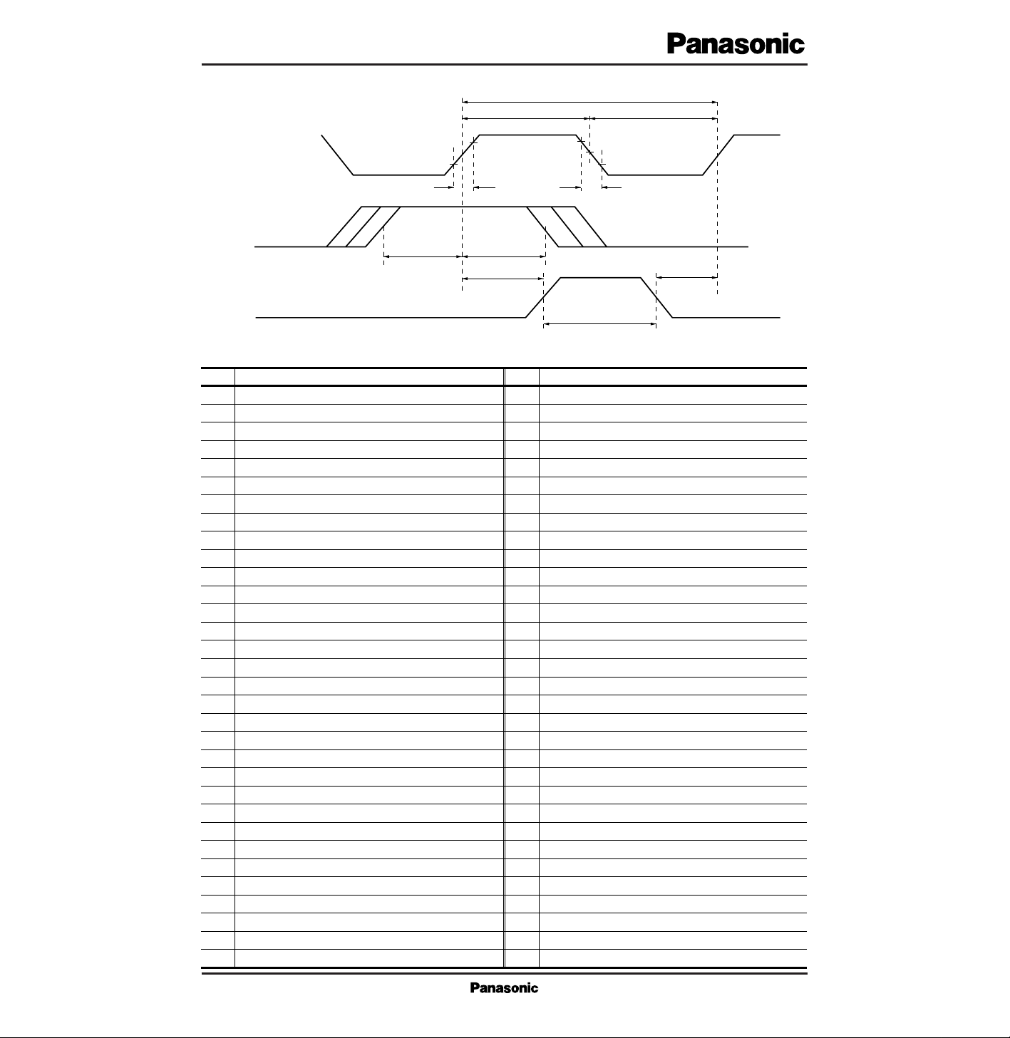
■ Timing Chart
CLK
DATA
STR
1/f
CLK
t
wh (CLK)
90%
10% 10%
2.5V
90%
2.5V
2.5V
2.5V 2.5V
2.5V
2.5V
t
WL (CLK)
t
r (CLK)
t
f (CLK)
t
su (DATA)
t
h (DATA)
t
su (STB)
t
sr (STB)
t
W (STB)
■ Pin Descriptions
Pin No.
Description
1
2
3
4
5
6
7
8
9
10
11
12
13
14
15
16
17
18
19
20
21
22
23
24
25
26
27
28
29
30
31
32
Ground
Line power (+) input
Side-tone adjustment
Line voltage control (1)
Int. ref. voltage output (1)
Int. ref. voltage output (2)
Hold-reset control
Trans. preamp. output
Auto. PAD control
Rec. preamp. input
Rec. preamp. output
Rec. amp. input
Rec. amp. output (1)
Rec. amp. output (2)
MIC preamp. output
MIC preamp. input (1)
MIC preamp. input (2)
DTMF signal input
BT signal input
Dial mute control
Line voltage control
Line interruption detector output
Hold-reset signal output
No connection
Strobe signal input
Clock signal input
No connection
Data input
Ground
Logic power supply input
VOX detector output
SP link output
Pin No.
Description
33
34
35
36
37
38
39
40
41
42
43
44
45
46
47
48
49
50
51
52
53
54
55
56
57
58
59
60
61
62
63
64
RF2 link output
RF1 link output
Intercom link output
VOX detection control
VOX amp. input
Time stamp link output
Recording link output
ALC input
ALC detection control
Loudspeaker link input
Recording input
Recording inverse input
Recording preamp. output
Recording bias current control
To recording head
EQ amp. inverse input
EQ amp. output
REC/PLAY int. ref. voltage output
Ground
MIX preamp. output
MIX link input
AUX preamp. output
AUX link input
Intercom link input
RF1 link input
RF2 link input
Power-ON reset control
External supply voltage input
Internal supply voltage output
Circuit voltage control (2)
Line current bypass (2)
Line current bypass (1)
Page 4

■ Pin Descriptions
1 GND
2 V
L
I
3 ST
V
L
–
CONT
I
O
4
V
REF
–
SN
HCO
HCC
APC
Vreg-R · I
I
L
T–
FILTER
5 V
REF
O
O
O
I
I
O
O
O
6
7
23
8
9
10
RV IN
RV
PRE
–
OUT
RV
FILTER
RV
OUT
(1)
RV
OUT
(2)
11
12
13
·
14
DescriptionWaveform Remarks
PinNo.
Symbol
I/O Equivalent Circuit
TO
2
3
62
7
30kΩ
120kΩ
+
–
+
–
23
4
8
6kΩ
9
IχI
L
I
10
11
+
–
+
–
10kΩ
11
13
14
12
61
5
6
24kΩ
24
kΩ
Vreg
+
–
+
–
0V
DC
3 to 10V
DC
0.3V
DC1V
1V
(Const)
1V
(Const)
I
L
DC1V
V
REF
V
REF
V
REF
V
REF
V
REF
V
CC
0V
Hold-reset signal
Ground :
• This is the ground pin for the
speech network.
GND for REC/PLY, VRER
SPEECH and LINK.
Side-tone adjustment :
• Grounded through R1 (27Ω).
• Connects to the side-tone adjusting circuit to adjust side tone and
receiver level.
Int. ref. voltage output (1) :
• Outputs half the Vreg reference
voltage.
• Grounded through a 0.01µF
capacitor.
Line voltage control (1) :
C
2
and the internal resistance
determine the f. characteristics.
The larger the capacitance
of C10, the lower the high
band gain as with a LPF.
The larger the capacitance of
C
5
, the wider the pulse width.
C6 and the 6-kΩ internal
resistance as illustrated on the
left form a low-pass filter.
The receiver preamplifier
gain (G) is :
The line drive gain (G) is :
Z
Line
//Z
Tel
R
1
Also assuming
Z
Line
600Ω
Z
Tel
600Ω
R1=27Ω :
G=20log =20.9dB
Int. ref. voltage output (2) :
• Output impedance=50Ω
Line power input :
• Connects to the positive output
of the diode bridge.
Hold-reset control :
• Grounded through C5. Adjusts
the output time of control signals.
Hold-reset signal output :
• This is an open-collector output to a microprocessor.
• Requires a pull-up resistor.
Trans. preamp. output :
• C
6
as connected between this pin
and the ground forms a low-pass
filter.
Auto. PAD control :
• Connects through a resistance to
Pin61 (Vreg). If the resistance
increases, the PAD operates
closer to the near end. If the
resistance decreases, the PAD
operates closer to the far end.
Rec. preamp. input :
• Receiver signals are input from
the side-tone circuit to this pin.
• R7 and C8 connected between
Pin11 and this pin determine
Rec. preamp. output :
• R7 and C8 connected between
Pin10 and this pin determine
the f. characteristics.
• The output impedance is 100
±50Ω.
Rec. amp. outputs (1 and 2) :
• A ceramic or dynamic receiver is connected.
• The output circuit is a BTL configuration.
• The output impedance is 50±
30Ω.
Rec. amp. input :
27
300
G= –20log
R7
+ωC8
1
ωC9
R6 +
1
1
G =
Page 5

■ Pin Descriptions (cont.)
15
MIC
OUT
16
O
MIC
IN
(+)
MIC
IN
(–)
I
I
17
18
MF–
IN
BT–
IN
DMC
DC–
CONT
I
I
I
O
I
I
I
19
20
21
22 CPC
NC
STR
CLK
NC
24
25
26
27
MIC preamp. input (1) :
• A bias resistor and a microphone
connect to this pin.
MIC preamp. output :
• R11 and C13 connected
between Pin17 and this pin
determine the f. characteristics.
• The output impedance is 300
±100Ω.
Feedback is input to this pin
through a capacitor. The
capacitor and R9 to R11, and
C12 and C13 determine the f.
characteristics.
The input impedance (10kΩ)
and C14 or C15 form an
input HPF.
• Referring to the left figure, the
voltage, VCPC, at which
T
rCPC
turns ON is calculated
as follows:
V
CPC
(ON)
DTMF signal input :
• DTMF signals are input through
a coupling capacitor C14.
• When DMC is low at Pin20,
DTMF is enabled.
• Input impedance is 10kΩ.
Dial mute control :
• Normal speech mode when Pin20
is high or open (MIC amp. ON
and rec. amp. ON).
• DTMF mode when Pin20 is low
(DTMF amp. ON and BT amp.
ON).
Line voltage control :
• Line voltage is normal when this
pin is high. Line voltage increases by 1 to 1.5V when this pin is
low.
Line interruption detector output :
• This is an open collector output
to a microprocessor, requiring a
pull-up resistor connected to the
microprocessor's power supply.
This pin goes low when line
voltage is 3.0V or more, and
goes high when 1.5V or less.
No connection
No connection
MIC preamp. input (2) :
• R11 and C13 connected
between Pin15 and this pin
determine the f. characteristics.
BT signal input :
• Beep tone (BT) signals are
input through a coupling
capacitor C15.
• Input impedance is 10kΩ.
Strobe signal input :
• The strobe signal for serial control
data is input to this pin. The rising
edge of the strobe signal determines the timing at which internal
control address or ON/OFF status
is validated.
Clock signal input :
•
The clock signal for serial control
data is input to this pin. The rising
edge of the clock signal determines
the timing at which data is
read.
× VBE (T
rCPC
)
=
= 2.5V (Ta=25˚C)
R1 + R2
R1
DescriptionWaveform Remarks
PinNo.
Symbol
I/O Equivalent Circuit
17
16
10kΩ
+
–
V
REF
15
18
10kΩ
V
REF
/SN
19
10kΩ
V
REF
200kΩ
100kΩ
20
61
300kΩ
V
CC
10kΩ
26
200kΩ
150kΩ
21
144kΩ
V
L
R2
R1
56kΩ
22
2
Tr
CPC
300kΩ
V
CC
10kΩ
25
+
–
+
–
+
–
V
REF
V
REF
With signal ON
V
REF
With signal ON
V
REF
V
CC
0.2V
Line voltage increases
V
CC
0.2V
Line interruption
5V
0V
5V
0V
Page 6

28 IDATA
29
30
GND
L –
V
CC
VOX.
OUT
O31
32
SP.
OUT
DH –
OUT
VOX
DET
O
O
O
I
RF2 –
OUT
O33
RF1 –
OUT
O34
35
36
VOX
IN
37
Data input :
• Serial data is input to this pin.
Data is read into the internal
shift register in synchroniza-
tion with clock signals.
Ground :
• This is the ground pin for the
logic circuits.
VOX detector output :
• This is an open collector out-
put.
• This pin goes low when voice
signals are input to Pin37.
Loudspeaker link output :
• This is a link switch output to
an external loudspeaker
amplifier.
• The output amplifier gain is
selectable between 12 and 0dB.
• Output impedance is 50±30Ω.
• Output waveforms are shaped
stable internally (by the threshold
circuit).
When address 2F of the crosspoint switch is OFF, the output
amplifier gain is set to 12 dB.
Logic power supply input :
RF2 link output :
• This is a link switch output.
• Output impedance is 50±30Ω.
Intercom link output :
• This is a link switch output to
a intercom.
• Output impedance is 50±30Ω.
VOX detection control :
• A smoothing capacitor (C17) and a
resistor (R19) connect in parallel to
this pin to adjust the attack and
recovery times of the VOX detector.
VOX amp. input :
• VOX (voice detection) signals are
input to this pin.
• Input impedance is 500Ω.
• VOX detection can be done
in two ways :
A) With small C17 (560pF)
and small R19 (39kΩ)
VOX input
VOX output
B) With large C17 (22µF)
and large R19 (100kΩ)
VOX input
VOX output
• Input sensitivity is calculated as follows :
Adjust the f. characteristics
and sensitivity based on the
above calculation.
G =
R2//ZC1
R1
DescriptionWaveform Remarks
PinNo.
Symbol
I/O Equivalent Circuit
RF1 link output :
• This is a link switch output.
• Output impedance is 50±30Ω.
300kΩ
V
CC
10kΩ
28
31
68kΩ
10kΩ
50kΩ
33
34
V
REF
32
30kΩ
10kΩ
50kΩ
LINK
From LINK SW
LINK
From LINK SW
0/12dB
V
REF
V
REF
90kΩ
10kΩ
50kΩ
LINK
From LINK SW
V
REF
35
500Ω
500Ω
R1
R2C1
36
37
V
REF
5V
0V
V
CC
0V
Voice on
V
REF
V
REF
V
REF
V
REF
Half-wave rectification
(with no capacitor)
DC (with a capacitor)
Pin36
output
Pin37 input
+
–
+
–
+
–
+
–
■ Pin Descriptions (cont.)
Page 7

40
ALC.
IN
I
41
ALC.
DET
O
42
SP –
IN
I
43RDPRE –INI
44
RD
PRE –
NF
I
45
REC
PRE –
OUT
O
46
BIAS
ADJ
48
EQ.
NF
I
49
EQ.
OUT
O
50
V
REF
–
PR
O
47
HEAD
I/O
ALC input :
• Pin45 connects through a coupling capacitor to this pin.
• Input impedance is 10kΩ.
• Ground Pin41 if no ALC circuit is used.
• The larger C20, the longer the
attack time. The smaller R22,
the shorter the recovery time.
• Address 07 of the cross-point
SW determines the ON/OFF
status of the rec. preamp.
• The bias current to the head
is :
I
H
= × 3
V
ref
= V
REG
• The gain of the equalizer amp.
is calculated the same way as
the receiver preamp.
• Address 0F of the cross-point
SW determines the ON/OFF
status of the EQ amp.
The gain (G) of the recording
preamplifier is :
G = –
ALC detection control :
• A smoothing capacitor (C20) and a
resistor (R22) connect in parallel to
this pin to adjust the attack and
recovery times of the ALC.
Loudspeaker link input :
• SP signals to this pin are output
through a coupling capacitor to
the link switch.
• Input impedance is 50kΩ.
Recording input :
• Recording signals are input
through a coupling capacitor
to this pin.
• Input impedance is normally 10
kΩ. It decreases during ALC
operation.
Recording preamp. inverse input :
•
A C/R combination between Pin45 and
this pin determines the gain and f. characteristics of the recording preamplifi
er.
Recording preamp. output :
• Outputs amplified recording signals.
• Output impedance is 50±30Ω.
To recording head :
• A recording head connects to
this pin.
EQ amp. inverse input :
• A C/R combination between
pin49 and this pin determines
the equalizer characteristics.
EQ amp. output :
• Outputs amplified equalizer signals.
• Output impedance is 50±30Ω.
REC/PLAY int. ref. voltage
output :
• The pin5 ref. voltage is buffered and output from this
pin.
Recording bias current control :
•
A C/R combination connected to this pin
determines the recording bias current and
gain of a recording head.
•
The smaller the resistance of the C/R combination, the greater the bias current and gain.
R26
R24 +
1
ωC23
Vref
R27
1
2
Full-wave
rectification
(with no capacitor)
V
REF
V
REF
V
REF
V
REF
V
REF
During recording
During playing
Bias voltage
0V
0V
V
REF
V
REF
V
REF
(CONST)
2kΩ
V
CC
40
41
V
REF
LINK
To LINK SW
50kΩ
42
V
REF
From ALC
22kΩ
10kΩ
10kΩ
V
REF
43
44
45
V
CC
R27
45
61
47
46
From recording
head
48
49
V
REF
50
5
V
REF
O
O
LTS –
OUT
LRC –
OUT
38
39
Time stamp link output :
• This is a buffered link switch
output.
• Output impedance is 50±30Ω.
DescriptionWaveform Remarks
PinNo.
Symbol
I/O Equivalent Circuit
Recording link output :
• This is a buffered link switch
output.
• Output impedance is 50±30Ω.
1
2
38
39
V
REF
V
REF
DC (with a capacitor)
Pin$1
output
Input
LINK
To LINK SW
+
–
+
–
+
–
+
–
+
–
+
–
+
–
+
–
■ Pin Descriptions (cont.)
Page 8

■ Pin Descriptions (cont.)
54
55
AUX
OUT
O
AUX
IN
DH IN I
I
56
57
RF1
IN
RF2
IN
PR
V
CC
V
reg
I
I
I
O
58
59
60
61
62 VLC
Internal supply voltage output :
• A power supply derived from line
voltage is output from this pin to
the internal speech network.
Circuit voltage control (2) :
• This pin is grounded through
C38.
2-5 VDC
depending on V
L
The gain of the AUX preamp.
is calculated the same way as
the rec. preamp.
The input impedance as illustrated left and C33, C34, or
C35 form a HPF.
• The larger C36, the longer the
power-ON reset time.
• The power-ON reset signal is output when the supply voltage
reaches 4V.
C38 (typically 47µF) determines how the circuit voltage
fluctuates.
RF2 link input :
• RF1 signals are input through
a coupling capacitor C34 to
this pin.
• Input impedance is 10kΩ.
Power-ON reset control :
• C36 between this pin and GND
determines the power-ON reset
time of the logic circuits.
AUX link input :
• AUX signals are input through a
coupling capacitor to this pin.
External supply voltage input :
• 5 ± 0.5 V power supply is input to
this pin.
55
To LINK SW
54
V
REF
V
REF
V
REF
V
REF
10kΩ
To LINK SW
56
V
REF
V
REF
57/58
10kΩ
To LINK SW
V
REF
V
CC
Reset signal
50kΩ
150kΩ
+
–
59
Comparator
5V
±0.5V
DC
V
CC
– 0.2V
2V during power failure
V
L
2
61
62
64
63
2
52
MIX
OUT
O
53
MIX
IN
I
The gain of the MIX preamp.
is calculated the same way as
the rec. preamp.
MIX preamp. output :
• A C/R combination between Pin53
and this pin determines the gain and
f. characteristics of the MIX preamp.
• Output impedance is 50±30Ω.
MIX link input :
• MIX signals are input through
a coupling capacitor to this pin.
AUX preamp. output :
• A C/R combination between Pin55
and this pin determines the gain and
f. characteristics of the AUX preamp.
• Output impedance is 50±30Ω.
Intercom link input :
• Intercom signals are input through
a coupling capacitor C33 to this
pin.
• Input impedance is 10kΩ.
RF1 link input :
• RF1 signals are input through
a coupling capacitor C34 to
this pin.
• Input impedance is 10kΩ.
V
REF
53
To LINK SW
52
V
REF
51 GND
Ground :
• Output impedance is 50±30Ω.
DescriptionWaveform Remarks
PinNo.
Symbol
I/O Equivalent Circuit
+
–
+
–
+
–
+
–
Page 9

■ Logic Specifications
(Basic Block Diagrams)
Latch circuit
Output (cross-point SW and other controls)
Decoder
(6 bit, 48 channels)
A6 A5 A4 A3 A2 A1
Clock
Clock
Data
Strobe
Data Strobe
D
(A6) (A5) (A4) (A3) (A2) (A1) (D)
1 0 0 1 1 0 1
Reset
Decoder
Shift register
Time charts (assuming the address h26 latch is to be set)
1. Data is read into the shift register in synchronization with a
rising edge of the clock, with the higher data being shifted
sequentially on a first-come highest-bit basis.
2. When the strobe is low, data is shifted sequentially on the
sift register in synchronization with the clock. Data on the
latch circuit will not change.
3. When the strobe goes high, the latched data whose address
is represented by the highest 6-bit of the shift register is
updated. Latched data is set when the least significant bit is
1, and reset when the bit is 0.
4. Referring to 3 above, if the address is h00 (the highest 6bit of the shift register are all 0s), the latch circuit is
cleared (all reset) regardless of the data content.
5. At power-on, the latch circuit is cleared (by power-ON reset).
■ Pin Descriptions (cont.)
I
O
PD2
PDI
63
64
0 to 3V depending
on V
L
Same as above
VL– 33Ω × I
L
Z
Tel
is 1.5 to 2kΩ on the IC
side. It must be adjusted to
600Ω by inserting a 820Ω
resistor between V
L
and GND.
DC
DC
V
L
33Ω
15Ω
64
63
2
Power supply
33Ω
820Ω
R40
100µ
64
V
L
Line current bypass (2) :
• Line current is bypassed from
this pin through R39 to GND.
R39 must be 1/2 W or more.
Line current bypass (1) :
• Line current is bypassed from
this pin through R40 to Pinw.
R40 must be 1/2 W or more.
DescriptionWaveform Remarks
PinNo.
Symbol
I/O Equivalent Circuit
Page 10

2. Other control switches
(Address) (Description)
00 All reset
07 Recording amp. ON
0F Playing amp. ON
17 Receiver volume 6 dB up
1F Receiver volume 9 dB up (when address 17 is on)
27 Handset receiver amp. mute
2F Loudspeaker amp. gain 12 dB down
Note) Address is in hexadecimal.
Note) Empty space means “not applicable.” Address is in hexadecimal.
Input
Output
Line outputHandset rec. Loudspeaker Intercom RF1 RF2 Recording Time stamp
■ Logic Circuits Address Specifications
1. Cross-point switch
Loudspeaker
Microphone
Receiver
Intercom
RF1
RF2
MIX
AUX
10
18
20
28
30
38
09
21
29
31
39
02
0A
12
1A
32
3A
0B
23
2B
33
3B
0C
14
1C
2C
34
3C
0D
15
1D
25
35
3D
0E
16
1E
26
2E
3E
37
■ Package power dissipation
0
200
0 150125100
900mW
Ambient Temperature Ta (˚C)
640mW
Power Dissipation P
D
(mW)
755025
1600
1400
1200
1000
800
600
400
PD – Ta
Page 11

■ Application Circuit
49
50
51
52
53
54
55
56
57
58
59
60
61
62
63
64
32
31
30
29
28
27
26
25
24
23
22
21
20
19
18
17
161 2 3 4 5 6 7 8 9 10 11 12 13 14 15
3348 47 46 45 44 43 42 41 40 39 38 37 36 35 34
10dB
0/12
dB
20
dB
18
dB
18
dB
COMP
+
–
0dB
0dB
0dB
0dB 0dB
0dB
0dB
0dB
0dB
0dB
Vref
VOX
Det.
I
N
J
ALC
Det
ALC
P.O.R
Vref
A P
Line
Supply
A P
A P
Cont.
DM
Cont.
DC
Cont.
D
a
1
a
2
a
3
a
4
a
5
a
6
+
–
+
–
+
–
–
+
–
+
20
dB
RF2. OUT
RF1. OUT
DH. OUT
VOX.
DET
VOX. IN
TS. OUT
ALC. IN
REC. IN
REC.
PRE. NF
REC. PRE. OUT
REC.
ADJ
P.R. HEAD
EQ. IN
ALC.
DET
LINK. REC. OUT
JP30.068µF
0.068µF
0.15µF
22µF
0.47µF
0.1µF
C17
560pF
0.033µF
10kΩ
10kΩ
C18
C19
C20
22µF
R21
R23
100kΩ
10kΩ
10kΩ
1kΩ
56kΩ
R24
C21
C23
C24R25
R27
R26 47kΩ
R26
C25
12kΩ
J4
C22
R19
R20
VOX IN
JP2
LINK R– OUT
ALC IN
LINK SP– IN
PLAY IN
REC OUT
EQ. OUT
C42
22µF
0.01µF
100µF
C28
P/R. V
REF
P/R. GND
MIX. IN
AUX. IN
DH. IN
RF1. IN
(R36 to 38 : for level adjustment)
RF2. IN
AUX. OUT
MIX. OUT
0.068µF
0.068µF
0.068µF
R33
R35
R38
10kΩ
10kΩ
C30
C32
C33
0.068µF
R37
C34
0.068µF
10µF
100µF
PRC
R38
C35
C36
C39
100µF
47µF
100
µF
R4
2.7kΩ
R5
121kΩ
J1
JP1
C1
0.022µF
R3 4.7kΩ
Side-tone circuit
+
–
820kΩ
C37
C38
R15
R33
C39
R40
V
L
VCC
V
REG
VLC
PD2
PD1
GND
GND
V
L
R1 27
22µF
C2
0.01µF
C3
100µF
C4
22µF
0.01µF
0.1µF
0.068µF
0.0015µF
0.068µF
C12
0.068µF
MIC
10kΩ
0.001µF
0.1µF
C11
C8
R7
47kΩ
R8 6.8kΩ
C5
C6
C7
12kΩ
R6
C9
R2 470
ST
V
L
. CONT
Vref1
Vref2
HCO
APC
T. FILTER
R. FILTER
R. PreOUT
R– OUT (1)
R– OUT (2)
10kΩ
27kΩ
R9
R11
C13
C14
0.068µF
C15
R13
CPC
HCC
STR
CLK
DATA
LOGIC. GND
LOGIC. V
CC
VOX. OUT
SP. OUT
C16
NC
NC
SW2
Open
V
REG
10kΩ
R10
MIC. OUT
MIC. IN
MIC. IN (–)
MIC. IN (+)
DYMF. IN
BT. IN
DM. CONT
DC. CONT
R.
PreIN
20kΩ
R32
20kΩ
R34
C26
R29
R30
C27
R31
1kΩ
330kΩ
10kΩ
1µF
+ + +
J3
100µF
120kΩ
R43
SP
SP
LIN REC OUT
TS OUT
Latch
Power Supply Control
Hold off
Decoder
MIC
LIN
DH
DH
RF1
RF2
RF1
RF2
MIX
AUX
To test the circuit, short R41 and
use a 1kΩ resistor for a head.
 Loading...