Page 1

AN-643
APPLICATION NOTE
One Technology Way • P.O. Box 9106 • Norwood, MA 02062-9106 • Tel: 781/329-4700 • Fax: 781/326-8703 • www.analog.com
Closed-Loop Control Circuit Implementation of the ADuC832 MicroConverter® IC
and the AD8305 Logarithmic Converter in a Digital Variable Optical Attenuator
By Mark Malaeb
INTRODUCTION
Today’s optical market may not seem very promising; this
could be due mainly to the cyclical nature of the optical
networking infrastructure. However, the major advancements of the recent past in the optical space cannot be
ignored. Such advancements allowed for complete signal processing in the optical domain without the need to
convert to the electrical domain. Also, because of its wide
bandwidth and high density (DWDM) capabilities, optical
fi ber continues to be and will remain the medium of choice
for data, voice, and video transport. The need to support
such a medium was the reason behind the birth of countless optical devices. Optical attenuators, optical amplifi ers
(EDFA and Raman), laser diode drivers, and photodetectors
are among these devices, just to name a few.
This application note focuses on the control circuitry,
using the ADuC832 MicroConverter IC and the AD8305
logarithmic converter, for a MEMS based, silicon, optical
INTEGRATED
INPUT OUTPUT
COUPLER
SILICON VOA 40dB
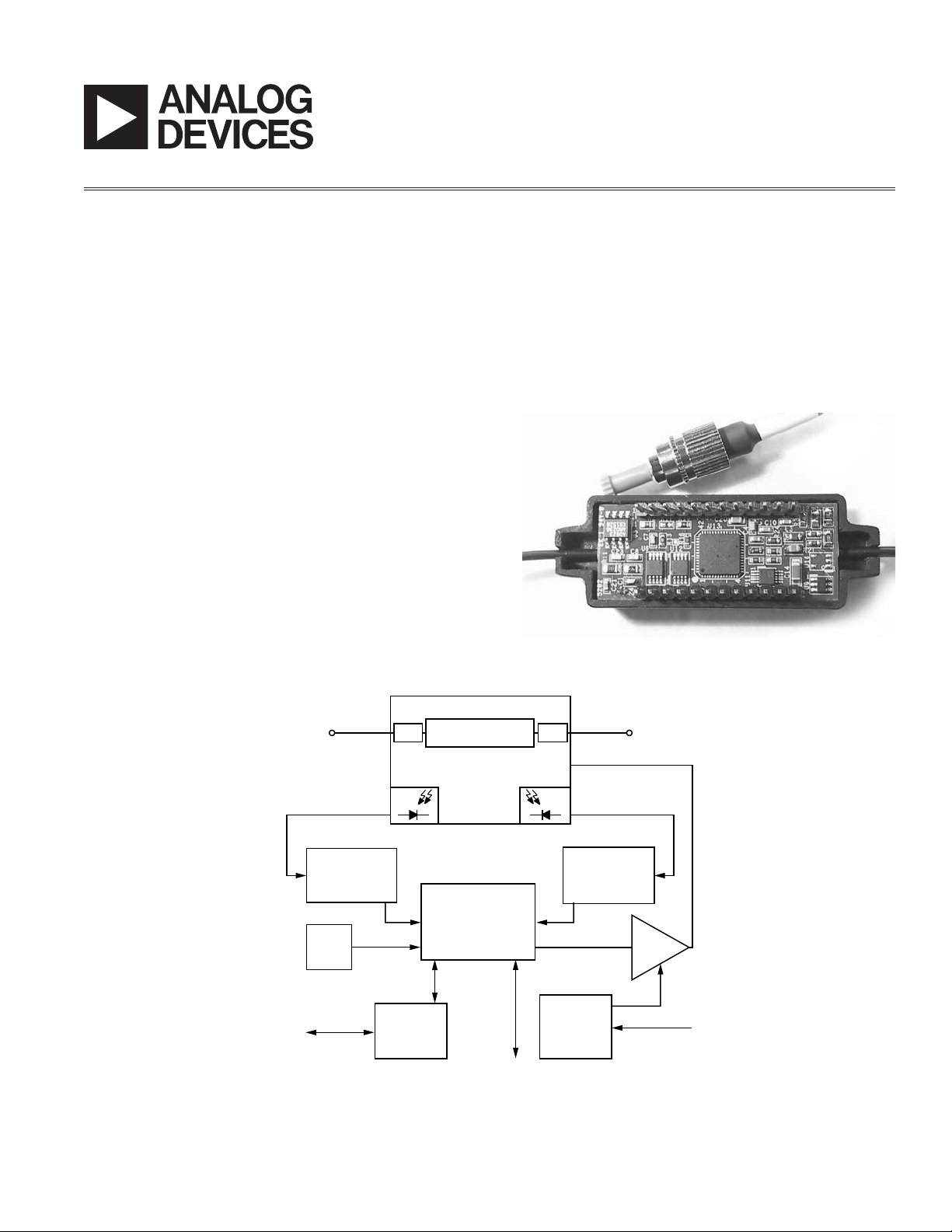
wave-guide, digitally controlled variable optical attenuator (DVOA). Figure 1 shows the physical layout of such a
module, the DVOA by GalayOr, Inc. Figure 2 shows how
the control circuit is implemented in the DVOA module.
Figure 1. GalayOr DVOA
INTEGRATED
COUPLER
INTEGRATED
OPTICAL INPUT POWER
MEASUREMENT
LOG AMP
AD8305
VOLTAG E
REF.
AD1584
RS-232 BUS
RS-232
INTERFACE
ADM101
PHOTODIODES
MicroConverter
ADC1 ADC2
Figure 2. Overall DVOA Module Block Diagram
REV. 0
Purchase of licensed I2C components of Analog Devices or one
of its sublicensed Associated Companies conveys a license for
the purchaser under the Philips I
components in an I
forms to the I
2
C system, provided that the system con-
2
C Standard Specifi cation as defi ned by Philips.
2
C Patent Rights to use these
ADuC832
ATTENUATOR
DAC1
CONTROL VOLTAGE
C/SPI BUS
BOOSTER
2
I
OPTICAL INPUT POWER
MEASUREMENT
LOG AMP
AD8305
36V
VOLTAG E
CIRCUIT
AD823
5V
Page 2

AN-643
SYSTEM FUNCTIONAL DESCRIPTION
This DVOA is designed to attenuate optical signals up to
40 dB. The input and output optical power is measured
using two integrated (1%) optical couplers and their corresponding photodiodes. The output currents from the
photodiodes are fed into the log amps. The log amps
convert the photodiode currents into a voltage proportional to the optical signal power level. These two vol tages
are then fed into two different ADC channels, on board
the MicroConverter IC, for processing.
Once the VOA input and output power levels are known,
an attenuation value is derived from the difference. The
VOA attenuation value is set using an analog control voltage in the range of 5 V to 26 V. The attenuation increases
with increasing voltage levels. This control voltage is
generated from the DAC on board the MicroConverter IC.
The voltage at the DAC output is amplifi ed to the 5 V to
26 V levels using one of Analog Devices’ high voltage op
amps (AD823). A voltage booster, from 5 V to 36 V, is used
to bias the AD823. Also, a high precision voltage reference
(AD1584) is used by the ADC and DAC.
In the following paragraphs, a detailed description of the
functions and features of the control loop’s main components is presented.
ADuC832 MicroConverter IC
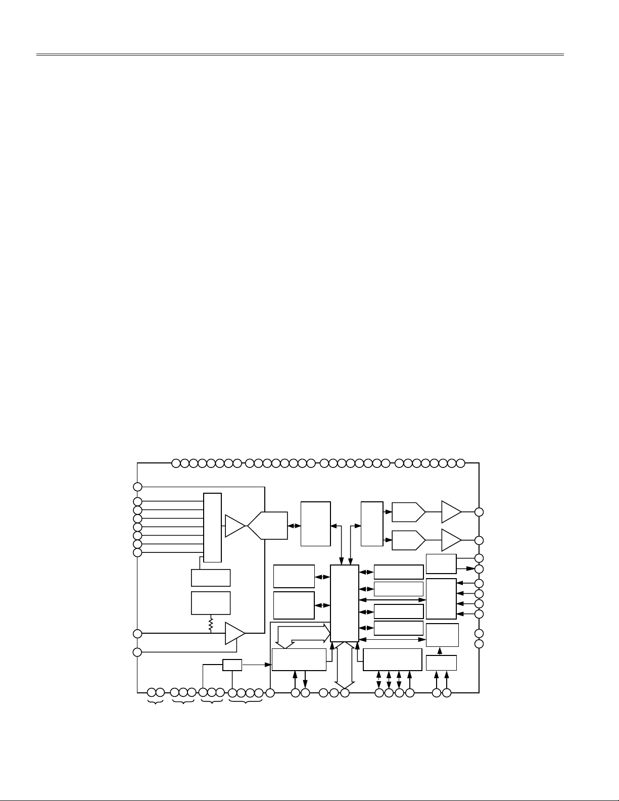
The ADuC832 MicroConverter IC, shown in Figure 3, is
part of an 8052 based ADuC8xx controller family from
Analog Devices. As shown in Figure 3, the MicroConverter
IC integrates an 8-channel multiplexed 12-bit SAR analogto-digital converter and two 12-bit digital-to-analog
converters. Two channels are used to measure the output
voltages from the AD8305 log amps, which correspond
to the optical power levels present at the input and output
of the VOA. One of the two on-board DACs is used to put
out a voltage signal level proportional to the difference
between the DVOA input and output ADC readings.
The MicroConverter IC control circuitry consists of an 8052
core with 62 Kbytes of program memory and 4 Kbytes
of data memory. The preset VOA attenuation numbers,
which are used to set the DAC, are stored in data memory.
Two PWM outputs are also available on board in addition
to the standard timers. To add to this high level of integration, the ADuC832 and all the ADuC8xx family include an
on-board power-on reset circuit, a voltage reference, a
temperature sensor, and a phase-locked loop (PLL). The
PLL makes it possible to run the core with a small and
inexpensive industry-standard 32 kHz watch crystal.
All these features plus all the standard peripherals that come
with an 8052 based controller, i.e., RS-232 interface and
2C®
I
/SPI®, are integrated in a 56-lead LFCSP space-saving
package. This will make a perfect fi t in the housing of this
47 mm 17 mm 10 mm DVOA module.
HARDWARE
CONVST
ADC0
ADC1
ADC2
ADC3
ADC4
ADC5
ADC6
V
REF
C
REF
P0.0
P0.1
P0.2
P0.3
P0.4
P0.5
P0.6
P0.7
P1.0
P1.1
P1.2
P1.3
P1.4
P1.5
P1.6
P1.7
P2.0
P2.1
P2.2
P2.3
P2.4
P2.5
P2.6
P2.7
P3.0
P3.1
P3.2
P3.3
P3.4
P3.5
P3.6
BUF
BUF
PWM
16-BIT
COUNTER
TIME
OSC
34
XTAL1
P3.7
TIMERS
35
XTAL2
11
12
41
42
24
25
56
20
21
1
DAC0
DAC1
PWM0
PWM1
T0
T1
T2
T2EX
INT0
INT1
2
3
47
46
25
56
1
2
3
13
14
15
10
9
5
6
4
DD
AV
48
49
MUX
TEMP
SENSOR
2.5V
BAND GAP
REFERENCE
7
8
223651
AGND
525354
AIN
DD
DV
T/H
BUF
POR
55
56
12-BIT ADC
(–3mV/C)
233738
DGND
1
131415
4K 8
DATA
FLASH/EE
62K 8
PROGRAM
FLASH/EE
DOWNLOADER
DEBUGGER
ASYNCHRONOUS
SERIAL PORT
(UART)
50
17
RESET
18
RxD
ADC
19
TxD
16
AND
CONTROL
3031323339
ADuC832
CALIBRATION
8052
MCU
PORE
EMULATOR
SINGLE-PIN
45
44
43
EA
ALE
PSEN
4041421819202124252627
DAC0
DAC
CONTROL
DAC1
2K 8
USER XRAM
256 8
USER RAM
WATCHDOG
TIMER
POWER SUPPLY
MONITOR
SYNCHRONOUS
SERIAL INTERFA CE
(SPI)
282921
MOSI
SCLOCK
MISO
14
SS
INTERVAL
COUNTER
AND PLL
Figure 3. ADuC832 MicroConverter Block Diagram
–2–
REV. 0
Page 3

AN-643
AD8305 LOGARITHMIC AMP
The AD8305 logarithmic converter belongs to an Analog
Devices family of converters optimized for converting
optical power, measured as electrical current from a
photo diode, into a voltage level. The AD8305’s operation
is based on a translinear technique to provide a wide
dynamic range of power measurements (over five
decades) . The input current, from a photodiode, is applied
to the collector of an NPN transistor, which in turn converts this current into a voltage (V
). The VBE voltage is
BE
directly propor tional to the logarithm of the input current
establishing the basic logarithmic relationship. A second
identical NPN transistor is used to generate a second V
BE
to use as a fi xed refer ence for the co nverter. The dif ference
of the transistor V
provides an absolute measurement
BE
of the photodiode current and provides an output logvoltage that is proportional to the dB equivalent of the
incident optical power.
Temperature compensation circuitry is employed to ensure
good log conformity to within 0.1 dB over a wide range
of temperatures. The device is designed to operate with
a single positive supply. However, it can be run with dual
supplies. This feature provides fl exibility, especially where
the anode on the photodiode has to be at the ground
level. A functional block diagram of the AD8305 is shown
in Figure 4.
The AD8305 includes an on-board amp to be used as a
buffer or for amplifi cation as required by the specifi c
application. All these features are packaged in a spacesaving 16-lead 3 mm 3 mm LFCSP package. For more
details on the AD8305, refer to its data sheet.
Two such log amps are implemented in the previously
described DVOA. One is used to measure the current
from the input photodiode and the other to measure the
output. (A dual version of the AD8305 will be offered in
the near future.) Through the use of the ADC on board the
MicroConverter IC, these measurements are compared
and processed to provide the corresponding digital value
to the on-board DAC.
Communication, for calibration purposes, with the DVOA
module is done through the serial communication port
using the ADM101 from ADI. Communication is also done
choice for optical module designs.
over the I
2
C bus, which seems to have become the preferred
These days, component suppliers must focus on simple
and low cost optical components to be integrated in
existing systems, resulting in short- term revenues. The
Var iab le Op tic al A tt enu ato r (VOA ) is one of the most basic
but essential optical building blocks in the evolution of
optical net works. It exist s in m o s t o p t i c a l s u b s y s t e m s a n d
applications, such as optical amplifi ers, optical add/drop
modules, equalization modules, and testing elements.
With its various applications and growing use in optical
networking, the VOA component market is showing impressive growth and is expec ted to reach sales revenues of
$400M to $600M in 2006 (KMI/RHK). With this promising
VOA market forecast, Analog Devices is well positioned
to supply the electronic control circuitry needed to support such a module.
REV. 0
V
BIAS
200k⍀
1k⍀
1nF
PD
1k⍀
1nF 1nF
5V
VPOS
VRDZ
VREF
IREF
INPTI
VSUM
0.5V
0.5V
20k⍀
80k⍀
COMM
Q2
Q1
VNEG
GENERATOR
2.5V
V
BE2
COMPENSATION
V
BE1
BIAS
TEMPERATURE
Figure 4. AD8305 Log Amp Block Diagram
–3–
14.2k⍀
6.69k⍀
COMM
I
LOG
COMM
451⍀
VOUT
SCAL
BFIN
0.2 log
I
PD
()
10
1nA
Page 4

E03644–.1–3/03(0)
© 2003 Analog Devices, Inc. All rights reserved. Trademarks and registered trademarks are the property of their respective companies.
–4–
 Loading...