

Page 1
■ Overview
The AN6167S and AN6167SB are speech network ICs for
the handset of a cordless telephone. They incorporate compander, MIC, and receiver amplifiers. With a minimal number of
external components, they can perform all the functions of the
handset of a cordless telephone featuring low radio-transmission noise.
■ Features
•
The compressor/expander circuit incorporates preamplifiers
to make level and frequency adjustments easier.
•
The standby circuit provides for a low-power consumption
cordless telephone.
•
The expander has a 6-dB amplifier to allow received-signal
amplificaition.
•
SOP package with 1.27mm pitch pins, and USO package
with 0.8mm pitch pins.
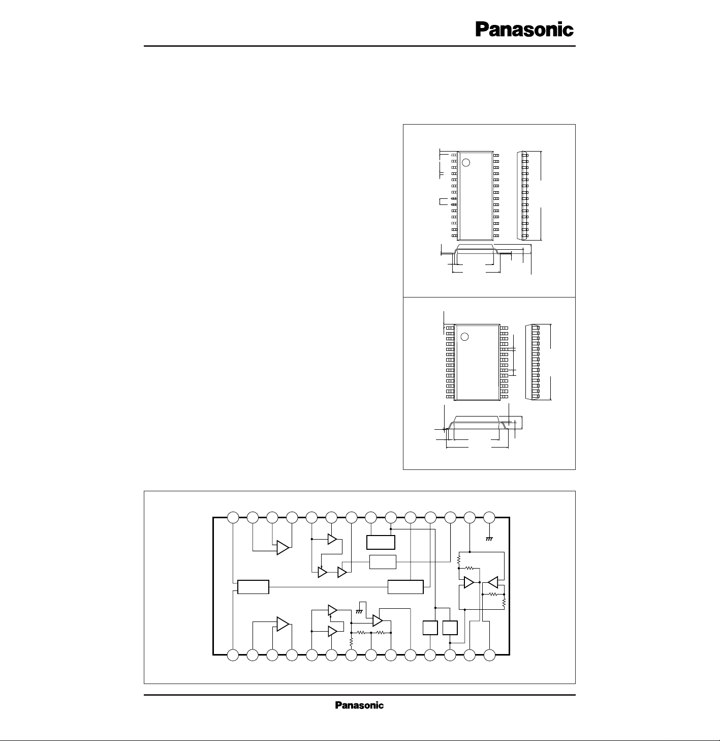
AN6167S, AN6167SB
Cordless Telephone Speech Network IC
Unit : mm
AN6167S
SOP package with 28 pins (SOP028-P-0375A)
1
2
3
4
5
6
7
10
11
12
13
14
8
9
28
27
26
25
24
23
22
21
20
19
18
17
16
15
0.45
0.4±0.25
1.27
17.81±0.3
0.1±0.1
2.0±0.2
0.925
0.15
0.3
7.2±0.3
9.4±0.3
■ Block Diagram
Unit : mm
AN6167SB
SSOP package with 28 pins (SSOP028-P-0375)
1
14
28
15
(0.45)
11.6±0.3
0.3±0.1
0.8
2.0±0.2
0.1±0.1
0.9
0.15
0.3
7.2±0.3
9.3±0.3
VCCEPIE
28 27 26 25 24 23 22 21 20 19 18 17 16 15
1
GNDC
POWER
2
C
PICPNCPOCCCACDETCINCORCOUT
EPOE
PN
–
+
+
–
3 4 5 6 7 8
CCAEDETEOUTEREFVREF
DET
E
CCA
CCA
C
DET
STC STBV DG
VR
E
D6dB
STBY
+
–
9 10 11 12 13 14
VR
C
C
C
REF
PC
R
IN
–
+
REC
VR
R
R
REFRO –2RO –1
GNDG
REC
+
–
Page 2
V
CC
V
in
V
out
P
D
T
opr
T
stg
Supply voltage
Input supply voltage
Output supply voltage
Power dissipation (Ta = 75˚C)
Operating ambient temperature
Storage temperature
V
V
V
mW
˚C
˚C
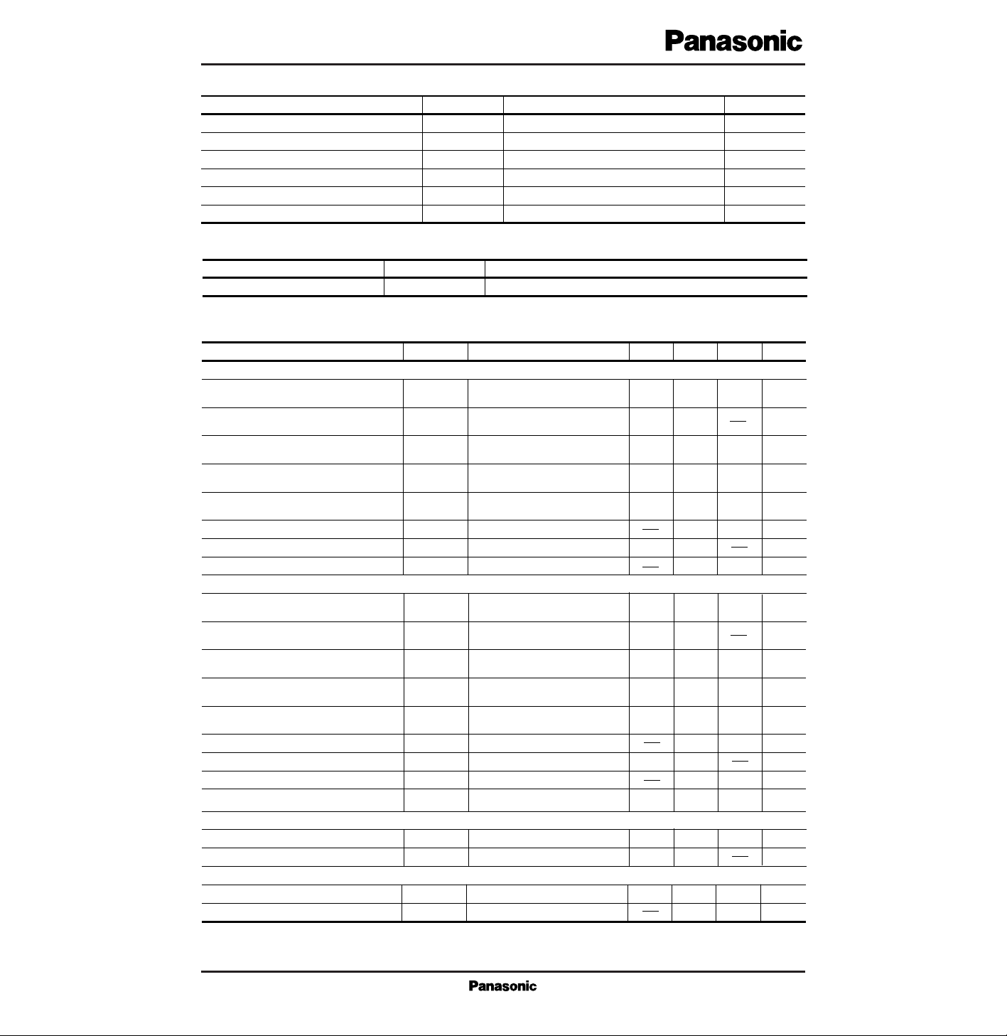
Parameter Symbol Rating Unit
■ Absolute Maximum Ratings (Ta=25˚C)
7.5
– 0.3 to V
CC
+ 0.3
– 0.3 to V
CC
+ 0.3
280
–20 to + 75
–55 to +150
Parameter Symbol Range
■ Recommended Operating Range (Ta=25˚C)
Operating supply voltage range
V
CC
2 to 5V
Parameter Symbol Condition min typ max Unit
■ Electrical Characteristics (Ta=25˚C)
Compressor
Expander
Preamplifier voltage gain
G
PC
22 dB
RA/RB=51kΩ/5.1kΩ,
V
in
=–40dBV
20 21
Preamplifier output voltage
V
PC
dBV
RA/RB=51kΩ/5.1kΩ,
THD=5%, R
L
=1kΩ
–10 –7
Maximum output voltage
–10V
OCM
dBV
Output noise voltage V
NOC
dBV
Receiver amplifier
Distortion
THD
C
Vin=–20dBV
THD=5%, RL=1kΩ
Rg=2kΩ
with a CCITT filter
0.5
–7
1 %
–56–64
Reference output
V
ORC
–9 dBV
V
IRC
=–20dBV
(Ref. output)
–13 –11
∆ Gain (1)
∆C
1
–9 dB
Vin=V
IRC
–20dB,
∆C
1=VORC–VOC1
–11 –10
Preamplifier voltage gain
G
PE
22 dB
RA/RB=51kΩ/5.1kΩ,
V
in
=–40dBV
20 21
Preamplifier output voltage
G
PE
dBV
RA/RB=51kΩ/5.1kΩ,
THD=5%, R
L
=1kΩ
–10 –7
Reference output
V
ORE
–26 dBV
V
IRE
=–20dBV
(Ref. output)
–32 –29
∆ Gain (1)
∆E
1
–19 dB
Vin=V
IRC
–10dB,
∆E
1=VORE–VOE1
–21 –20
∆ Gain (2)
∆E
2
–38.5 dB
Vin=V
IRC
–20dB,
∆E
2=VORE–VOE2
–41.5 –40
∆ Gain (2)
∆C
2
–19 dB
Vin=V
IRC
–40dB,
∆C
2=VORC–VOC2
–22 –20
Receiver amp. gain
∆G
E
Pin17 ON [GND]
4 6 8 dB
Maximum output voltage
–10V
OFM
dBV
Output noise voltage V
NOE
dBV
Distortion
THD
E
Vin=–20dBV
THD=5%, RL=1kΩ
Rg=2kΩ
with a CCITT filter
0.5
–7
1 %
–90–95
Power supply
Receiver voltage characteristics
G
VR
Vin=–30dB, RL=1kΩ
18 20 22 dB
Current consumption
I
CC
VCC=3V, no signal
3 5 8 mA
Receiver voltage characteristics
I
SC
Standby pin (H)
1 10 µA
Maximum output voltage
V
OEM
THD=5%, RL=1kΩ
2 5 dBV
Page 3

■ Pin Descriptions
Pin No.
DescriptionSymbol
1
2
3
4
5
6
7
8
9
10
11
12
13
14
GNDC
C
PI
C
PN
C
PO
C
CCA
C
DET
C
IN
C
OR
C
OUT
C
PC
C
REF
R
REF
R
O–2
R
O–1
GNDR
R
IN
DG
STBY
STC
V
REF
E
REF
E
OUT
E
DET
E
CCA
E
PO
E
PN
E
PI
V
CC
Compander GND
COMP preamp. input (+)
COMP preamp. input (–)
COMP preamp. output
COMP-CCA input
COMP detection
COMP signal input
COMP output V
REF
COMP output
COMP phase adjustment
COMP-V
REF
REC-V
REF
REC output (2)
REC output (1)
Pin No.
DescriptionSymbol
15
16
17
18
19
20
21
22
23
24
25
26
27
28
REC GND
REC external signal input
REC 6-dB amplification
Standby
Standby adjustment
Compander V
REF
EXP-V
REF
EXP output
EXP detection
EXP-CCA input
EXP preamp. output
EXP preamp. input (–)
EXP preamp. input (+)
Supply voltage
DET
DET
CCA
100µF
1µF
1µF
10µF
10µF
2.2µF
33µF
10µF
2.2µF
22µF
10µF
1kΩ
1kΩ
51kΩ
5.1kΩ
EP IN
3V
180pF
1kΩ
1kΩ
51kΩ
CP IN
COMP IN
1µF
10µF
10µF
1kΩ
ECCA IN
REC IN
CCA
POWER
VR
E
D6dB
+
–
C
+
–
–
+
+
–
STBY
REC
REC
VR
C
VR
R
–
+
E
+
+
+
+
+
++
+
+
+
+
+
+
+
+
5.1kΩ
+
1 2 3 4 5 6 7 8 9 10 11 12 13 14
28 27 26 25 24 23 22 21 20 19 18 17 16 15
10µF
10µF
■ Application Circuit
 Loading...