

Page 1
■ Overview
The AN6150 is an integrated circuit designed for telephone
speech network. It has the basic function necessary to apply a
sound signal onto the line and is applicable for various types of
handsets.
■ Features
•
Wide operating voltage range : 3 to 11.5V
•
Built-in amplifiers for “Dial Tone” and “DTMF”
•
Amplifier output switchable.
•
Each amplifier gain automatically changeable depending on
line current.
•
Various types of microphones and receivers are available.
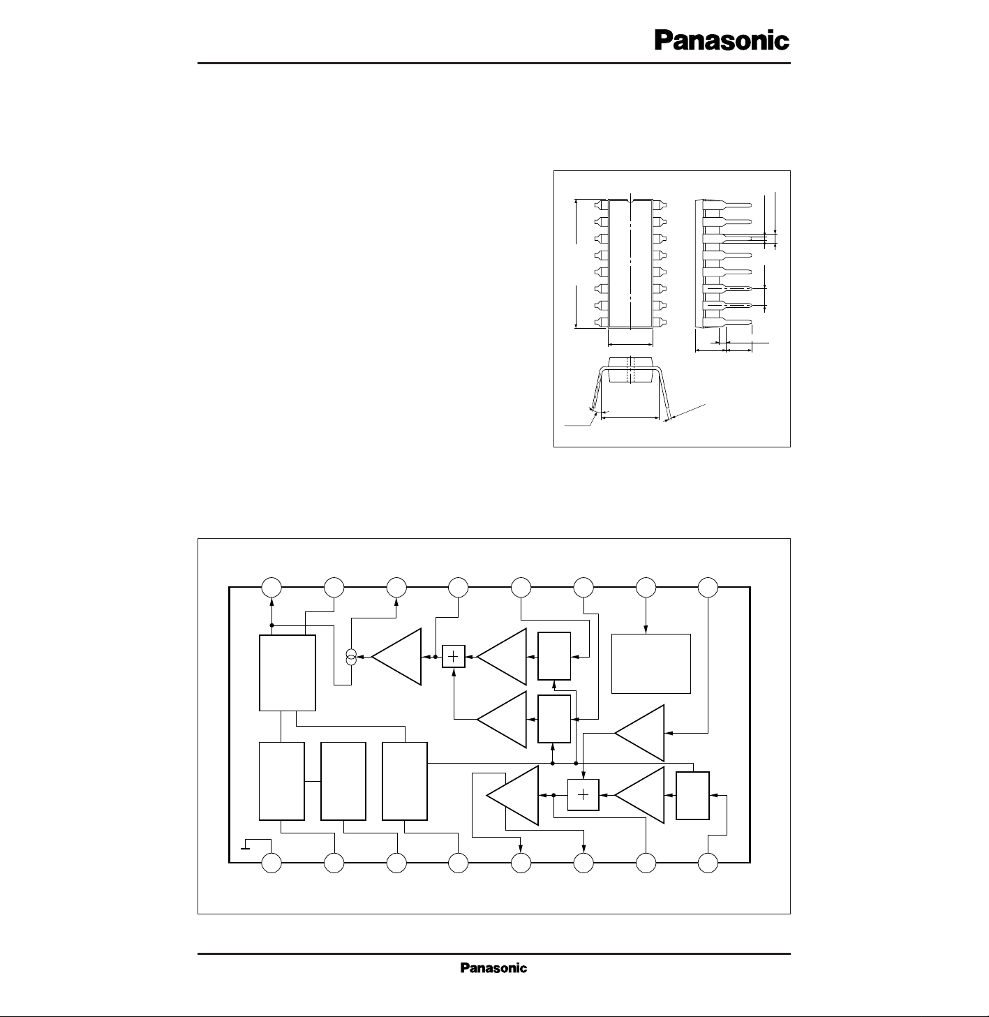
AN6150
Speech Network Circuit
1
2
3
4
5
6
7
8
16
15
14
13
12
11
10
9
19.2±0.3
1.22±0.25
3 to 15˚
Unit : mm
6.2±0.3
0.5±0.12.54
5.2±0.25 3.05±0.25
7.62±0.25
0.3
+0.1
– 0.05
1.1±0.25
16-pin DIL Plastic Package (DIP016-P-0300D)
■ Block Diagram
V
L
VLC
16 15 14 13 12 11 10 9
V-I
Control
1
GND
2V
REG
V2
1V
REG
2
ST SF
SEND
Main
Amp.
Current
Check
34
V1 AP
MIC DT DM
MIC
PreAmp.
DTMF
PreAmp.
REC
Main
Amp.
ATT
ATT
Logic
KT
PreAmp.
REC
PreAmp.
567
RO1 RO2 RF
KT
ATT
8
RI
Page 2
■ Pin Descriptions
Pin No.
Pin name
1
2
3
4
5
6
7
8
GND
2V REG.
1V REG.
ATT control
REC output
REC output
REC filter
REC input
Pin No.
Pin name
9
10
11
12
13
14
15
16
KEY In TONE input
Dial mute SW
DTMF input
MIC input
Transmission filter
SIDE tone
LIN filter
LIN
V
L
I
L
P
D
T
opr
T
stg
Line voltage
Line current
Power dissipation (Ta=60˚C)
Operating ambient temperature
Storage temperature
V
mA
mW
˚C
˚C
■ Absolute Maximum Ratings (Ta=25˚C)
14.4
135
1380
–30 to + 75
–55 to + 150
Parameter Symbol Rating Unit
■ Electrical Characteristics (IL=40mA, fin=1kHz, Ta=25˚C)
Receive System
Receiver gain
*
1
Max. receiver level
*
1
Receiver auto pad
*
1
G
V– R
–2 dBm
V
i
=–45dBm
Receiver output distortion
*
1
THD
– R
%
V
i
=–45dBm
V
O – R
dBmTHD=5%
∆AP
– R
–3 dB
V
i
=–45dBm,
DI
L
=100 to 20mA
–5.5
–7
0
1
4
–4.5
– 0.5
KEY IN TONE gain
*
1
G
V–KT
–22.5 dBm
V
i
=–40dBm,
Dial Mute SW– ON
–25 –20
5
Transmission System
Transmission gain
*
2
Max. transmission level
*
2
Transmission auto pad
*
2
G
V–T
–2 dBm
V
i
=–45dBm
Transmission output distortion
*
2
THD
–T
%
V
i
=–45dBm
V
O –T
dBmTHD=5%
∆AP
– T
–3.5 dB
V
i
=–45dBm,
DI
L
=100 to 20mA
–6.5
–6
–2.2
1
2.8
–4
–1
DTMF gain
*
2
G
V– DT
–6 dBm
V
i
=–35dBm,
Dial Mute SW– ON
–8 –4
DTMF output distortion
*
2
THD
– DT
1 %
V
i
=–35dBm,
Dial Mute SW– ON
5
DTMF auto pad
*
2
∆AP
– DT
–4 dB
V
i
=–35dBm,
DI
L
=100 to 20mA
–6 –2
5
Power Supply
DC line voltage (1)
Internal supply voltage
V
L – 1
3.6 V
I
L
=12mA
DC line voltage (2)
5.4V
L – 2
V
I
L
=127mA
V
CC
VIL=12mA
2.4
1.7
7.8
2.0
3
2.3
10.2
*
1 Connect the 1kΩ load between Pins5 and 6 for measurement.
*
2 Connect the 600Ω receiver impedance between Pins16 and 1 and measure it at the receiver side.
Parameter Symbol Condition min typ max Unit
Page 3

■ Electrical Characteristics (cont.) (IL=40mA, fin=1kHz, Ta=25˚C)
Dial Mute input
Dial mute OFF
Input current (1)
V
DM–H
V
CC
V
Dial mute ON
V
DM–L
V
I
DM–H
µAVDM=V
CC
0.8
–2.0
0.1
0.3
2.0
Input current (2) I
DM–L
µAVDM=0V –2.0 – 0.2 – 0.02
Mute
K.T. mute
*
1, 4
DTMF mute
*
2, 4
M
–KT
dB
V
i
=–15dBV,
Dial mute SW– OFF
MIC mute
*
2, 4
M
–T
dB
V
i
=–40dBV,
Dial mute SW– ON
M
–DT
dB
V
i
=–28dBV,
Dial mute SW– OFF
40
40
60
Power Supply
AC impedance (1)
*
3, 4
Z
AC–1
800 Ω
I
L
=30mA, fin=1kHz
AC impedance (2)
*
3, 4
Z
AC–2
Ω
I
L
=90mA, fin=1kHz
100µF 820Ω
400
400
670
620 800
Receiver System
K. T. output distortion
*
1, 4
THD
–KT
%
V
i
=–42dBV, IL=40mA
1
*
1 Connect the 1kΩ load between Pins5 and 6 for measurement
*
2 Connect the 600Ω receiver impedance between Pins16 and 1 measure it at the receiver side.
*
3 Connect between Pins16 and 1 for measurement.
*
4 Characteristics above are of reference valuse for design but not guaranteed values.
–+
Parameter Symbol Condition min typ max Unit
Page 4

υ
in
= –37dBV
f =1kHz
υ
in
= –47dBV
f =1kHz
Line Current I
L
(mA)
Line Voltage V
L
(V)
VL– I
L
800
700
600
500
400
300
200
100
0
0.1 0.5 1 5 10
Frequency f (kHz)
AC Impedance Z
AC
(Ω)
Z
AC
– f
8
7
6
5
4
3
2
1
0
0 40 80 120 160
Line Current I
L
(mA)
Receiver Auto Pad V
out (REC)
(dBV)
Distortion THD (%)
V
out (REC)
, THD – I
L
0
–2
–4
–6
–8
–10
–12
–14
10
8
6
4
2
0
0 40 80 120 160
Il.=50mA
Il.=20mA
Il.=80mA
Line Current I
L
(mA)
DTMF Auto Pad V
out (DTMF)
(dBV)
Distortion THD (%)
V
out (DTMF)
, THD – I
L
0
–2
–4
–6
–8
–10
–12
–14
10
8
6
4
2
0
0 40 80 120 160
Line Current I
L
(mA)
Transmission Auto Pad V
out (MIC)
(dBV)
Distortion THD (%)
V
out (MIC)
, THD – I
L
0
–2
–4
–6
–8
–10
–12
–14
10
8
6
4
2
0
0 40 80 120 160
THD
V
out
THD
V
out (MIC)
THD
V
out (DTMF)
υ
in
= –47dBV
f
=1kHz
■ Characteristics Curve
Page 5

• In case of using ceramic receiver
Diode
Bridge
T
Key in toneDTMFE C M
Ceramic
–+
–
+
AN6150
16
1
15
2
14
3
13
4
12
5
11
6
10
7
9
8
–
+
–
+
L
1
L
2
R
14
R
10
R
9
R
11
R
1
SW
1
SW
2
R
12
R
13
R
8
R
7
R
3
R
2
R
4
R
5
C
11
C
1
C
10
C
9
C
8
C
7
C
6
100µF
47µF
470µF
C
2
100µF
0.022µF
0.0022µF
0.068µF
receiver
0.068µF
C
5
C
4
C
3
0.068µF
0.068µF
0.047µF
820Ω
2.7kΩ
9.1kΩ
9.1
kΩ
620
Ω
62Ω
4.7kΩ
12kΩ
• In case of using low impedance receiver
Diode
Bridge
T
R
Key in toneDTMFE C M
Ceramic
–+
–
+
AN6150
16
1
15
2
14
3
13
4
12
5
11
6
10
7
9
8
–
+
–
+
L
1
L
2
R
14
R
10
R
9
R
11
R
1
SW
1
SW
2
R
12
R
13
R
8
R
7
R
3
R
2
R
4
R
5
R
15
C
11
C
1
C
10
C
9
C
8
C
7
C
6
100µF
47µF
470µF
C
2
100µF
0.022µF
0.0022µF
0.068µF 0.068µF
C
5
C
4
C
3
0.068µF
0.068µF
0.047µF
820Ω
2.7kΩ
9.1kΩ
9.1
kΩ
620
Ω
62Ω
4.7kΩ
12kΩ
■ Application Circuits
 Loading...