Page 1

AN-588
AD7416/AD7417/AD7418 V
DD
– V
MAINS VDD – V
0
0 0.2 0.4 0.6 0.8 1.0 1.2 1.4 1.6 1.8 2.0
0.2
0.4
0.6
0.8
1.0
1.2
1.4
1.6
1.8
2.0
MAINS
V
DD
AD7416/AD7417/AD7418
V
DD
a
APPLICATION NOTE
One Technology Way • P.O. Box 9106 • Norwood, MA 02062-9106 • Tel: 781/329-4700 • Fax: 781/326-8703 • www.analog.com
AD7416/AD7417/AD7418 Power-On Reset Circuit
By Donal McNamara
In many applications a large number of decoupling capacitors are used on the V
line to prevent any power
DD
supply noise being coupled into ICs. As a consequence
of using these noise protection capacitors, the V
DD
line
takes longer to discharge to 0 V when power is switched
off. If the time between power-off and power-on is short
enough, it is conceivable that the V
line would have
DD
only discharged to a value as high as 0.5 V. The effect
this has on the AD7416/AD7417/AD7418 is that not all of
the internal circuitry will have fully switched off. Therefore, applying power before V
has reached 0 V can cause
DD
the AD7416/AD7417/AD7418 to reset into an unknown
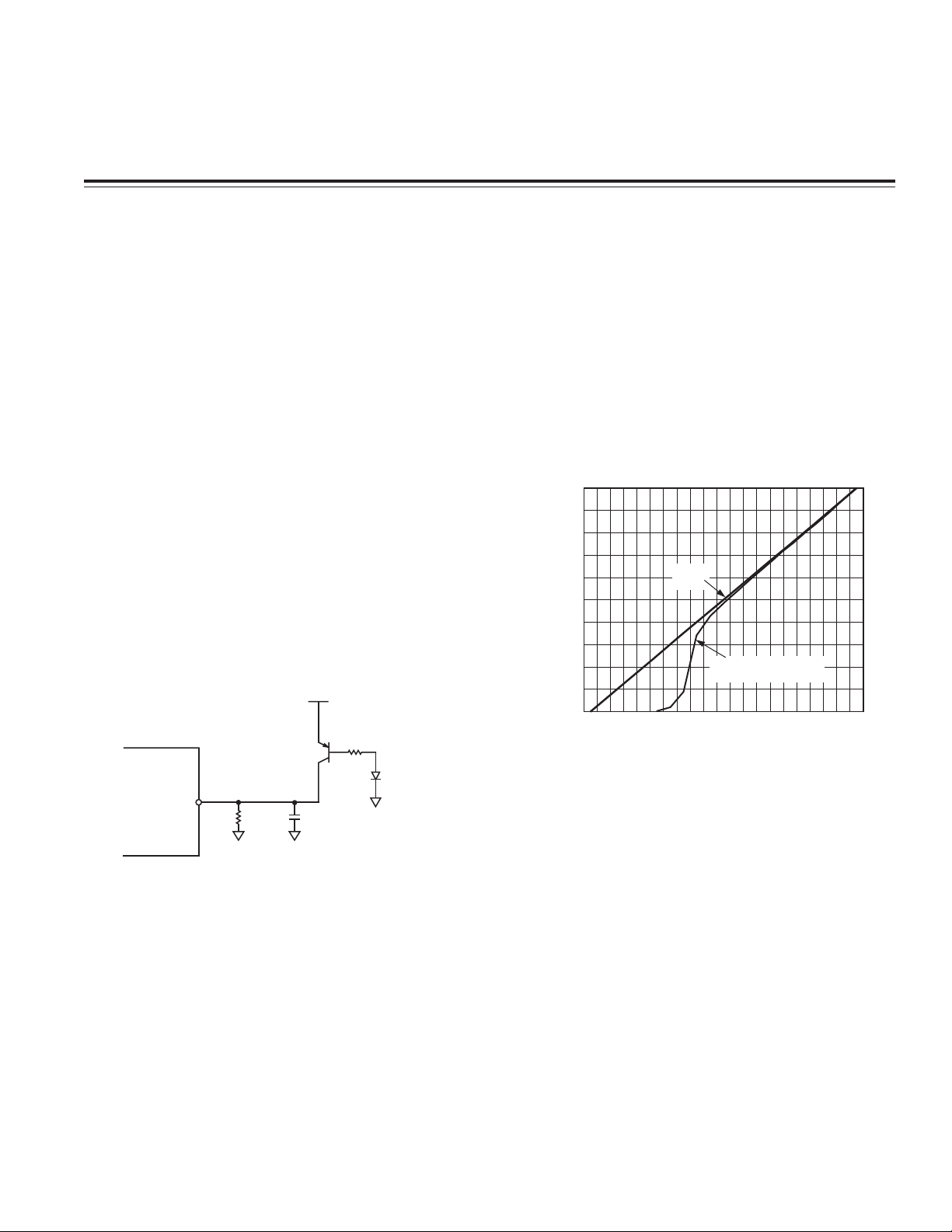
state. Figure 1 is a recommended setup in applications
where the user expects the supply voltage discharge
time to be too short for a proper power-on reset of the
AD7416/AD7417/AD7418.
The PNP transistor in Figure 1 will start switching off
when the main V
line connected to its emitter falls
DD
below approximately 1 V. At 0.5 V, the voltage on the
AD7416/AD7417/AD7418 V
pin is virtually 0 V. This cir-
DD
cuit will ensure that proper power-on reset is achieved
when power-off, power-on time is relatively short.
AD7416/
AD7417/
AD7418
V
DD
20k⍀ 10nF
Figure 1. Power-On Reset Circuit
REV. 0
MAINS V
2N5981
DD
10k⍀
1N4149
Figure 2. Voltages on Emitter and Collector of PNP
Transistor in Figure 1
© Analog Devices, Inc., 2002
Page 2

E02856–0–3/02(0)
–2–
PRINTED IN U.S.A.
 Loading...