

Page 1
ICs for TV
AN5768
TILT correction IC
■ Overview
The AN5768 is a rotation correction (TILT) IC for
CRT monitor incorporating a driving transistor. It enables
±250 mA (max.) DC current flow by connecting a coil
between the output pins which operate with a reverse
phase each other.
■ Features
• DC control input: 0 V to 5 V
• Output dynamic range: 1.2 V to 3.8 V
• Maximum output current: ±250 mA
■ Applications
• CRT monitors
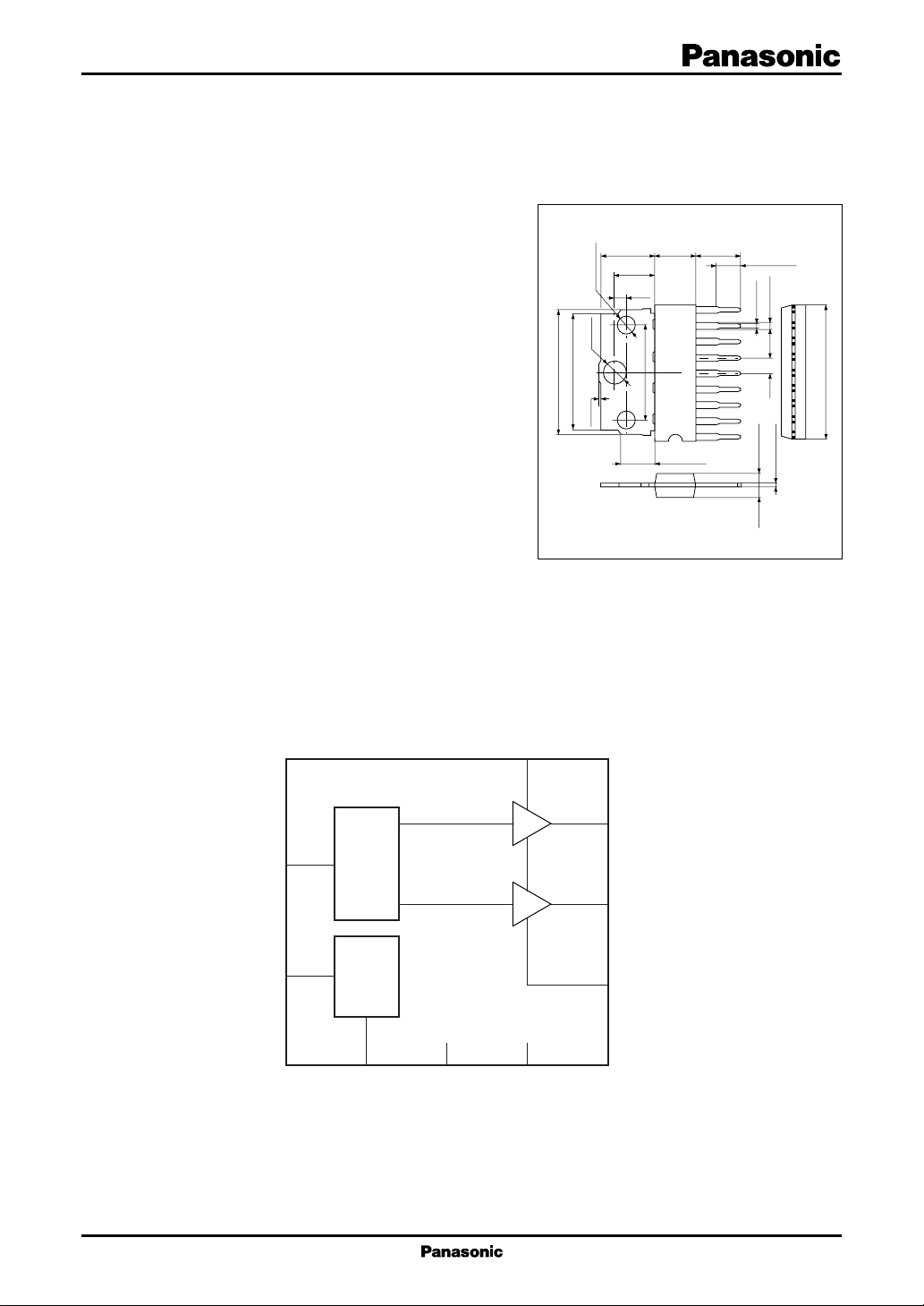
■ Block Diagram
8.4±0.25 6.3±0.3 7.1±0.25
5.8±0.25
φ2.65±0.1
1.5±0.25
φ3.3±0.1
19.9±0.1
18.3±0.25
0.1±0.05
9
8
7
6
5
4
15.0
3
2
1
5.6±0.25
HSIP009-P-0000
Unit: mm
3.75±0.25
0.5±0.1
1.2±0.25
2.54
+0.1
–0.05
0.45
1.7±0.25
±0.25
1.7
22.3±0.3
V
CC1
12 V
CC2
V
2
+
4
In
−
1
Bias
9
3
6
7
8
5
GND2
GND1
1
Page 2
AN5768 ICs for TV
■ Pin Descriptions
Pin No. Description
1 Supply voltage 12 V (V
2 Output block supply voltage 7 V (V
3N.C.
4 TILT control input
5 Output block GND (GND2)
6N.C.
7 TILT positive output
8 TILT negative output
9 GND (GND1)
■ Absolute Maximum Ratings
Parameter Symbol Rating Unit
Supply voltage V
Supply current I
2
Power dissipation
Operating ambient temperature
Storage temperature
Note)
1: Except for the operating ambient temperature and storage temperature, all ratings are for Ta = 25°C.
1. *
2: The power dissipation shown is for the IC package at Ta = 75°C.
*
2. Pay attention to an electrostatic breakdown for pin 1.
3. Observe the following sequence of the supply power start-up:
• Turn-on sequence First: Pin 2 on (7 V) power supply
• Turn-off sequence First: Pin 1 off (12 V) power supply
*
1
*
Second: Pin 1 on (12 V) power supply
Second: Pin 2 off (7 V) power supply
)
CC1
), Protective resistor is needed.
CC2
CC1
V
CC2
CC1
I
CC2
P
D
1
*
T
opr
T
stg
13.5 V
11.05
26 mA
250
1 128 mW
−25 to +75 °C
−55 to +150 °C
■ Recommended Operating Range
Parameter Symbol Range Unit
Supply voltage V
2
CC1
V
CC2
10.8 to 13.2 V
6.0 to 9.0
Page 3

ICs for TV AN5768
■ Electrical Characteristics at Ta = 25°C
Parameter Symbol Conditions Min Typ Max Unit
Circuit current 1 I
Circuit current 2 I
Circuit voltage 7 V
Circuit voltage 8 V
TILT output voltage 1 E
TILT output voltage 2 E
TILT output voltage 3 E
• Design reference data
Note) The characteristics listed below are theoretical values based on the IC design and are not guaranteed.
Parameter Symbol Conditions Min Typ Max Unit
High-level TILT output fluctuation
∆E
with supply voltage V and V
Low-level TILT output fluctuation
∆E
with supply voltage V and V
TILT output fluctuation with ∆E
temperature and Ta = +25°C → −20°C
V
CC1
CC2
7−5VCC1
8−5VCC1
T1
T2
T3
T/VCCH
T/VCCL
T/Ta
= 12 V, V
CC1
V
= 12 V, V
CC1
= 12 V, V
= 12 V, V
V7 −V8 at V4 = 2.5 V − 0.15 0 +0.15 V
V7 −V8 at V4 = 5 V +2.3 +2.5 +2.7 V
V7 −V8 at V4 = 0 V −2.7 −2.5 −2.3 V
∆E when varying V
CC2
∆E when varying V
CC2
∆E when varying Ta = 25°C → 70°C − 0.1 +0.1 V
= 7 V 16 20.5 25 mA
CC2
= 7 V 01mA
CC2
= 7 V 2.8 3.0 3.2 V
CC2
= 7 V 2.8 3.0 3.2 V
CC2
= 12 V → 13.2 − 0.1 +0.1 V
CC1
= 7 V → 9 V
= 12 V → 10.8 − 0.1 +0.1 V
CC1
= 7 V → 6 V
■ Terminal Equivalent Circuits
Pin No. Equivalent circuit Description
1 Supply voltage 12 V (V
1
V
CC1
Supply voltage pin
Apply DC 12 V.
2 Output block supply voltage 7 V (V
7 V
5 Ω
To
2
TILT output supply voltage pin
Apply DC 7 V via a protection resistor.
7
To
8To
5
3 N.C.
4 TILT control input:
V
CC1
TILT control input pin
Apply DC 0 V to 5 V.
4
(typ. = 2.5 V)
3 kΩ
GND1
): 12
CC1
CC2
DC voltage
(V)
): 7
3
Page 4

AN5768 ICs for TV
■ Terminal Equivalent Circuits (continued)
Pin No. Equivalent circuit Description
5 GND2: 0
6 N.C.
7 TILT positive output: 1.7 to 4.2
8 TILT negative output: 1.7 to 4.2
To
2
7
To To
5
2ToTo
7
5
2
To
8
Grounding pin of TILT output block
8
TILT positive output pin
Outputs in the same polarity as pin 4.
TILT negative output pin
Outputs in the polarity opposite to pin 4.
DC voltage
(V)
5
To
9 GND1: 0
9
4
GND1
12 V-system grounding pin
Page 5

ICs for TV AN5768
■ Application Circuit Example
1
2
3
4
5
6
7
8
9
V
CC1
12 V
V
CC2
CC1
V
20 µF5 Ω
7 V
6.8 kΩ
5 kΒ
• Recommended application conditions
Parameter Symbol Range Unit
TILT control input V
TILT positive output I
TILT negative output I
Peak current I
N.C.
GND2
N.C.
GND1
20 Ω
4−9
7
8
7P
I
8P
0 to 6 V
−150 to +150 mA
−150 to +150 mA
− 0.7 to +0.7 A
− 0.7 to +0.7
5
 Loading...