

Page 1

ICs for TV
AN5637
SECAM decoder IC
■ Overview
The AN5637 is a chroma signal processing circuit
for use in SECAM system. It outputs the color difference signal.
■ Features
• Built-in bell filter, deemphasis circuit
• One point adjustment
• Small number of external components
■ Applications
• SECAM system TV
16 9
18
(0.71)
Seating plane
19.2±0.3
2.54
0.5±0.1
1.22±0.25
6.2±0.3
3.55±0.051.10±0.25
5.20±0.25
7.62±0.25
3° to 15
3.05±0.25
DIP016-P-0300D
Unit : mm
°
0.30
0
.1
0
+
5
.0
0
–
1
Page 2
AN5637 ICs for TV
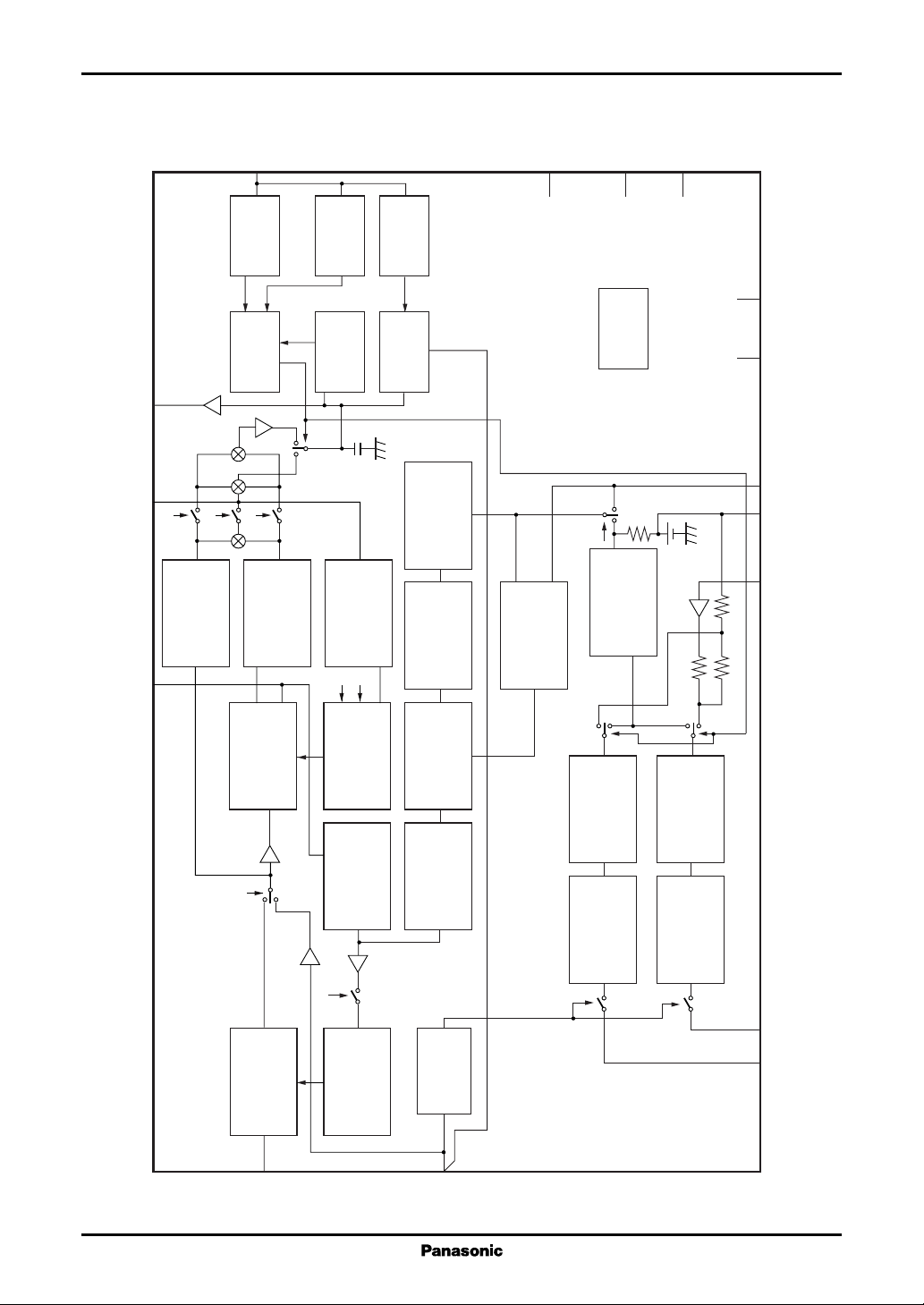
■ Block Diagram
Killer Mon.
Bell Ref.
Bell Mon.
11
7
2
Inversion
B
V
Limiter Amp.
SCP In
15
H.VBLK
generation
IH FF
B
Limiter Amp.
BGP
generation
B
generation
Reset pulse
ID discrimination
V/I conversion
B
V
VBLK
generation
V
Internal
discrimination
SECAM/Non-SECAM
V/I conversion
14
ICO
N.C.
V
N.C.
13
Band Gap
De-Emp.
12
N.C.
3
6
8
5
4
V
CC
GND
PLL Ref.
Bell Filter
Current shift
(VBLK,BGP,Signal)
B−Y Amp.
V
Limiter Amp. Phase Det. Loop Filter
Output Filter
10
9
−(B−Y) Out
−(R−Y) Out
ACC Amp.
16
C-In
B
ACC Det. Amp.
External
discrimination
SECAM/Non-SECAM
1
ref
ID/f
Output Filter R−Y Amp.
2
Page 3
ICs for TV AN5637
■ Pin Descriptions
Pin No. Description
Pin No. Description
1 Reference frequency signal/
Ident input pin
2 Bell filter output monitor pin
3 Power supply pin
4 Black level adjustment voltage input pin
5 Black level adjustment reference voltage
output pin
6 Grounding pin
7 Bell filter automatic adjustment sample
hold pin
8 PLL filter automatic adjustment sample
hold pin
9 − (R−Y) output pin
10 − (B−Y) output pin
11 Killer voltage monitor pin
12 N.C.
13 N.C.
14 N.C.
15 Sand castle pulse input pin
16 SECAM signal input pin
■ Absolute Maximum Ratings
Parameter Symbol Rating Unit
Supply voltage V
Supply current I
2
Power dissipation
Operating ambient temperature
Storage temperature
Note) *1:Ta = 25 °C except operating ambient temperature and storage temperature.
*2: Power dissipation of the package at Ta = 70 °C.
*
1
*
1
*
CC
CC
P
D
T
opr
T
stg
11.0 V
73 mA
777 mW
−20 to +70 °C
−55 to +150 °C
■ Recommended Operating Range
Parameter Symbol Range Unit
Supply voltage V
CC
■ Electrical Characteristics at VCC = 9 V, Ta = 25 °C
Parameter Symbol Conditions Min Typ Max Unit
Power supply
Supply current I
Pin voltage V
Current when VCC = 9 V 304050mA
3
Voltage when VCC = 9 V 2.9 3.2 3.5 V
5
7.2 to 9.9 V
3
Page 4

AN5637 ICs for TV
■ Electrical Characteristics at VCC = 9 V, Ta = 25 °C (continued)
Parameter Symbol Conditions Min Typ Max Unit
Input(Pin16) Typical input : (Pin16) Color bar signal, (Pin15) Sand castle pulse,
(Pin1) 4.43362 MHz sine wave 350 mV[p-p], V-BLK period
Input dynamic range V
1
Chroma signal input amplitude
*
V
Input impedance Z
Bell filter Typical input : (Pin16) 4.0 MHz to 4.6 MHz sine wave 10 mV[p-p],
Bell adjusting voltage V
Center frequency f
Band width B Band width of bell filter 250 3 10 370 kHz
ACC Typical input : (Pin16) Color bar signal (Composite) 1 V[p-p],
ACC characteristics 1 ACC1 Output change amount when −606%
ACC characteristics 2 ACC2 Output change amount when −606%
Demodulator/Output Typical input : (Pin16) Color bar signal (Composite) 1 V[p-p],
PLL adjusting voltage V
R−Y output amplitude V
B−Y output amplitude V
Detector output linearity L
R−Y/B−Y output ratio
2
Black level adjusting voltage
Black level error (R−Y)
Note) *1: Refer to "Explanations of testing method 1"
*2: Refer to "Explanations of testing method 2"
*
2
*
(R−Y)(B−Y)
V
f
Composite signal input amplitude 1.0 1.5 V
DR16
range
Chroma signal input amplitude range
ch.16
DC measurement 17 25 33 kΩ
16
300
(Pin15) Sand castle pulse,
(Pin1) 4.43362 MHz sine wave 350 mV[p-p], V-BLK period
Sample hold pin voltage at bell 2.8 3.9 5 V
ADB
filter automatic adjustement
Center frequency of bell filter 4.202 4.262 4.322 MHz
OB
(Signal period)
(Signal period)
(Pin15) Sand castle pulse,
(Pin1) 4.43362 MHz sine wave 350 mV[p-p], V-BLK period
discrimination signal changes from
150 mV[p-p] to 300 mV[p-p]
discrimination signal changes from
150 mV[p-p] to 15 mV[p-p]
(Pin15) Sand castle pulse,
(Pin1) 4.43362 MHz sine wave 350 mV[p-p], V-BLK period
Sample hold pin voltage at PLL 3.1 3.7 4.3 V
ADV
automatic adjustement
Color bar (Composite) signal input 0.85 1.00 1.15 V[p-p]
RY
(1 V[p-p])
Color bar (Composite) signal input 1.07 1.27 1.47 V[p-p]
BY
(1 V[p-p])
Color bar (Composite) signal input −606%
O
(1 V[p-p])
Amplitude ratio of VRY and V
Pin4 voltage when difference of 1.45 2.1 2.75 V
AD4
1.12 1.27 1.42 Times
BY
B−Y black level becomes 0
Value referred to input frequency 10 kHz
BER
mV[p-p]
4
Page 5

ICs for TV AN5637
■ Electrical Characteristics at VCC = 9 V, Ta = 25 °C (continued)
Parameter Symbol Conditions Min Typ Max Unit
Demodulator/Output (continued) Typical input :(Pin16) Color bar signal (Composite) 1 V[p-p],
(Pin15) Sand castle pulse,
(Pin1) 4.43362 MHz sine wave 350 mV[p-p], V-BLK period
Blanking period V
output DC voltage in V period (4.4336 MHz)
SN ratio
*
S/N Amplitude ratio when 30 dB
3
Residual high frequency amplitude V
Output impedance Z
(when SECAM) Pin9
Output impedance Z
(when non SECAM) Pin9
Output impedance Z
(when SECAM) Pin10
Output impedance Z
(when non SECAM) Pin10
Sand castle pulse Typical input : (Pin1) 4.43362 MHz sine wave 350 mV[p-p], V-BLK period
4
*
Horizontal and vertical BLK level
5
Burst gate level
*
V
V
Reference signal/interface Typical input : (Pin1) 4.43362 MHz sine wave 350 mV[p-p], V-BLK period
Reference signal amplitude V
System SW discrimination level V
IDENT Typical input : (Pin16) Color bar signal (Chroma), (Pin15) Sand castle pulse,
Color On/Off hysteresis H
Killer sensitivity K Color turn Off level when disc- −32 dB
Note) *3: Refer to "Explanations of testing method 3"
*4: Refer to "Explanations of testing method 4"
*5: Refer to "Explanations of testing method 5"
Stable sine wave is necessary 2.2 2.7 3.2 V
BLK
Deviation = 460 kHz/0 kHz
(Pin10 measurement)
Harmonic content with 100 % 10
RH
white signal input
(Pin10 measurement)
DC measurement, Pin1 = 5 V 260 460 660 Ω
OS9
DC measurement, Pin1 = 1.5 V 1 MΩ
ON9
DC measurement, Pin1 = 5 V 260 460 660 Ω
OS10
DC measurement, Pin1 = 1.5 V 1 MΩ
ON10
Measurement of slice level of H, 0.5 1 1.5 V
BL
V blanking pulse
Measurement of slice level of 3.4 3.9 4.4 V
BG
burst gate pulse
Amplitude range of sine wave 0.20 0.50 V[p-p]
ref
(4.43362 MHz) of Pin1 input
Voltage when Pin10 becomes 2.5 3.0 3.5 V
SS
open if Pin1 is 5 V to 1 V variable
(Pin1) 4.43362 MHz sine wave 350 mV[p-p], V-BLK period
Difference between color turn On 0.5 2 6 dB
C
or Off and Off to On level
rimination signal changes
150 mV[p-p] to 0 mV[p-p]
mV[p-p]
5
Page 6

AN5637 ICs for TV
■ Electrical Characteristics at VCC = 9 V, Ta = 25 °C (continued)
• Design reference data
Note) The characteristic values below are theoretical values for designing and not guaranteed.
Parameter Symbol Conditions Min Typ Max Unit
Reference signal/interface
Sink current I
Bell filter
Center frequency power supply ∆f
voltage dependency ∆V
Center frequency ambient ∆f
temperature dependency ∆T tuation when Ta = 30 °C to 80 °C
Demodulator/Output
Output signal bandwidth B
Deemphasis pole-frequency f
Pole zero point frequency ratio f
PD/fOD
R−Y output amplitude ∆V
power supply voltage dependency ∆V
R−Y output amplitude ∆VRY/ Fluctuation amount of R−Y output 0.36
ambient temperature dependency ∆T
B−Y output amplitude ∆V
power supply voltage dependency ∆V
B−Y output amplitude ∆VBY/ Fluctuation amount of B−Y output 0.55
ambient temperature dependency ∆T
Black level error (R−Y) ∆f
power supply voltage dependency ∆V
Black level error (R−Y) ∆f
ambient temperature dependency ∆T error (R−Y) when T
Black level error (B−Y) ∆f
power supply voltage dependency ∆V
Black level error (B−Y) ∆f
ambient temperature dependency ∆T error (B−Y) when T
Sink current of Pin1 when SECAM 150 175 220 µA
SS
signal input
/ Amount of center frequency fluc- 0.23 kHz/V
OB
tuation when VCC = 7.2 V to 9.9 V
CC
/ Amount of center frequency fluc- 0.25 kHz/°C
OB
Bandwidth of demodulator output 1.3 MHz
S
signal (Pin9, 10)
Automatic adjustment period 85 kHz
PD
Automatic adjustment period 3 Times
/ Fluctuation amount of R−Y output 1.5 %
RY
amplitude when VCC = 7.2 V to 9.9 V
CC
amplitude when Ta = −30 °C to +80 °C
/ Fluctuation amount of B−Y output 2.0 %
BY
amplitude when VCC = 7.2 V to 9.9 V
CC
amplitude when Ta = −30 °C to +80 °C
/ Fluctuation amount of black level 1 kHz/V
BER
error (R−Y) when VCC = 7.2 V to
CC
9.9 V
/ Fluctuation amount of black level 50 Hz/°C
BER
= −30 °C to
a
+80 °C
/ Fluctuation amount of black level 2 kHz/V
BEB
error (B−Y) when VCC = 7.2 V to
CC
9.9 V
/ Fluctuation amount of black level 90 Hz/°C
BEB
= −30 °C to
a
+80 °C
mV[p-p]
/°C
mV[p-p]
/°C
6
Page 7

ICs for TV AN5637
■ Electrical Characteristics at VCC = 9 V, Ta = 25 °C (continued)
• Explanations of testing method
1. Measurement of B−Y discrimination signal amplitude
2.
Pin15
Pin9
Pin10
∆V
R
∆V
B
Input 100 % white signal and adjust the voltage of Pin4 so that ∆V
V
.
AD4
And let the value of ∆V
based on input frequency at that time be f
R
3. Calculate by using the value of Pin10 (B−Y) output amplitude V
kHz) is input to Pin16 and the value of Pin10 output V
S/N = 20 log
10VBY/VNOISE
4. The horizontal and vertical blanking level V
5. The burst gate level V
V
= VCC × 3.8/9 (typ.)
BG
is determined by dividing the IC built-in resistor between VCC-GND.
BG
BL
is determined by the internal stabilizing power supply circuit.
when the color bar signal (Deviation = 0 Hz) is input.
NOISE
becomes 0 mV. Let the adjusted voltage be
B
, black level error (R−Y).
BER
when the color bar signal (Deviation = 460
BY
7
Page 8

AN5637 ICs for TV
■ Terminal Equivalent Circuits
Pin No. Equivalent circuit Description Voltage
1 Reference frequency signal/ AC + DC
To AN5192/95
SECAM
/Non-SECAM
discrimination
V
CC
200Ω
1
1.5kΩ 1.5kΩ
0/175µA 0/175µA
150µA
100µA 200µA
Mode
changeover
20kΩ
3.7V
Ident input Pin :
• Input and output pin for interfacing DC
with AN5192/95. 1.1 V or 4.4 V
•
The circuit becomes non-SECAM mode
if DC voltage of Pin1 becomes 3 V AC
or less. 350 mV[p-p]
• Current of 175 µA sinks into Pin1 or 0
in SECAM.
2 Bell filter output monitor pin AC + DC
V
CC
DC
4.3 V
200Ω
2
AC
200 mV[p-p]
200µA 200µA
3 Power supply pin DC : 9 V
4 Black level adjustment voltage input pin : DC
V
CC
• Monitoring −(B−Y) Out (Pin10), 1.45 V to 2.75 V
adjust Pin4 voltage so that pedestal
step difference becomes 0.
(using external volume)
5
6.8kΩ
10kΩ
15kΩ
5 Black level adjustment reference voltage DC : 3.2V
4
Black level
0.01µF
V
CC
adjustment
200µA100µA
• Pin4 voltage is generated by resistor
dividing Pin5 voltage so as not to be
affected by V
and temperature
CC
fluctuation.
output pin
3.2V
100µA 100µA 400µA
5
8
Page 9

ICs for TV AN5637
■ Terminal Equivalent Circuits (continued)
Pin No. Equivalent circuit Description Voltage
6 Grounding pin DC : 0 V
7 Bell filter automatic adjustment sample DC
V
CC
300Ω
200Ω 200Ω
300Ω
hold pin 2.5 V to 5.0 V
37.5kΩ
1mA
7
8 PLL automatic adjustment sample hold DC
V
CC
750Ω
200Ω 200Ω
8
100µA 100µA
pin 3.6 V to 3.9 V
1.5kΩ 1.5kΩ
100µA750µA
9Pin9; −(R−Y) output pin AC + DC
10 Pin10; −(B−Y) output pin
V
CC
AC
−(R−Y)
10
9
200Ω
−(B−Y)
100µA 200µA
DC : 2.9 V
9
Page 10

AN5637 ICs for TV
■ Terminal Equivalent Circuits (continued)
Pin No. Equivalent circuit Description Voltage
11 Killer voltage monitor pin DC
12 N.C.
13 N.C.
14 N.C.
15 Sand castle pulse input pin AC
V
20kΩ
CC
150µA
500Ω
100µA
1.5 V to 5 V
When SECAM more than 4 V
When non-SECAM 3 V
200Ω
Killer
circuit
11
V
CC
4.7V
2.4V
0V
200Ω
15
50µA50µA
16 SECAM signal input pin AC
V
CC
50kΩ
10pF
5kΩ
200Ω
16
50kΩ
40kΩ
2.8V
200µA 200µA100µA
40kΩ
1.0 V[p-p]
10
Page 11

ICs for TV AN5637
■ Application Circuit Example
CVBS
SECAM
Signal In
NP 2.2µF
16
SCP
75Ω
Sand Castle Pulse In
15
14
N.C.
N.C.
13
N.C.
12
11
VC
−(B−Y)Out
10
−(R−Y)Out
9
1
/ID
REF
f
Note) The following signal is inputted to Pin1 from the AN5192/95.
2
Bell
3
9V
CC
V
4
10µF
Reg.Adj.
0.01µF
0.01µF
5
Reg.1B
• System discrimination
1. Pin1 is the input and output pin for the three pieces of information
(1) Reference frequency signal input pin (AC)
(2) System discrimination signal input pin (DC voltage)
(3) SECAM/Non-SECAM discrimination output pin (DC current)
AN5637 Pin1 input
System discrimination DC voltage
Pin1 sink current Pin9, 10 output
"H" (4.6 V) 175 µA
SECAM
"L" (1.3 V) 175 µA Open
"H" (4.6 V) 0 µA DC voltage output
Non-SECAM
"L" (1.5 V) 0 µA Open
6
6.8kΩ
10kΩ15kΩ
7
1µF
8
220nF
GND
Bell Ref.
PLL Ref.
Color difference signal output
2. Reference frequency signal
The reference frequency signal input for Pin1 is used for the following 4 signals ;
(1) Bell filter automatic adjustement
(2) PLL(VCO) automatic adjustement
(3) Deemphasis automatic adjustement
(4) Ident discrimination
Be sure to input the high precision PAL carrier signal (4.43362 MHz) only in the vertical retrace period.
11
 Loading...