

Page 1
ICs for TV
AN5636K
SECAM/PAL signal conversion IC
■ Overview
The AN5636K is an IC which converts the SECAM
signal into the quasi-PAL signal. This IC can add the
SECAM signal processing function while rationalizing
the external parts in a joint use with the PAL/NTSC signal processing IC: AN5606K.
■ Features
• Rationalizing IHDL in common use with PAL IHDL
• Lowering 6H line crawling by the quasi-PAL modula-
tion
• For both auto and manual modes of signal processing
■ Applications
• TV (applicable to three systems: PAL/NTSC/SECAM)
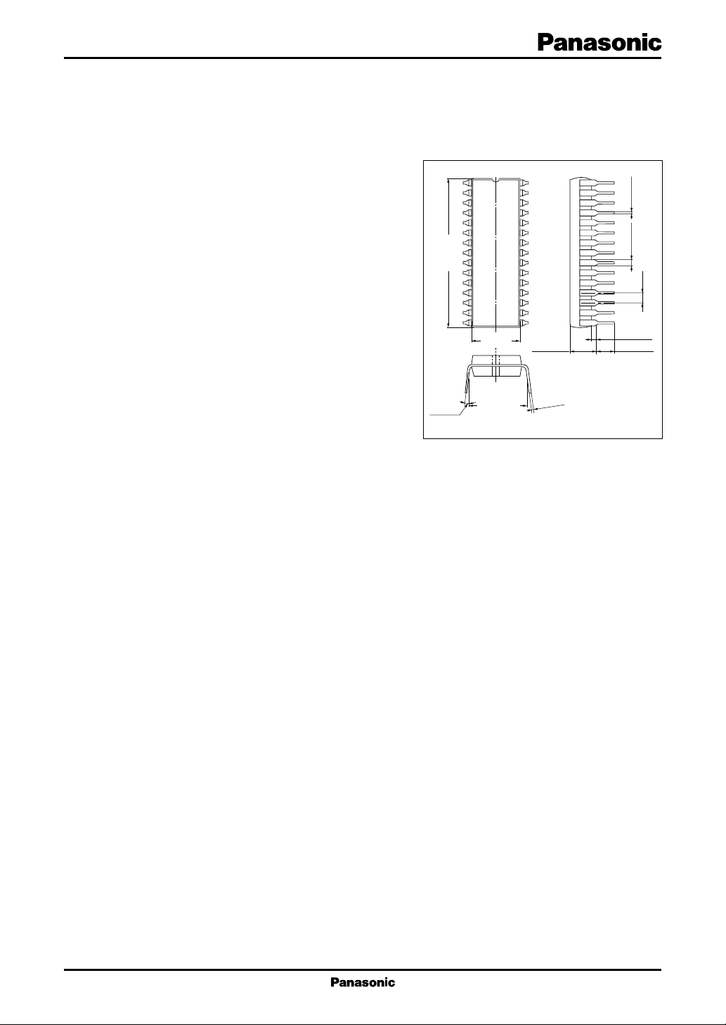
26.7±0.3
3° to 15°
1
15
8.6±0.3
10.16±0.25
SDIP030-P-0400
30
Unit: mm
0.5±0.1
0.9±0.25
1.778
16
.1
0
+
5
.0
0
−
0.35
1.0±0.25
3.3±0.254.7±0.25
1
Page 2
AN5636K ICs for T V
■ Block Diagram
(video)
CC
V
GND (video)
10
12
11
Video amp.
9
7
8
15
6
Ident.
pulse gen.
SECAM chroma
Video out
DL video
ST video
Sand castle pulse
VCC (chroma)
PAL (R − Y)
PAL (B − Y)
4.43 MHz CW
19
20
21
22
24
18
&
switch
SECAM
switch
Carrier
Phase
shifter
16
PAL matrix
PAL color killer
17
ident.
System
priority
PAL
mod.
&
reinsert
Blanking
23
4.43 MHz (chroma)
14
chroma switch
SECAM / SECAM
V. H.
blank
H.
blank
Burst
video switch
SECAM / SECAM
pulse det.
Sandcastle
13
25
Line
switch
26
27
Adder
2
28
R − Y
B − Y
clamp
clamp
pulse
Clamp
gen.
29
black
Artificial
Chroma
level
demod.
gen.
30
Flip flop
amp.
Limiter
1
2
Compo. video
GND (chroma)
5
Ident.
SECAM / SECAM
Ident.
demod.
4
3
Page 3
ICs for TV AN5636K
■ Pin Descriptions
Pin No. Description
1 GND (chroma-system)
2 SECAM chroma input
3 Limiter feedback
4 Limiter feedback
5 System discrimination holding capacitor
6 Identification pulse fall setting
7 Not SECAM video signal input
8 Sand castle pulse input
9 SECAM video signal input
10 GND (video system)
11 Video signal output
12 Not SECAM chroma signal input
13 VCC (video system)
14 PAL chroma signal output
15 Identification pulse rise setting
16 Direct signal input
Pin No. Description
17 PAL color killer voltage input
18 Delay signal input
19 VCC (chroma system)
20 R−Y signal output
21 Reference bias power supply
22 B−Y signal output
23 System identification voltage output
combined with system forcing switch
24 4.43 MHz CW input
25 Line switch output
26 R−Y clamp capacitance
27 De-emphasis circuit
28 B−Y clamp capacitance
29 Discriminator
30 Discriminator
■ Absolute Maximum Ratings
Parameter Symbol Rating Unit
Supply voltage V
Supply current I
2
Power dissipation
Operating ambient temperature
Storage temperature
Note)*1 : Except for the operating ambient temperature and storage temperature, all ratings are for Ta = 25°C.
2: Ta = 70°C, Independent IC without a heat sink
*
*
1
*
1
*
CC
CC
P
D
T
opr
T
stg
6.0 V
100 mA
600 mW
−20 to +70 °C
−55 to +150 °C
3
Page 4

AN5636K ICs for T V
■ Recommended Operating Range
Parameter Symbol Range Unit
Supply voltage V
Pin voltage V
Pin voltage V
Pin voltage V
Pin voltage V
Pin voltage V
Pin voltage V
Pin voltage V
Pin voltage V
Pin voltage V
Pin voltage V
Pin voltage V
Pin voltage V
Pin voltage V
Pin voltage V
Pin voltage V
Pin voltage V
Pin voltage V
Pin voltage V
Pin voltage V
Pin voltage V
Pin voltage V
Pin voltage V
Pin voltage V
Pin voltage V
Pin voltage V
Pin voltage V
Pin voltage V
Pin current I
Pin current I
Pin current I
Pin current I
Pin current I
Pin current I
Pin current I
CC
2-1
3-1
4-1
5-1
6-1
7-1
8-1
9-1
11-1
12-1
14-1
15-1
16-1
17-1
18-1
20-1
22-1
23-1
24-1
25-1
26-1
27-1
28-1
29-1
30-1
0 to 3 V
7-9
0 to 4.5 V
16-18
5
6
11
14
15
20
22
4.5 to 5.5 V
0 to V
0 to V
0 to V
0 to V
0 to V
0 to V
0 to V
0 to V
19-1
19-1
19-1
19-1
19-1
19-1
19-1
19-1
V
V
V
V
V
V
V
V
0 to 4.5 V
0 to V
19-1
V
0 to 4.0 V
0 to V
0 to V
0 to V
0 to V
0 to V
0 to V
0 to V
0 to V
0 to V
0 to V
19-1
19-1
19-1
19-1
19-1
19-1
19-1
19-1
19-1
19-1
V
V
V
V
V
V
V
V
V
V
0 to 4.0 V
0 to V
0 to V
0 to V
19-1
19-1
19-1
V
V
V
−1 to +1mA
0 to +2mA
−10 to 0 mA
−4 to 0 mA
0 to +2mA
−2 to 0 mA
−2 to 0 mA
4
Page 5

ICs for TV AN5636K
■ Electrical Characteristics at Ta = 25°C
Parameter Symbol Conditions Min Typ Max Unit
1. DC
Circuit current I
2. AC
Chroma block
SECAM input signal V
30 (lim)
limiting range 4.328 MHz CW of 20 mV[p-p] to
Limiter amplifier gain G
SECAM demodulation E
V30 (lim)
27 (B−Y)
output signal (B−Y) for SECAM color bar chroma of
SECAM demodulation E
27 (R−Y)
output signal (R−Y) for SECAM color bar chroma of
SECAM demodulation E
output ratio (R−Y/ B−Y)
SECAM modulation gain G
SECAM modulation V
output ratio (R−Y/ burst)
SECAM modulation V
output ratio (R−Y/ B−Y)
PAL chroma amp gain G
27 (R−Y/
B−Y)
S27-14
14 (R−Y/
burst)
14 (R−Y/
B−Y)
P12-14
Video block
Frequency characteristics
F
11SECAM
(SECAM) CW 0.3 V[p-p] input to pin 9
Frequency characteristics (PAL) F
Gain (SECAM)
Gain (PAL) G
11PAL
G
11SECAM
11PAL
Pin 13: 5.0 V, pin 13: 5.0 V 40 58 76 mA
CC1
Pin 30 output, when pin 2 input is −10+1dB
400 mV[p-p]
Pin 30 output, when pin 2 input is 18 28 38 dB
4.328 MHz CW of 2 mV[p-p]
Peak to peak voltage of DB at pin 27 159 227 29 5 mV[p-p]
200 mV[p-p] input to pin 2
Peak to peak voltage of DR at pin 27 225 321 41 7 mV[p-p]
200 mV[p-p] input to pin 2
Peak to peak voltage of DR vs. D
0.99 1.41 1.84
B
at pin 27 for SECAM color bar
chroma of 200 mV[p-p] input to pin 2
Peak to peak voltage of DR at pin 27 0.5 1.0 1.5 Times
vs. DR red at pin 14 for SECAM color
bar chroma of 200 mV[p-p] input to
pin 2
At pin 14, DR red vs. DR burst
SECAM
color bar chroma of
for
2.34 3.35 4.36
200 mV[p-p] input to pin 2
At pin 14, DR red vs. DR blue for 0.99 1.41 1.84
SECAM
color bar chroma of
200 mV[p-p] input to pin 2
Pin 14 chroma output for PAL chroma
0.7 1.0 1.3 Times
330 mV[p-p] input to pin 12
Pin 11 cutoff frequency for 1 0 MHz
Pin 11 cutoff frequency for 1 0 MHz
CW 0.3 V[p-p] input to pin 7
10 kHz CW output gain at pin 11 for 4 7 10 dB
10 kHz CW 0.3 V[p-p] input to pin 9
10 kHz CW output gain at pin 11 for 4 7 10 dB
10 kHz CW 0.3 V[p-p] input to pin 7
5
Page 6

AN5636K ICs for T V
■ Electrical Characteristics at Ta = 25°C (continued)
Parameter Symbol Conditions Min Typ Max Unit
2. AC (continued)
SECAM switch PAL matrix block
SECAM switching gain G
S16-22
(ST, B−Y) PAL chroma 660 mV[p-p] at pin 16
SECAM switching gain G
S16-20
(ST, R−Y) PAL chroma 660 mV[p-p] at pin 16
SECAM switching gain G
S18-22
(DL, B−Y) PAL chroma 660 mV[p-p] at pin 18
SECAM switching gain G
S18-20
(DL, R−Y) PAL chroma 660 mV[p-p] at pin 18
PAL matrix gain G
P16-22
(ST, +) PAL chroma 660 mV[p-p] at pin 16
PAL matrix gain G
P18-22
(DL, +) PAL chroma 660 mV[p-p] at pin 18
PAL matrix gain G
P16-20
(ST, −) PAL chroma 660 mV[p-p] at pin 16
PAL matrix gain G
P18-20
(DL, −) PAL chroma 660 mV[p-p] at pin 18
Discrimination block
SECAM killer tolerance E
Killer detection voltage
V
23SECAM
SECAM color color bar chroma of −34 dB at pin 2
Killer detection voltage V
23OFF
SECAM off color bar chroma of −50 dB at pin 2
Ident. detection voltage V
23PAL
PAL chroma burst of 150 mV[p-p] at pin 2
System switch block
System discrimination V
23SOUT
output voltage (SECAM) for PAL color bar chroma burst of
System discrimination V
23SOUT
output voltage (SECAM) for SECAM color bar chroma of
PAL chroma output at pin 22 for 0.7 1 1.3 Times
PAL chroma output at pin 20 for 0.7 1 1.3 Times
PAL chroma output at pin 22 for 0.7 1 1.3 Times
PAL chroma output at pin 20 for 0.7 1 1.3 Times
PAL chroma output at pin 22 for 0.35 0.5 0.65 Times
PAL chroma output at pin 22 for 0.35 0.5 0.65 Times
PAL chroma output at pin 20 for 0.35 0.5 0.65 Times
PAL chroma output at pin 20 for 0.35 0.5 0.65 Times
Killer on level, when SECAM color −48 −42 −36 dB
K
bar chroma 200 mV[p-p] at pin 2 is
refered as 0 dB
Pin 23 voltage for SECAM 0 0.25 0.5 V
Pin 23 voltage for SECAM 0.7 3.0 5.0 V
Pin 23 voltage for PAL color bar 0.7 3.0 5.0 V
System discrimination output at pin 23
0.7 3.0 5.0 V
150 mV[p-p] at pin 2
System discrimination output at pin 23
0 0.25 0.5 V
0 dB at pin 2
6
Page 7

ICs for TV AN5636K
■ Electrical Characteristics at Ta = 25°C (continued)
• Design reference data
Note) The characteristics listed below are theoretical values based on the IC design and are not guaranteed.
Parameter Symbol Conditions Min Typ Max Unit
1. AC
Chroma block
PAL chroma input signal voltage V
SECAM demodulation linearity LE
12(PAL)
27(R-Y)
SECAM modulation linearity LV
SECAM modulation ∆Ψ
output phase difference difference for SECAM color bar
SECAM modulation V
14(B-Y)DB
output signal (B−Y) chroma of 200 mV[p-p] input to pin 2
SECAM modulation V
14(R-Y)DR
output signal (R−Y) chroma of 200 mV[p-p] input to pin 2
SECAM modulation V
14(Burst)DR
output signal (burst) chroma of 200 mV[p-p] input to pin 2
Video block
Video input signal voltage V
9SECAM
(SECAM)
Video input signal voltage (PAL)
V
SECAM switch PAL matrix block
Direct input signal voltage V
Delay input signal voltage V
SECAM amplification degree D
S B-Y
ratio (ST/DL, B−Y) PAL chroma output ratio at pin 22
SECAM amplification degree D
S R-Y
ratio (ST/DL, R−Y) PAL chroma output ratio at pin 22
PAL amplification degree ratio DP
(ST, B−Y/R−Y) Ratio of PAL chroma output at pin 22
PAL amplification degree ratio DP
(DL, B−Y/R−Y) Ratio of PAL chroma output at pin 22
SECAM switch output phase ∆Ψ
difference (B−Y)
SECAM switch output phase ∆Ψ
difference (R−Y)
Carrier block
4.43 MHz input signal voltage V
Pin 12: PAL chroma input signal 330 660 mV[p-p]
Pin 2: 4.406 MHz ±0.28 MHz 80 90 100 %
Output linearity at pin 27
Pin 2: 4.406 MHz ±0.28 MHz 80 90 100 %
14(R-Y)
Output linearity at pin 14
At pin 14, DB vs. DR output phase 80 90 1 0 0 °
14
chroma of
200 mV[p-p] input to pin 2
blue at pin 14 for SECAM color bar
red at pin 14 for SECAM color bar
burst at pin 14 for SECAM color bar
136 227 318 mV[p-p]
192 321 450 mV[p-p]
57 96 135 mV[p-p]
Pin 9: SECAM video input 0.3 0.6 V[p-p]
Pin 7: PAL video input 0.3 0.6 V[p-p]
9PAL
Pin 16: chroma input 660 1 320 mV[p-p]
16
Pin 18: chroma input 660 1 320 mV[p-p]
18
PAL chroma input to pin 16 or pin 18 0.8 1.0 1.2
PAL chroma input to pin 16 or pin 18 0.8 1.0 1.2
Pin 16: PAL chroma input 0.8 1.0 1.2
ST
to at pin 20
Pin 18: PAL chroma input 0.8 1.0 1.2
DL
to at pin 20
Pin 22 output phase difference, when −10 0 +10 °
B-Y
PAL chroma is inputted to pin 16, pin 18
Pin 20 output phase difference, when 170 180 190 °
R-Y
PAL chroma is inputted to pin 16, pin 18
Pin 24 4.43 MHz CW input 0.3 0.5 V[p-p]
24IN
7
Page 8

AN5636K ICs for T V
■ Electrical Characteristics at Ta = 25°C (continued)
• Design reference data
Note) The characteristics listed below are theoretical values based on the IC design and are not guaranteed.
Parameter Symbol Conditions Min Typ Max Unit
1. AC (continued)
System switch block
PAL color killer input V
threshold voltage
(color)
PAL color killer input V
threshold voltage
(killer)
System-forcing switch input V
threshold voltage
(SECAM)
System-forcing switch input V
threshold voltage
(SECAM)
Pulse input block
BGP detection voltage V
H pulse detection voltage V
BLK pulse detection voltage V
Burst phase width adjusting block
Front edge threshold level V
17Color
17Color
23SIN
23SIN
THBGP
THHP
THBLKP
Input voltage at pin 17 0.5 3.0 5.0 V
Input voltage at pin 17 0 0.25 0.5 V
Input voltage at pin 23 0.5 3.0 5.0 V
Input voltage at pin 23 0 0.25 0.5 V
Pin 8: sand castle pulse 3.25 3.5 3.75 V
Pin 8: sand castle pulse input 1.8 2.2 2.6 V
Pin 8: sand castle pulse input 0.7 0.95 1.2 V
Threshold level at pin 6 1.0 1.25 1.5 V
TH6
Rear edge threshold level V
Flip-flop block
De-emphasis switch output V
(B−Y)
De-emphasis switch output V
(R−Y)
8
TH15
25B-Y
25R-Y
Threshold level at pin 15 1.0 1.25 1.5 V
Output voltage at pin 25 0 0.25 0.5 V
Output voltage at pin 25 0.5 3 . 0 5.0 V
Page 9

ICs for TV AN5636K
■ Application Circuit Example
P AL ACC chroma
Auto
System switch
VCC (chroma)
PAL (R − Y)
PAL (B − Y)
4.43 MHz CW
19
20
21
22
25
24
26
27
18
switch
SECAM
switch
Carrier
Phase
shifter
Adder
16
&
PAL matrix
Line
switch
R − Y
B − Y
28
PAL color killer
17
ident.
System
clamp
Clamp
clamp
priority
PAL
mod.
&
reinsert
Blanking
gen.
pulse
PAL
SECAM
23
Artificial
29
4.43 MHz chroma
14
chroma switch
SECAM / SECAM
V. H.
blank
H.
blank
Burst
level
black
demod.
Chroma
video switch
SECAM / SECAM
pulse det.
Sandcastle
Flip flop
gen.
Limiter
30
1
13
amp.
(video)
GND (video)
CC
V
10
12
11
Video amp.
15
Ident.
pulse gen.
Ident.
SECAM / SECAM
Ident.
demod.
2
3
9
7
8
6
5
4
SECAM chroma
Video out
DL video
ST video
Sand castle pulse
GND (chroma)
Compo. video
9
 Loading...