

Page 1
ICs for TV
AN5448
TILT correction IC
■ Overview
The AN5448 is a rotation (TILT) correction IC in
which the control circuit and the drive circuit are integrated on a single chip.
■ Features
• TILT output range: 1.7 V to 7.4 V
• Maximum output current: 200 mA
• Frequency characteristics: 200 kHz
■ Applications
• CRT monitor
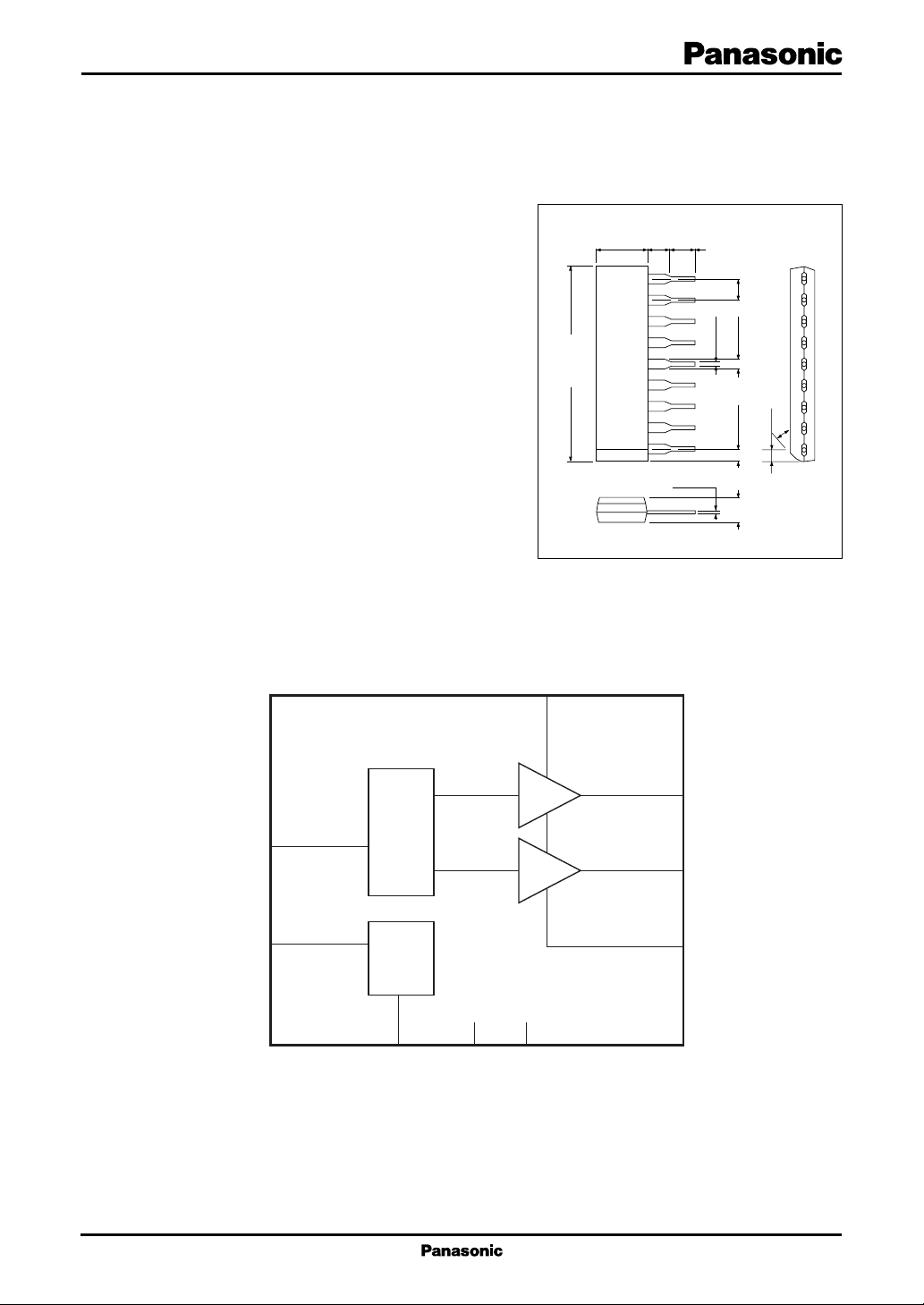
■ Block Diagram
0.5±0.1
2.54
1.5±0.25
1.5±0.25
3.0±0.3
Unit: mm
30°
1.4±0.3
CC2
V
23.3±0.3
6.0±0.3
2.4±0.25
3.3±0.25
9
8
7
6
5
4
3
2
1
+0.1
0.3
−0.05
SIP009-P-0000C
2
+
4
In
−
1
V
CC1
Bias
9
GND1
3
N.C.
6
N.C.
7
8
5
GND2
1
Page 2
AN5448 ICs for TV
■ Pin Descriptions
Pin No. Description
1 Supply voltage 12 V (V
2 Output block supply voltage 12 V (V
3N.C.
4 TILT control input
5 Output block GND (GND2)
6N.C.
7 TILT positive output
8 TILT negative output
9 GND (GND1)
■ Absolute Maximum Ratings
Parameter Symbol Rating Unit
Supply voltage V
Supply current I
2
Power dissipation
Operating ambient temperature
Storage temperature
Note) Be sure to comply with "■ Usage Notes" for the sequence of turning on power supply.
1: Except for the power dissipation, operating ambient temperature and storage temperature, all ratings are for Ta = 25°C.
*
2: The power dissipation shown is for the IC package at Ta = 75°C. Refer to "■ Technical Information" for details.
*
*
1
*
1
*
CC1
CC
CC
)
)
CC2
V
CC1
V
CC2
I
CC1
I
CC2
P
D
T
opr
T
stg
13.5 V
13.5
30 mA
200
524 mW
−20 to +75 °C
−55 to +150 °C
■ Recommended Operating Range
Parameter Symbol Range Unit
Supply voltage V
TILT control input V
TILT positive output I
TILT negative output I
Peak current I
Note) For the conditions in evaluating the peak current, refer to "■ Electrical Characteristics • Explanations of testing method".
CC1
V
CC2
4-9
7
8
7
I
8
2
10.8 to 13.2 V
7.4 to 13.2
0 to 6 V
−200 to +200 mA
−200 to +200 mA
− 0.3 to +0.3 A
− 0.3 to +0.3
Page 3

ICs for TV AN5448
■ Electrical Characteristics at Ta = 25°C
Parameter Symbol Conditions Min Typ Max Unit
Circuit current (pin 1) I
Circuit current (pin 2) I
Circuit voltage (pin 7) V
Circuit voltage (pin 8) V
Output voltage difference (1) V
Output voltage difference (2) V
Output voltage difference (3) V
7-8 (1)
7-8 (2)
7-8 (3)
• Design reference data
Note) The characteristics listed below are theoretical values based on the IC design and are not guaranteed.
Parameter Symbol Conditions Min Typ Max Unit
TILT output fluctuation
∆V
with supply voltage (high) V
TILT output fluctuation
∆V
with supply voltage (low) V
TILT output fluctuation ∆V
with temperature T
V
CC1
CC2
7-5
8-5
CC1
V
CC1
V
CC1
V
CC1
= 12 V, V
= 12 V, V
= 12 V, V
= 12 V, V
= 12 V 0.6 1.8 4.0 mA
CC2
= 12 V 01mA
CC2
= 12 V 4.1 4.5 4.9 V
CC2
= 12 V 4.1 4.5 4.9 V
CC2
V7 −V8 at V4 = 2.5 V − 0.45 0 +0.45 V
V7 −V8 at V4 = 5 V 5.3 5.7 6.1 V
V7 −V8 at V4 = 0 V −6.1 −5.7 −5.3 V
V
7-8
V
CCH
V
7-8
V
CC1
7-8/TaVIN
= 12 V → 13.2 V, ∆V
CC1
= 12 V → 13.2 V
CC2
= 12 V → 10.8 V, ∆V
CC1
= 12 V → 10.8 V
CC2
= 2.5 V, ∆V
= +25°C → +75°C and
a
at ±0.2 V
7-8
at ±0.2 V
7-8
at ±0.2 V
7-8
Ta = +25°C → −20°C
• Explanations of testing method
Conditions on evaluation of the peak current
1
2
3
4
5
6
7
8
9
V
CC
12 V
20 µF
CC1VCC2
V
24 Ω
N.C.
GND2
22 Ω/10 W
N.C.
12 V
300
A
mA
GND1
CloseOpen
6.8 kΩ
5 kB
1 s 1 s
Confirm that the IC operates normally after turning on and off SW 100 times at the interval of one second.
Carry out the above test when pin 7 is replaced with pin 8.
3
Page 4

AN5448 ICs for TV
■ Terminal Equivalent Circuits
Pin No. Equivalent circuit Description DC voltage (V)
1 Supply voltage 12 V (V
Supply voltage pin.
1
V
CC1
Apply DC 12 V.
): 12
CC1
2
12 V
2
10 Ω/2 W
7
5
8
Output-block power supply 12 V (V
CC2
Supply voltage pin for TILT output
Apply DC 12 V via a protection resistor.
):
12
3 N.C.
4 TILT control input:
Control input for TILT
V
CC1
Apply DC 0 V to 5 V. (typ. = 2.5 V)
4
3 kΩ
GND1
5 GND2: 0
2
The grounding pin for TILT output
block.
7
5
8
4
Page 5

ICs for TV AN5448
■ Terminal Equivalent Circuits (continued)
Pin No. Equivalent circuit Description DC voltage (V)
6 N.C.
7 TILT positive output: 1.7 to 7.4
2
The positive output pin for TILT
It outputs the same polarity as pin 4.
7
5
8 TILT negative output: 1.7 to 7.4
2
The negative output pin for TILT
It outputs the reverse polarity of pin 4.
8
5
9 GND1: 0
9
GND1
The grounding pin for 12 V system.
■ Usage Notes
1. The sequence of power supply turning on and off
1) Turning on sequence: First time: Pin 2 (12 V power supply)
Second time: Pin 1 (12 V power supply)
2) Turning off sequence: First time: Pin 1 (12 V power supply)
Second time: Pin 2 (12 V power supply)
If pin 2 voltage is decreased to 4.5 V or less under the established state of pin 1, an abnormal current of 20 mA
to 50 mA flows to pin 1, so that there is a possibility of breakdown of the IC. The above setting sequence should
be observed.
The normal operation of the IC has been confirmed after tuning on and off SW 100 times at the interval of 1
second with the following testing circuit. Therefore, there will be no problem even if a current under 50 mA is
allowed to flow to pin 1 for only about 1 second at turning on and turning off the set power supply. However, we
do not give you guarantee by our shipping test.
5
Page 6

AN5448 ICs for TV
■ Usage Notes (continued)
2. Testing circuit for checking abnormal current
AN5448
30 mA
CC1
V
1
V
CC
12 V
V
2
CC2
27 Ω
SW
3
V
CC
12 V
3. Principle of abnormal current generation
12 V
1
4
5
GND
6
7
8
9
GND
100 Ω
12 V→0 V
27 Ω
2
7
5
Note) The same also applies to pin 8
6
Page 7

ICs for TV AN5448
■ Usage Notes (continued)
4. The change in the output voltage by V
voltage change.
CC2
1
CC1
V
V
CC
2
CC2
V
R2
10 Ω
3
4
5
V
IN
6
7
8
9
100 Ω
If pin 2 voltage becomes a voltage of 8.3 V or less by making R2 value larger, the upper limit of TILT output voltage
is restricted and becomes as shown in figure 1.
Care must be taken at using V
at a voltage of 8.3 V or less.
CC2
(V)
7.4
4.5
TILT output voltage
1.7
0
0 2.5 5
V
IN
Figure 1
(V)
7
Page 8

AN5448 ICs for TV
■ Technical Information
• PD Ta curve of SIP009-P-0000C
T
P
D
1000
874
800
(mW)
D
600
400
Power dissipation P
200
0
0 25 150
50 75 100 125
Ambient temperature Ta (°C)
a
Independent IC
without a heat sink
R
= 143°C/W
th (j−a)
P
= 874 mW (25°C)
D
■ Application Circuit Example
1
2
3
4
5
6
V
CC
12 V
20 µF
CC1VCC2
V
10 Ω
N.C.
6.8 kΩ
5 kB
The above characteristics are reference values based on design and not guaranteed values.
*
GND2
N.C.
100 Ω/1 W
7
8
9
GND1
8
 Loading...