

Page 1
ICs for TV
AN5395FBP
Contour correction IC for HDTV
■ Overview
The AN5395FBP is a contour correction IC which
enables correction band changeover for base band HDTV,
MUSE, progressive NTSC TV.
■ Features
• Contour correction for HDTV
• Contour correction for progressive TV
■ Applications
• HDTV
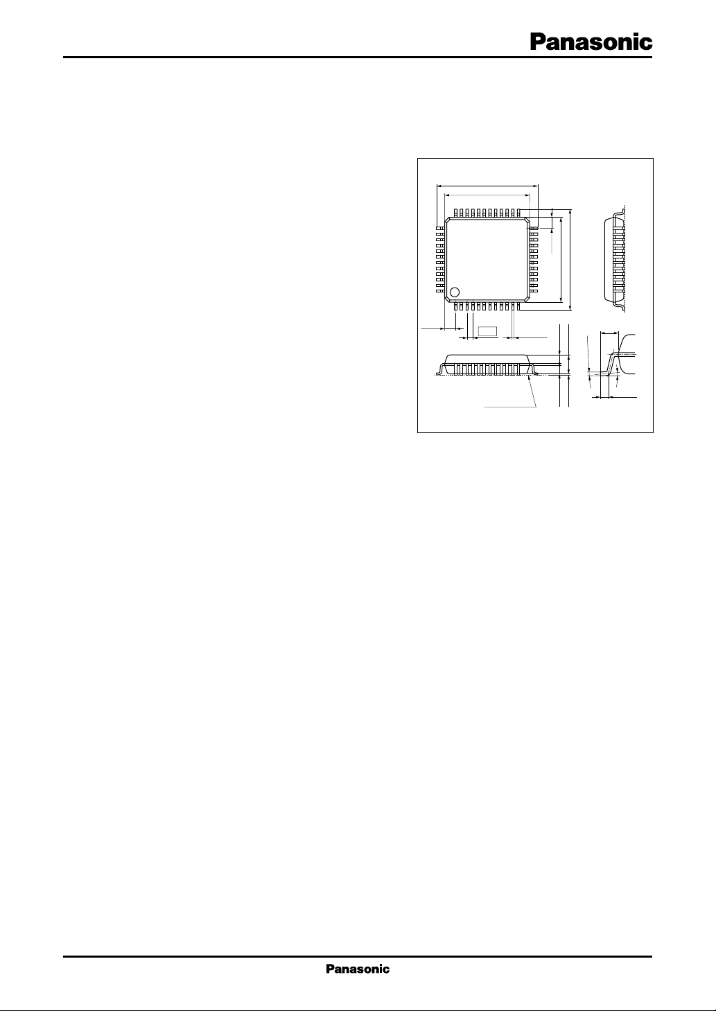
14.2±0.4
12.0±0.3
36
37
48
112
(1.60)
0.80
Seating plane
QFH048-P-1212A
25
0.3±0.1
24
13
(1.60)
12.0±0.3
1.3±0.11.3±0.1
14.2±0.4
+0.10
2.8±0.20.1±0.1
Unit: mm
(1.10)
– 0.05
0.20
0° to 10°
(0.55)
1
Page 2
AN5395FBP ICs for TV
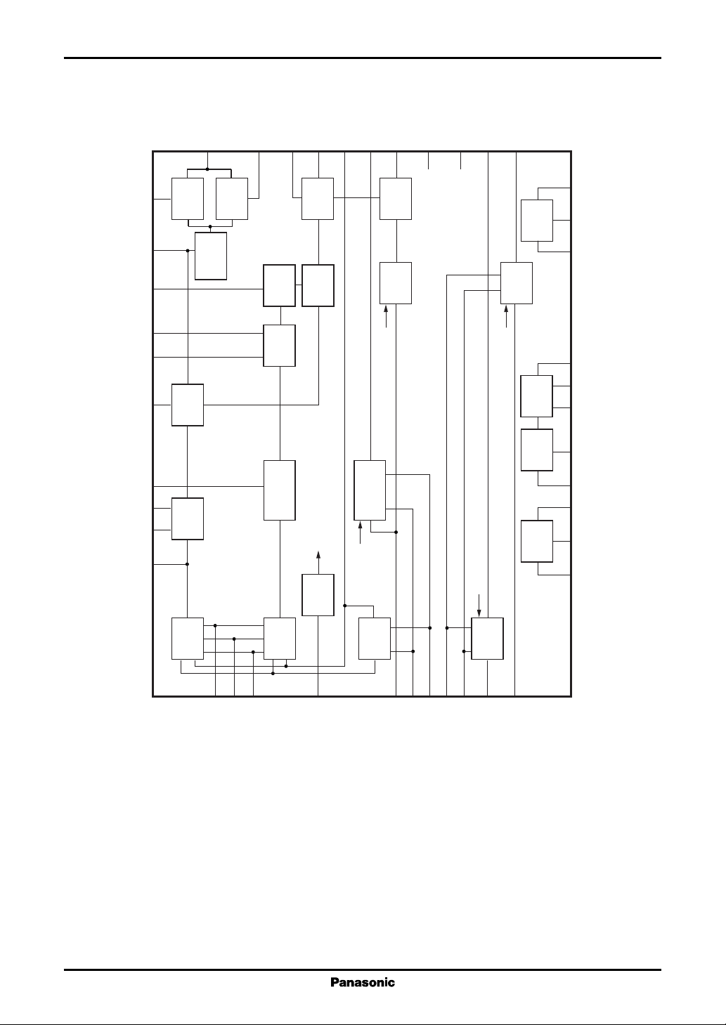
■ Block Diagram
out
42
GND
out
R
B
P
P
13
15
10
CY out
11
Gain
control
12
CY in
Delay
CC
V
Y-in
22
26
16
17
25
Y-out
27
24
19
21
Coring
Gain
control
Adder
20
28
Detector
Gain
control
Adder
Delay
Lim. out
30
29
Edge
switch
31
Gain
control
*
*
9
VM out
6
YS in
5
Fast
switch
CYS in
8
Limiter
Gain
7
4
2
control
3
VM in
32
34
33
Coring
2nd
differential
*
38
1st
differential
*
*
Clamp
Limiter Limiter
353736
Coring
Delay
43
45
394046
Y-in
Delay
48
47
1
in
in
B
R
P
P
Clamp in
2
Page 3
ICs for TV AN5395FBP
■ Pin Descriptions
Pin No. Description
1P
input
R
2 VM pre-amp. gain control
3 VM pre-amp. input
4 VM pre-amp. output
5 Child picture YS input
6Y
input
S
7 VM limiter amp. input
8 VM limiter amp. gain control
9 VM limiter amp. output
10 Child picture amp. output
11 Child picture amp. gain control
12 Child picture amp. input
13 PR output
14 N.C.
15 PB output
16 DSC large signal gain control
17
Primary differentiating input before correction
18 N.C.
19 V
CC
20 DSC detection output
21 DSC small signal gain control
22 DSC input
23 DSC bias
24 Primary differentiating output before cor-
rection
Pin No. Description
25 Sharpness mute control
26 Sharpness control
27 Y output
28 Contour block gain control
29 Contour block bias
30 Secondary differentiating input
31 Detail gain control
32
Primary differentiating output after correction
33 Detail coring control
34 Detail coring bias
35 Differentiating signal bias 1
36 Contour block and detail separation level
control
37 Differentiating signal bias 2
38 Detail limiter output
39 Y delay line changeover switch 1
40 Y delay line changeover switch 2
41 N.C.
42 GND
43 Clamp pulse input
44 N.C.
45 Y input
46 C delay line changeover switch 1
47 PB input
48 C delay line changeover switch 2
■ Absolute Maximum Ratings
Parameter Symbol Rating Unit
Supply voltage V
Supply current I
2
Power dissipation
Operating ambient temperature
Storage temperature
Note)*1: Except for the operating ambient temperature and storage temperature, all ratings are for Ta = 25°C.
2: The power dissipation shown is the value for Ta = 70°C.
*
*
1
*
1
*
CC
CC
P
D
T
opr
T
stg
10.0 V
100 mA
650 mW
−20 to +70 °C
−55 to +150 °C
3
Page 4
AN5395FBP ICs for TV
■ Recommended Operating Range
Parameter Symbol Range Unit
Supply voltage V
CC
■ Electrical Characteristics at Ta = 25°C
Parameter Symbol Conditions Min Typ Max Unit
Circuit current I
Circuit voltage V
Circuit voltage V
Circuit voltage V
Circuit voltage V
Circuit voltage V
Circuit voltage V
Circuit voltage V
Circuit voltage V
Circuit voltage V
Circuit voltage V
Circuit voltage V
Circuit voltage V
Circuit voltage V
Circuit voltage V
Circuit voltage V
Circuit voltage V
Circuit voltage V
Circuit voltage V
Circuit voltage V
Circuit voltage V
Circuit voltage V
Circuit voltage V
Circuit voltage V
Circuit voltage V
Circuit voltage V
Circuit voltage V
Circuit voltage V
Circuit voltage V
Circuit voltage V
Circuit voltage V
CC
1
2
3
4
7
9
10
11
12
13
15
16
17
21
22
24
27
29
30
31
32
33
34
35
36
37
38
39
40
45
8.1 to 9.9 V
50 70 90 mA
4.50 5.63 6.76 V
4.40 5.86 7.33 V
2.04 2.55 3.06 V
4.64 5.80 6.96 V
2.04 2.55 3.06 V
4.60 5.75 6.90 V
4.64 5.80 6.96 V
4.40 5.86 7.33 V
2.04 2.55 3.06 V
3.74 4.67 5.60 V
3.74 4.67 5.60 V
3.80 4.75 5.70 V
4.50 5.63 6.76 V
3.40 4.25 5.10 V
2.12 2.65 3.18 V
3.70 4.62 5.54 V
3.44 4.30 5.16 V
2.93 3.66 4.39 V
1.96 2.45 2.94 V
2.71 3.61 4.51 V
2.12 2.65 3.18 V
4.27 5.34 6.41 V
4.55 5.69 6.83 V
2.65 3.31 3.97 V
2.40 3.00 3.60 V
2.65 3.31 3.97 V
6.25 7.81 9.37 V
1.80 2.90 4.00 V
1.80 2.90 4.00 V
4.50 5.63 6.76 V
4
Page 5
ICs for TV AN5395FBP
■ Electrical Characteristics at Ta = 25°C (continued)
Parameter Symbol Conditions Min Typ Max Unit
Circuit voltage V
Circuit voltage V
Circuit voltage V
Circuit current I
Circuit current I
C-D.L block
PB output dynamic range V
PR output dynamic range V
Delay time changeover switch C1 V
threshold level
Delay time changeover switch C2 V
threshold level
PB signal output gain (HD) G
PB signal output gain (MUSE) G
PB signal output gain (NTSC1) G
PB signal output gain (NTSC2) G
signal output gain difference G
P
B
(MUSE/HD)
P
signal output gain difference G
B
(NTSC1/HD)
P
signal output gain difference G
B
D/A(PB)VD(PB,1)
(NTSC2/HD)
PR signal output gain (HD) G
PR signal output gain (MUSE) G
PR signal output gain (NTSC1) G
PR signal output gain (NTSC2) G
PR signal output gain difference (MUSE/HD)
PR signal output gain difference (NTSC1/HD)
PR signal output gain difference (NTSC2/HD)
PB, PR signal output gain difference (HD)
P
, PR signal output gain difference ∆G
B
G
B/A(PR)VB(PR,1) /VA(PR,1)
G
C/A(PR)VC(PR,1) /VA(PR,1)
G
D/A(PR)VD(PR,1) /VA(PR,1)
∆G
(MUSE)
, PR signal output gain difference ∆G
P
B
(NTSC1)
P
, PR signal output gain difference ∆G
B
(NTSC2)
PB signal frequency characteristics (HD)
PB signal frequency characteristics (MUSE)
PB signal frequency characteristics (NTSC1)
G
G
G
46
47
48
23
43
DR15VIN47
DR13VIN1
TH46
TH48
A(PB,1)VA(PB,1)
B(PB,1)VB(PB,1)
C(PB,1)VC(PB,1)
D(PB,1)VD(PB,1)
B/A(PB)VB(PB,1)
C/A(PB)VC(PB,1)
A(PR,1)VA(PR,1)
B(PR,1)VB(PR,1)
C(PR,1)VC(PR,1)
D(PR,1)VD(PR,1)
A(C)VA(PB,1) /VA(PR,1)
B(C)VB(PB,1) /VB(PR,1)
C(C)VC(PB,1) /VC(PR,1)
D(C)VD(PB,1) /VD(PR,1)
A(PB,F)VA(PB,20) /VA(PB,1)
B(PB,F)VB(PB,20) /VB(PB,1)
C(PB,F)VC(PB,16) /VC(PB,1)
= 5.18 V to 6.08 V 0.9 1.2 1.5 V[p-p]
= 5.18 V to 6.08 V 0.9 1.2 1.5 V[p-p]
/ 0.1 V[p-p] 1.81 2.92 3.91 dB
/ 0.1 V[p-p] 1.81 2.92 3.91 dB
/ 0.1 V[p-p] 1.81 2.92 3.91 dB
/ 0.1 V[p-p] 1.81 2.92 3.91 dB
/V
A(PB,1)
/V
A(PB,1)
/V
A(PB,1)
/ 0.1 V[p-p] 1.81 2.92 3.91 dB
/ 0.1 V[p-p] 1.81 2.92 3.91 dB
/ 0.1 V[p-p] 1.81 2.92 3.91 dB
/ 0.1 V[p-p] 1.81 2.92 3.91 dB
1.80 2.90 4.00 V
4.50 5.63 6.76 V
1.80 2.90 4.00 V
−1.50 0.00 1.50 µA
−1.50 0.00 1.50 µA
0.9 1.5 2.1 V
0.9 1.5 2.1 V
−10 1dB
−10 1dB
−10 1dB
−10 1dB
−10 1dB
−10 1dB
−10 1dB
−10 1dB
−10 1dB
−10 1dB
−6 −30dB
−6 −30dB
−6 −30dB
5
Page 6
AN5395FBP ICs for TV
■ Electrical Characteristics at Ta = 25°C (continued)
Parameter Symbol Conditions Min Typ Max Unit
C-D.L block (continued)
PB signal frequency characteristics (NTSC2)
PR signal frequency characteristics (HD)
PR signal frequency characteristics (MUSE)
PR signal frequency characteristics (NTSC1)
PR signal frequency characteristics (NTSC2)
Y-D.L block
Y output dynamic range V
Clamp pulse input threshold level V
Delay time changeover switch Y1 V
threshold level
Delay time changeover switch Y2 V
threshold level
Y signal output gain (HD) G
Y signal output gain (MUSE) G
Y signal output gain (NTSC1) G
Y signal output gain (NTSC2) G
Y signal output gain difference G
(MUSE/HD)
Y signal output gain difference G
(NTSC1/HD)
Y signal output gain difference G
(NTSC2/HD)
Y1 signal output gain (HD) G
Y1 signal output gain (MUSE) G
Y1 signal output gain(NTSC1) G
Y1 signal output gain (NTSC2) G
signal output gain difference G
Y
1
(MUSE/HD)
Y
signal output gain difference G
1
(NTSC1/HD)
Y
signal output gain difference G
1
(NTSC2/HD)
Y signal frequency characteristics (HD)
Y signal frequency characteristics G
(MUSE)
Y signal frequency characteristics G
(NTSC1)
Y signal frequency characteristics G
(NTSC2)
G
D(PB,F)VD(PB,16) /VD(PB,1)
G
A(PR,F)VA(PR,20) /VA(PR,1)
G
B(PR,F)VB(PR,20) /VB(PR,1)
G
C(PR,F)VC(PR,16) /VC(PR,1)
G
D(PR,F)VD(PR,16) /VD(PR,1)
DR27VIN45
TH43
TH39
TH40
A(Y,1)VA(Y,1)
B(Y,1)VB(Y,1)
C(Y,1)VC(Y,1)
D(Y,1)VD(Y,1)
B/A(Y)VB(Y,1) /VA(Y,1)
C/A(Y)VC(Y,1) /VA(Y,1)
D/A(Y)VD(Y,1) /VA(Y,1)
A(Y1,1)VA(Y1,1)
B(Y1,1)VB(Y1,1)
C(Y1,1)VC(Y1,1)
D(Y1,1)VD(Y1,1)
B/A(Y1)VB(Y1,1) /VA(Y1,1)
C/A(Y1)VC(Y1,1) /VA(Y1,1)
D/A(Y1)VD(Y1,1) /VA(Y1,1)
G
A(Y,F)VA(Y,30) /VA(Y,1)
B(Y,F)VB(Y,20) /VB(Y,1)
C(Y,F)VC(Y,16) /VC(Y,1)
D(Y,F)VD(Y,16) /VD(Y,1)
= 5.23 V to 6.43 V 1.2 1.6 2.0 V[p-p]
/ 0.1 V[p-p] 1.81 2.92 3.91 dB
/ 0.1 V[p-p] 1.81 2.92 3.91 dB
/ 0.1 V[p-p] 1.81 2.92 3.91 dB
/ 0.1 V[p-p] 1.81 2.92 3.91 dB
/ 0.1 V[p-p] 12 15 18 dB
/ 0.1 V[p-p] 12 15 18 dB
/ 0.1 V[p-p] 12 15 18 dB
/ 0.1 V[p-p] 12 15 18 dB
−6 −30dB
−6 −30dB
−6 −30dB
−6 −30dB
−6 −30dB
0.9 1.5 2.1 V
0.9 1.5 2.1 V
0.9 1.5 2.1 V
−10 1dB
−10 1dB
−10 1dB
−10 1dB
−10 1dB
−10 1dB
−4 −12dB
−4 −12dB
−4 −12dB
−4 −12dB
6
Page 7

ICs for TV AN5395FBP
■ Electrical Characteristics at Ta = 25°C (continued)
Parameter Symbol Conditions Min Typ Max Unit
Sharpness block
Sharpness mute switch threshold level V
Contour part max. gain V
Contour part sharpness typ. gain V
Contour part sharpness min. gain V
Contour part sharpness gain ratio
G
R.SHtyp/maxVR.SHtyp /VRmax
Detail part max. gain V
Detail part sharpness typ. gain V
Detail part sharpness min. gain V
Detail part sharpness gain ratio
Detail part sharpness mute max. gain (on)
G
S.SHtyp/maxVS.SHtyp /VSmax
V
S.SH(M.ON)
Detail part sharpness mute G
gain ratio (on/off)
(M.ON/OFF)
Contour part
Coring characteristics (on)
Coring characteristics (off)
Correction primary differentiating
V
V
V
signal gain (8 MHz)
Correction primary differentiating
V
signal gain (4 MHz)
Correction primary differentiating G
signal gain ratio
Contour gain switch (LO)
Contour gain switch gain ratio
(8M/4M)
V
G
Detail part
Typ. gain 1 V
Typ. gain 2 V
Gain ratio 1
Gain ratio 2
G
SG1typ/maxVSG1typ /VSmax
G
SG2typ/maxVSG2typ /VSmax
Detail part coring typ. gain V
Detail part coring min. gain V
Detail part coring gain ratio
G
S.COtyp/maxVS.COtyp /VSmax
Detail part limiter max. gain V
Detail part limiter typ. gain V
Detail part limiter gain ratio
G
TH25
Rmax
R.SHtyp
R.SHmin
Smax
S.SHtyp
S.SHmin
S.SHVS.SH(M.ON) /VSmax
R.CO(ON)
R.CO(OFF)
R.CO(8M)
R.CO(4M)
R.COVR.CO(8M) /VR.CO(4M)
R.SW(LO)
R.SW(L/H)VR.SW(LO) /VRmax
SG1typ
SG2typ
S.COtyp
S.COmin
S.Lmax
S.Ltyp
S.Ltyp/maxVS.Ltyp /VS.Lmax
1.10 2.65 4.20 V
1.40 1.75 2.10 V[p-p]
640 800 960
01530
mV[p-p]
mV[p-p]
−8 −6 −4dB
390 520 650
195 260 325
0510
mV[p-p]
mV[p-p]
mV[p-p]
−9 −6 −3dB
0510
mV[p-p]
−60 −50 −40 dB
210 280 350
03060
mV[p-p]
mV[p-p]
0.64 0.8 0.96 V[p-p]
1.16 1.45 1.74 V[p-p]
−7 −5 −3dB
0.88 1.1 1.32 V[p-p]
−5 −3 −1dB
210 280 350
210 280 350
mV[p-p]
mV[p-p]
−7 −5 −3dB
−7 −5 −3dB
225 315 445
0 75 150
mV[p-p]
mV[p-p]
−8 −5 −2dB
460 580 700
320 400 480
mV[p-p]
mV[p-p]
−5.5 −3.5 −1.5 dB
7
Page 8

AN5395FBP ICs for TV
■ Electrical Characteristics at Ta = 25°C (continued)
Parameter Symbol Conditions Min Typ Max Unit
DSC block
DSC detection characteristics (−35 dB)
DSC detection characteristics (−20 dB)
DSC detection characteristics (−15 dB)
DSC detection characteristics (−5 dB) V
DSC coring characteristics V
DSC limiter characteristics
Child picture amp. block
Child picture amp. max. gain G
Child picture amp. typ. gain G
Child picture amp. gain ratio
Child picture amp. G
frequency characteristics 1
Child picture amp. G
frequency characteristics 2
Child picture amp. G
frequency characteristics 3
VM pre-amp. block
VM pre-amp. max. gain G
VM pre-amp. typ. gain G
VM pre-amp. gain ratio
VM pre-amp.
frequency characteristics 1
VM pre-amp.
frequency characteristics 2
VM pre-amp. G
frequency characteristics 3
VM limiter amp. block
CYS switch threshold level V
YS switch threshold level V
Output DC step (CYS)
Output DC step (YS)
VM limiter amp. max. gain G
VM limiter amp. typ. gain G
VM limiter amp. gain ratio
VM limiter amp.
frequency characteristics 1
VM limiter amp.
frequency characteristics 2
V
DSC(−35)
V
DSC(−20)
V
DSC(−15)
DSC(−5)
D.CO(−5)
V
D.LIM(−20)
CAmax
CAtyp
G
CAtyp/maxVCAtyp
CA(20M)VCA(20M)
CA(1M)VCA(1M)
CA(F)VCA(20M) /VCA(1M)
VMPmax
VMPtyp
G
VMPtyp/maxVVMPtyp
G
VMP(20M)VVMP(20M)
G
VMP(1M)VVMP(1M)
VMP(F)VVMP(20M) /VVMP(1M)
TH5
TH6
∆V
VML(CYS)
∆V
VML(YS)
VMLmaxVVMLmax
VMLtypVVMLtyp
G
VMLtyp/maxVVMLtyp
G
VML(20M)VVML(20M)
G
VML(1M)VVML(1M)
/V
CAmax
/ 0.1 V[p-p] 9.5 11.5 13.5 dB
/ 0.1 V[p-p] 9.5 11.5 13.5 dB
/V
VMPmax
/ 0.1 V[p-p] 9.5 11.5 13.5 dB
/ 0.1 V[p-p] 9.5 11.5 13.5 dB
/ 0.1 V[p-p] 13.5 15.5 17.5 dB
/ 0.1 V[p-p] 10.5 12.5 14.5 dB
/V
VMLmax
/ 0.1 V[p-p] 12.5 14.5 16.5 dB
/ 0.1 V[p-p] 14.5 16.5 18.5 dB
2.7 3.4 4.1 V
78.79 V
6.9 8.6 9 V
0.26 0.33 0.40 V
6.9 8.6 9 V
2.7 3.4 4.1 V
10 12 14 dB
3.5 5.5 7.5 dB
−8.5 −6.5 −4.5 dB
−10 1dB
10 12 14 dB
3.5 5.5 7.5 dB
−8.5 −6.5 −4.5 dB
−10 1dB
0.45 0.75 1.05 V
0.45 0.75 1.05 V
−50 0 50 mV
−50 0 50 mV
−4.5 −2.5 − 0.5 dB
8
Page 9

ICs for TV AN5395FBP
■ Electrical Characteristics at Ta = 25°C (continued)
Parameter Symbol Conditions Min Typ Max Unit
VM limiter amp. block (continued)
VM limiter amp. G
VML(F)VVML(20M) /VVML(1M)
frequency characteristics 3
VM limiter amp.
G
VML(LIMmax)VVML(LIM.max)
/ 0.2 V[p-p] 14 16 18 dB
limiter characteristics 1
VM limiter amp.
G
VML(LIMtyp)VVML(LIM.typ)
/ 0.2 V[p-p] 6 8 10 dB
limiter characteristics 2
VM limiter amp.
G
VML(LIM)VVML(LIM.typ)
/V
VML(LIM.max)
limiter characteristics 3
YS operation characteristics G
CYS operation characteristics
VML(YS)VVML(YS)
G
VML(CYS)VVML(CYS)
/V
/V
VML(max)
VML(max)
• Design reference data
Note) The characteristics listed below are theoretical values based on the IC design and are not guaranteed.
Parameter Symbol Conditions Min Typ Max Unit
C-D.L block
PB signal delay time (HD) t
PB signal delay time (MUSE) t
PB signal delay time (NTSC1) t
PB signal delay time (NTSC2) t
signal delay time variation amount t
P
B
A(PB)
B(PB)
C(PB)
D(PB)
At DL = HD 40 50 60 ns
At DL = MUSE 52 65 78 ns
At DL = NTSC1 60 75 90 ns
At DL = NTSC2 72 90 108 ns
1(PB)tB(PB)−tA(PB)
(MUSE to HD)
P
signal delay time variation amount t
B
2(PB)tC(PB)−tA(PB)
(NTSC1 to HD)
PR signal delay time (HD) t
PR signal delay time (MUSE) t
PR signal delay time (NTSC1) t
PR signal delay time (NTSC2) t
signal delay time variation amount t
P
R
A(PR)
B(PR)
C(PR)
D(PR)
At DL = HD 40 50 60 ns
At DL = MUSE 52 65 78 ns
At DL = NTSC1 60 75 90 ns
At DL = NTSC2 72 90 108 ns
1(PR)tB(PR)−tA(PR)
(MUSE to HD)
P
signal delay time variation amount t
R
2(PR)tC(PR)−tA(PR)
(NTSC1 to HD)
PB, PR delay time difference (HD) ∆t
PB, PR delay time difference (MUSE) ∆t
PB, PR delay time difference (NTSC1) ∆t
PB, PR delay time difference (NTSC2) ∆t
A(C)tA(PB)−tA(PR)
B(C)tB(PB)−tB(PR)
C(C)tC(PB)−tC(PR)
D(C)tD(PB)−tD(PR)
−4 −20dB
−10 −8 −6dB
−36 −30 −24 dB
−36 −30 −24 dB
12 16 20 ns
20 26 32 ns
12 16 20 ns
20 26 32 ns
−60 6 ns
−60 6 ns
−60 6 ns
−60 6 ns
9
Page 10

AN5395FBP ICs for TV
G
V
2
■ Electrical Characteristics at Ta = 25°C (continued)
• Design reference data
Note) The characteristics listed below are theoretical values based on the IC design and not guaranteed.
Parameter Symbol Conditions Min Typ Max Unit
Y-D.L block
Y signal delay time (HD) t
Y signal delay time (MUSE) t
Y signal delay time (NTSC1) t
Y signal delay time (NTSC2) t
Y signal delay time variation amount t
(MUSE to HD)
Y signal delay time variation amount t
(NTSC1 to HD)
Y1 signal delay time (HD) t
Y1 signal delay time (MUSE) t
Y1 signal delay time (NTSC1) t
Y1 signal delay time (NTSC2) t
Y
signal delay time variation amount t
1
(MUSE to HD)
signal delay time variation amount t
Y
1
(NTSC1 to HD)
A(Y1)
B(Y1)
C(Y1)
D(Y1)
At DL = HD 40 50 60 ns
A(Y)
At DL = MUSE 52 65 78 ns
B(Y)
At DL = NTSC1 60 75 90 ns
C(Y)
At DL = NTSC2 72 90 108 ns
D(Y)
1(Y)tB(Y)−tA(Y)
2(Y)tC(Y)−tA(Y)
12 16 20 ns
20 26 32 ns
At DL = HD 32 40 48 ns
At DL = MUSE 40 50 60 ns
At DL = NTSC1 44 55 66 ns
At DL = NTSC2 48 60 72 ns
1(Y1)tB(Y1)−tA(Y1)
2(Y1)tC(Y1)−tA(Y1)
4812ns
10 14 18 ns
■ Terminal Equivalent Circuits
Pin No. Equivalent circuit Description
1 Pin 1: P
Pin 1
Pin 47
0.22 µF
9 V
200 Ω
200 Ω
1 kΩ 1 kΩ
4.85 V
400 µA
4.1 kΩ
2 pF
16 µA16 µA
Pin 47: PB input signal pin:
2 VM pre-amp. input pin:
44 kΩ
16 kΩ
10 kΩ10 kΩ
30 kΩ
5.6 kΩ
200 Ω
100 µA
2
0.01 µF
9 V
input signal pin:
R
•
Clamps input signal with clamp pulse of pin 43
• Drive with low impedance.
• Recommended application method: Don't apply DC voltage directly to pin.
• Control voltage: typ. 3V
• Recommended application range: 0 V to V
CC
10
Page 11

ICs for TV AN5395FBP
■ Terminal Equivalent Circuits (continued)
Pin No. Equivalent circuit Description
3 VM pre-amp. input pin:
10 µF
9 V
3
200 Ω
205 Ω 205 Ω
1 kΩ 1 kΩ 10 kΩ
10 kΩ
• Drive with low impedance.
• Recommended application method:
Don't apply DC voltage directly to pin.
2.55 V
200 µA
4 VM pre-amp. output pin:
75 µA
205
9 V
Ω
• Recommended application range:
−3.2 mA to +3.2 mA
50 Ω
50 µA
5 Pin5: Child picture YS input pin:
9 V
205 Ω
75 µA
4
6 Pin6: YS input pin:
74 kΩ
79 µA
79 µA
• Control pin for on/off of VM limiter amp.
High: Off
2 kΩ
99 µA
205 Ω
200 Ω
20 kΩ
200 Ω 200 Ω
205 Ω
200 Ω
20 kΩ
Low: On (V
• Recommended application range: 0 V to V
= 0.75 V)
TH
CC
5 6
7 VM limiter amp. input pin:
9 V
• Drive with low impedance.
200 Ω
10 µF
7
205 Ω 205 Ω
1.5 kΩ
10 kΩ
2.59 V
99 µA99 µA
10 kΩ
• Recommended application method: Don't ap-
ply DC voltage directly to pin.
11
Page 12

AN5395FBP ICs for TV
■ Terminal Equivalent Circuits (continued)
Pin No. Equivalent circuit Description
8 VM limiter amp. gain control pin:
116 kΩ
62 kΩ
101 µA
10 kΩ10 kΩ
10 kΩ
65 kΩ
200 Ω
25 kΩ
8
0.01 µF
9 V
• Control voltage: typ. 2.5 V
G
• Recommended application range: 0 V to V
9 VM limiter amp. output pin:
9 V
9
• Recommended application range:
−3.2 mA to +3.2 mA
74 µA
49 µA
205 Ω
50 Ω
205 Ω
74 µA
10 Child picture amp. output pin:
V
8
CC
75 µA
50 µA
75 µA
205 Ω
50 Ω
205 Ω
9 V
10
• Recommended application range:
−3.2 mA to +3.2 mA
11 Child picture amp. gain control pin:
44 kΩ
16 kΩ
10 kΩ10 kΩ
30 kΩ
100 µA
11
5.6 kΩ
200 Ω
0.01 µF
9 V
• Control voltage: typ. 3 V
G
V
11
• Recommended use range: 0 V to V
CC
12
Page 13

ICs for TV AN5395FBP
■ Terminal Equivalent Circuits (continued)
Pin No. Equivalent circuit Description
12 Child picture amp. input pin:
10 µF
9 V
12
200 Ω
205 Ω 205 Ω
1 kΩ 1 kΩ 10 kΩ
10 kΩ
• Drive with low impedance.
• Recommended application method: Don't apply DC voltage directly to pin.
100 µA
200 µA
205 Ω
50 Ω
411 Ω
9 V
Pin 13
Pin 15
Pin 15: P
output signal pin:
B
• Recommended application range:
−1.6 mA to +1.6 mA
2.55 V
13 Pin 13: PR output signal pin:
411 Ω
57 µA
100 µA
14 N.C. pin:
• Keep grounded
15 Refer to pin 13 Refer to pin 13
16 DSC large signal gain control pin:
15 kΩ
9.5 kΩ
3.3 kΩ
1.5 kΩ
3.75
kΩ
5 kΩ 5 kΩ
10 kΩ
42.5 kΩ
16
200 Ω
9 V
• Controls gain of large signal coring amp. on
DSC detection.
• Control voltage: typ. 3 V
G
15.25
15
kΩ
kΩ
67 µA
202 µA
47.5 kΩ
0.01 µF
• Recommended application range: 0 V to V
V
16
CC
17 Primary differentiating input pin before correction:
30.8 kΩ33.7 kΩ
20 kΩ
50 Ω
28 kΩ56.3 kΩ
339 µA
9 V
17
0.22 µF
• Y1 primary differentiating signal outputted
from pin 24 is inputted with capacitor coupling.
• Drive with low impedance.
• Recommended application method: Don't apply DC voltage directly to pin.
13
Page 14

AN5395FBP ICs for TV
G
V
21
■ Terminal Equivalent Circuits (continued)
Pin No. Equivalent circuit Description
18 N.C. pin:
• Keep grounded
19 Power supply pin:
19
20 DSC detection output pin:
1 kΩ
1 kΩ
1 kΩ
500 Ω1 kΩ
500 Ω
10 kΩ
200 Ω
200 Ω
200 Ω
60 kΩ
9 V
200 Ω
20
150 kΩ
9 V
1 kΩ
635 Ω
• Apply 9 V when use
• Controls voltage of DSC.
• Left diagram shows recommended external
circuit.
• Recommended application range:
−1.6 mA to +1.6 mA
4 700 pF
21 DSC small signal gain control pin:
9 V
• Controls gain of small signal limiter amp. on
DSC detection.
• Control voltage: typ. 3 V
0.01µF
• Recommended application range: 0 V to V
CC
15
kΩ
15 kΩ
9.5 kΩ
3.3 kΩ
1.5 kΩ
3.75
kΩ
15.25
kΩ
5 kΩ 5 kΩ
202 µA
67 µA
10 kΩ
47.5 kΩ
21
200 Ω
42.5 kΩ
22 DSC input pin:
9 V
10 kΩ10 kΩ
205 Ω205 Ω
2 kΩ 2 kΩ
2.65 V
0.9 pF
10 kΩ
211 µA
0.01 µF
22
82 µH
220 pF
1 kΩ
68 µH
27 pF
• Y signal is inputted for DSC detection.
• Left diagram shows recommended external
circuit.
• Recommended application method: Not apply
DC voltage directly to pin.
14
Page 15

ICs for TV AN5395FBP
■ Terminal Equivalent Circuits (continued)
Pin No. Equivalent circuit Description
23 DSC bias pin:
9 V
23
• No use. Keep it connected to V
• Recommended application range: 0 V to V
15 kΩ
200 Ω
CC
CC
24 Primary differentiating input pin before correction:
9 V
99 µA
205 Ω
• Output Y1 primary differentiating signal
which is made by Y signal inputted from pin
45.
• Recommended application range:
−1.6 mA to +1.6 mA
66 µA
99 µA
400 Ω
50 Ω
400 Ω
24
25 Pin 25: Sharpness mute control pin:
26 Pin 26: Sharpness gain control pin:
9 V
• Controls contour correction amount of pin 27
Y output signal by pin 26 voltage.
5.6 kΩ
200 Ω
2 V4.3 V3 V
1.125 kΩ
28 kΩ
200 Ω
11 kΩ
25
26
0.01 µF
6.6 kΩ
6.6 kΩ
V
= 3 V
26typ
Correction
amount
V
• On/off pin of contour correction signal by high/
26
low of pin 25.
44 µA165 µA
• High: Off
Low: On (VTH = 2.65 V)
• Recommended application range: 0 V to V
CC
27 Y output pin:
9 V
205 Ω
66 µA
• Outputs Y signal in which contour correction
signal has been added on Y signal inputted
50 Ω
27
from pin 45.
• Recommended application range:
−3.2 mA to +3.2 mA
66 µA
66 µA
15
Page 16

AN5395FBP ICs for TV
■ Terminal Equivalent Circuits (continued)
Pin No. Equivalent circuit Description
28 Pin 28: Contour part gain control pin:
29 Pin 29: Contour part bias pin:
205 Ω
25 kΩ15 kΩ
6.8 kΩ
29
0.0 1 µF
50 kΩ
6.8 kΩ
205 Ω
2.2 kΩ
2.2 kΩ
205 Ω
574 µA212 µA
205 Ω
1.4 kΩ
1.4 kΩ
574 µA
30 Secondary differentiating input pin:
9 V
30
0.01 µF
2.5 kΩ 2.5 kΩ
205 Ω
200 Ω
10 kΩ 10 kΩ
2.45 V
205 Ω
421 µA
25 kΩ15 kΩ
4.55 V
20 kΩ
10 kΩ
7.05 V
200 Ω
200 Ω
9V
• Contour part amp. gain can be switched in 2
steps by high/low of pin 28 voltage.
28
• High: Contour part gain high
Low: Contour part gain low (VTH = 1.5 V)
• Smoothes pin 29 signal by an external
17 kΩ
17 kΩ
capacitor.
• Recommended application range (pin 28):
0 V to V
CC
• Recommended application method (pin 29):
Don't apply DC voltage directly to pin.
• With an external circuit, differentiate the
primary differential signal that has been done
contour correction and which is outputted
from pin 32, then input it to pin 30.
• Recommended application method: Don't
apply DC voltage directly to pin.
31 Detail part gain control pin:
9 V
31
0.01 µF
1.2 kΩ
200 Ω
3 kΩ 3 kΩ
300 µA
1.2 kΩ
5.6 kΩ
5 kΩ
3.61 V
217 µA
2.2 kΩ
5 kΩ
10 kΩ
4.3 V
• Controls gain of small signal detail part amp.
by pin 31 voltage.
V
= 3 V
31typ
Detail part
gain
V
31
• Recommended application range: 0 V to V
CC
32 Primary differentiating output after correction pin:
100 µA
9 V
• Outputs a primary differentiated signal as a
signal for contour part edge switching.
50 Ω
200 Ω
32
• Recommended application range:
−1.6 mA to +1.6 mA
16
Page 17

ICs for TV AN5395FBP
■ Terminal Equivalent Circuits (continued)
Pin No. Equivalent circuit Description
33 Pin 33: Detail part coring control pin:
34 Pin 34: Detail part coring bias pin:
34
9 V
70 kΩ5.6 kΩ
4.7 kΩ
20 kΩ20 kΩ
100 µA
205 Ω
5 kΩ
3 V
204 µA75 µA
4.7 kΩ
200 Ω
0.0 1µF
100 µA
164 µA
100 µA
200 Ω
33
5 kΩ
0.01 µF
4.3 V
• Controls gain of detail part coring amp. by
pin 33 voltage.
V
= 3 V
33typ
G
• Smoothes pin 34 signal with an external
capacitor.
• Recommended application range (pin 33):
0 V to V
CC
• Recommended application method (pin 34):
Don't apply DC voltage directly to pin.
35 Differentiating signal bias 1 pin:
9 V
• Makes a necessary bias by smoothing with an
external capacitor to run a contour correction
for the primary differentiating signal inputted
from pin 17.
• Recommended application method:
Don't apply DC voltage directly to pin.
35
6.8 kΩ
205 Ω
6.8 kΩ
200 Ω200 Ω
205 Ω200 Ω
205 Ω205 Ω
5.2 kΩ
V
33
36
9 V
0.01 µF
444 µA
0 µA to 400 µA
0 µA to
400µA
352µA
Contour part and detail part separation level control pin:
• Controls separation level of contour part
60 kΩ
400 µA
(large signal) and detail part (small signal) by
pin 36 voltage
V
200 Ω
36
4.9 kΩ4.9 kΩ
5.6 kΩ
5 kΩ 6 kΩ 26.5 kΩ
= 3 V
36typ
Separation
level
30 kΩ
0.01 µF
1 kΩ
3 V
V
36
• Recommended application range: 0 V to V
CC
17
Page 18

AN5395FBP ICs for TV
■ Terminal Equivalent Circuits (continued)
Pin No. Equivalent circuit Description
37 Differentiating signal bias 2 pin:
37
9 V
6.8 kΩ
205 Ω
• Necessary bias is made by an smoothing
external capacitor in order to correct contour
of primary differentiating signal inputted
6.8 kΩ
205 Ω205 Ω
200 Ω200 Ω
from Pin17
• Recommended application method: Don't
apply DC voltage directly to pin.
5.2 kΩ
205 Ω200 Ω
0.01 µF
444 µA
0 µA to 400 µA
0 µA to
400 µA
352 µA
38 Detail part limiter output pin:
205 Ω
9 V
• Outputs detail part limiter signal
74 µA
38
50 Ω
74 µA
• Recommended application range:
−1.6 mA to +1.6 mA
39 Pin 39: Y delay line changeover switch-1 pin:
40 Pin 40: Y delay line changeover switch-2 pin:
Pin 46: C delay line changeover switch-1 pin:
9 V
Pin 48: C delay line changeover switch-2 pin:
Pins 39
• Correction amount of Y, C delay line are
40
switched by high/low of each pin voltage.
46
48
(VTH = 1.5 V)
1.5 V
41 kΩ41 kΩ
67 µA
6.1 V
40 kΩ
67 µA
1.5 V
1.8 V
6.1 V
41 kΩ41 kΩ
40 kΩ
200 Ω
1.8 V
• Pin 39, pin 46 High: Off, low: +10 ns
• Pin 40, pin 48 High: Off, low: +20 ns
• Recommended application range: 0 V to V
41 N.C. pin:
CC
42 GND pin:
18
• Keep grounded
Page 19

ICs for TV AN5395FBP
■ Terminal Equivalent Circuits (continued)
Pin No. Equivalent circuit Description
43 Clamp pulse input pin:
9 V
• Clamps inputted signal from each pin of pin
45, pin 47, pin 1 (V
• High: Clamp on
• Low: Clamp off
43
200 Ω
2.5 kΩ
• Recommended pulse width (clamp on period)
500 Ω
2 kΩ
1.51 V
NTSC: 2.5 µs
HD: 1.0 µs
• Recommended application range: 0 V to V
44 N.C. pin:
• Keep grounded
45 Y input signal pin:
9 V
1 kΩ 1 kΩ
• Clamps input signal with Pin43 clamp pulse
• Drive with low impedance
0.22 µF
45
200 Ω
200 Ω
4.1 kΩ
2 pF
• Recommended application method: Don't
apply DC voltage directly to pin.
= 1.5 V)
TH
CC
4.85 V
400 µA
16 µA16 µA
46 Refer to pin 39 Refer to pin 39
47 Refer to pin 1 Refer to pin 1
48 Refer to pin 39 Refer to pin 39
19
Page 20

AN5395FBP ICs for TV
■ Application Circuit Example (Basic Circuit)
Y-in
27 pF
68 µH
9 V
56 kΩ
0.01 µF
82 pF
3.9 kΩ
3.9 kΩ
1 kΩ
39 kΩ
1 kΩ
2.7 µH
1 kΩ
220 Ω
9 V
4 700 pF
9 V
0.0 1µF
1 kΩ
9 V
100 Ω
9 V
0.01 µF
0.01 µF
10 kΩ
635 Ω
150 kΩ
0.01 µF
0.01 µF
10 kΩ
0.01 µF
1 kΩ
Y-ou t
(9V)
CC
V
220 pF
0.01 µF
0.01 µF
9 V
0.22 µF
10 kΩ
82 µH
9 V
0.01 µF
22
21
Coring
Limiter
20
Detector
28
30
29
31
Gain
control
32
34
33
Coring
38
10 kΩ
9 V
42
19
27
24
17
25
26
16
Gain
Edge
2nd
control
switch
differential
Gain
Adder
Clamp
control
*
Adder
Delay
*
1st
differential
*
out
out
R
B
P
P
13
15
10
CY out
10 kΩ
9 V
11
Gain
Delay
*
Fast
Limiter
Gain
*
control
12
9
6
5
switch
8
7
4
2
control
3
10 µF
9 V
9 V
10 µF
0.01 µF
10 kΩ
0.01 µF
10 µF
10 kΩ
0.01 µF
CY in
VM out
in
Y
S
in
CY
S
VM in
20
9 V
Lim. out
10 kΩ
Limiter
35
0.01 µF
Coring
37
36
43
Delay
4539404648
Delay
47
1
9 V
0.01 µF
10 kΩ
0.01 µF
Clamp in
0.22 µF
9 V
Y-in
9 V
9 V
0.22 µF
0.22 µF
in
in
B
R
P
P
 Loading...