

Page 1
ICs for TV
AN5392FBQ
Luminance and color difference drive/cutoff signal processor IC
2
with I
■ Overview
converts the luminance and color difference signal into a
primary color signal. This IC supports all kinds of input
signal from hi-vision, wide, NTSC, PAL, VGA, etc. for
maximum rationalization and high performance of the
end products.
■ Features
• A wider band signal processing (Y: 30 MHz/−3 dB,
• High picture quality thanks to a large variety of built-in
• Y, C−Y signal conversion circuit built in for RGB signal
• Possible to mount in a high density thanks to SMD pack-
C bus
The AN5392FBQ is an RGB processor IC which
color difference: 15 MHz/−3 dB)
correction circuit for Y signal
for a personal computer
age
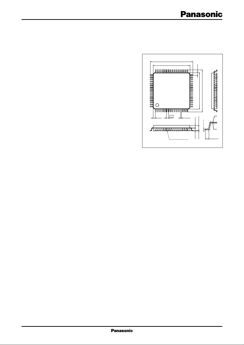
16.2±0.3
14.0±0.2
48 33
49
64
116
0.8
(1.0) 0.35
Seating plane
(1.0)
32
17
+0.10
–0.05
1.95±0.20.1±0.1
0.9±0.1 0.9±0.1
QFS064-P-1414
Unit: mm
16.2±0.3
14.0±0.2
+0.10
–0.05
.15
0
0.55±0.2
■ Applications
• Hi-vision TV, wide TV, projection TV, plasma display
panel (PDP)
1
Page 2
AN5392FBQ ICs for TV
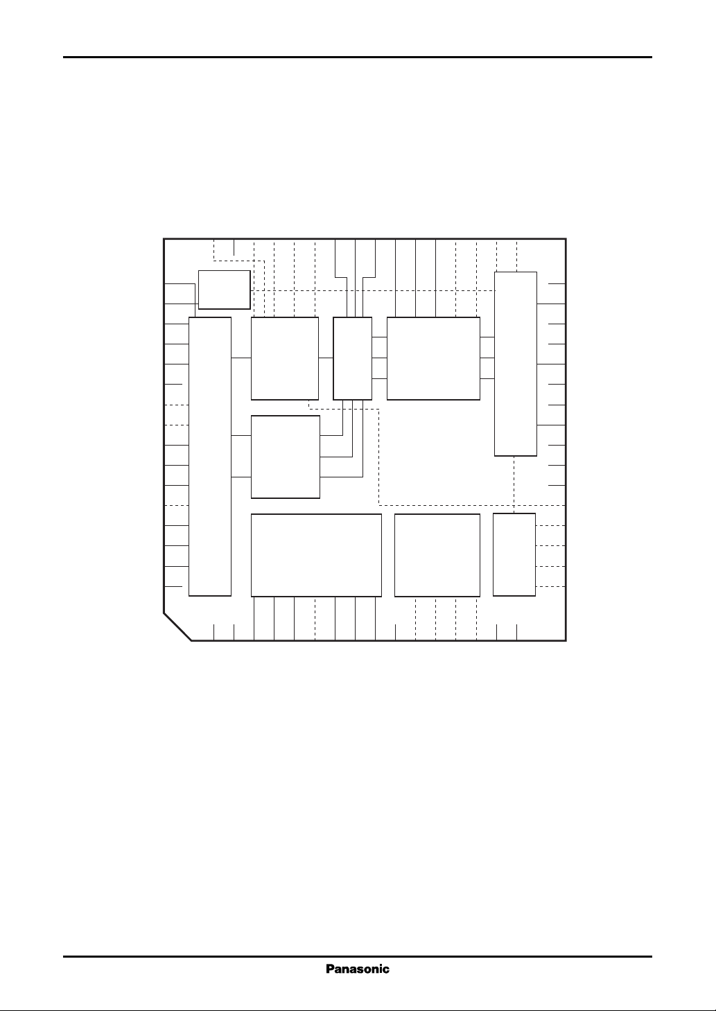
■ Block Diagram
CC
in
in
M
DC regenaration rate
Analog V
Blooming level in
Black peak det.
4847464544
White peak det.
APL det.
R-CLP
G-CLP
41
43
42
B-CLP
40
OSD-R in
39
38
S
OSD-G in
Y
OSD-B in
Y
3736353433
R, G, B limiter in
Spot killer in
VM out
ABL/ACL in
R−Y (S) in
Y (S) in
B−Y (S) in
Y, U, V V
CC
M/S in
CLP (M1) in
R−Y (M1) in
Y (M1) in
B−Y (M1) in
CLP (M2) in
R−Y (M2) in
Y (M2) in
B−Y (M2) in
Y, U, V GND
49
50
51
52
53
54
55
56
57
58
59
60
61
62
63
64
ABL/ACL
block
Y Y G
Video
block
R−Y
Input
block
Chrominance
B−Y
block
R, G, B → Y, U, V
3
1
2
4
5
L GND
2
I
Y-out
B−Y out
R,G,B GND
Matrix
block
R−Y
G−Y
B−Y
block
6
7
8
R-in
R−Y out
CLP (R, G, B) in
G-in
R
B
9
B-in
10
CC
R, G, B V
SW
block
I2C DAC
block
11
in
P
V
R
G
Output
block
B
BLK
block
1213141516
CC
SCL
SDA
L V
2
I
Slave address SW
32
31
30
29
28
27
26
25
24
23
22
21
20
19
18
17
Pulse GND
G-V
CC
G-out
G-GND
B-V
CC
B-out
B-GND
R-V
CC
R-out
R-GND
Analog GND
Pulse V
CC
DI in
CRT mute
Neck mute
R,G,B mute
BLK in
2
Page 3
ICs for TV AN5392FBQ
■ Pin Descriptions
Pin No. Description
1I
2
L GND
2 R, G, B GND
3B−Y output
4 Y-output
5R−Y output
6 CLP (R, G, B) input
7 R-input
8 G-input
9 B-input
10 R, G, B V
CC
11 VP input
12 Slave address SW
13 SDA
14 SCL
15 I2L V
CC
16 Pulse GND
17 BLK input
18 R, G, B mute input
19 Neck mute input
20 CRT mute input
21 DI input
22 Pulse V
CC
23 Analog GND
24 R-GND
25 R-output
26 R-V
CC
27 B-GND
28 B-output
29 B-V
CC
30 G-GND
31 G-output
32 G-V
CC
Pin No. Description
33 Spot killer input
34 R, G, B limiter input
35 YM input
36 YS input
37 OSD-B input
38 OSD-G input
39 OSD-R input
40 B-CLP filter
41 G-CLP filter
42 R-CLP filter
43 APL detection filter
44 White peak detection filter
45 Black peak detection filter
46 Blooming level input
47 Analog V
CC
48 DC regenaration rate
49 VM output
50 ABL/ACL input
51 R−Y (S) input (Pr (S) input)
52 Y (S) input
53 B−Y (S) input (Pb (S) input)
54 Y, U, V V
CC
55 M/S input
56 CLP (M1) input
57 R−Y (M1) input (Pr (M1) input)
58 Y (M1) input
59 B−Y (M1) input (Pb (M1) input)
60 CLP (M2) input
61 R−Y (M2) input (Pr (M2) input)
62 Y (M2) input
63 B−Y (M2) input (Pb (M2) input)
64 Y, U, V GND
3
Page 4
AN5392FBQ ICs for TV
■ Absolute Maximum Ratings
■ Absolute Maximum Ratings
Parameter Symbol Rating Unit
Supply voltage V
Supply current I
2
Power dissipation
*
Operating ambient temperature
1
Storage temperature
Note)*1: Except for the operating ambient temperature and storage temperature, all ratings are for Ta = 25°C.
2: The power dissipation PD shown is for the independent IC without a heat sink in the free air at Ta = 70°C.
*
*
CC
CC
1
*
■ Recommended Operating Range
Parameter Symbol Range Unit
V
CC1
V
CC2
I
CC1
I
CC2
P
D
T
opr
T
stg
10.0 V
5.6
70.0 mA
34.0
685 mW
−20 to + 70 °C
−55 to + 150 °C
Supply voltage V
■ Electrical Characteristics at V
CC1
V
CC2
= 9 V, V
CC1
= 5 V, Ta = 25°C
CC2
8.1 to 9.9 V
4.5 to 5.5
Parameter Symbol Conditions Min Typ Max Unit
DC characteristics
Circuit current 1
*
I
CC1
V
CC1
= 9 V, V
= 5 V 395163mA
CC2
1
No signal input
1
Circuit current 2
*
I
CC2
V
CC1
= 9 V, V
= 5 V 202530mA
CC2
No signal input
Y-system
Video voltage gain AY
Input: Sine wave 0.2 V[p-p] 4.7 5.6 6.7 Times
G
f = 1 MHz, contrast: max.
Video voltage gain ∆AY Ratio between R,G and B −2.5 0 +2.5 dB
variation amount Drive: typ.
Frequency characteristics f
Input: Sine wave 0.2 V[p-p] −6 −3 +1dB
Y
f = 30 MHz, contrast: max.
Typical output pedestal DC
Brightness variable range V
Contrast ratio A
APL detection voltage V
Brightness: typ. 2.6 3.0 3.4 V
P
Brightness: min. → max. 1.8 2.2 2.6 V
BR
Contrast: min. → max. 25 30 dB
CON
Input: Total white 0.7 V[0-p] 0. 7 1.0 1.3 V
APL
APL detection pin 43 voltage
APL detection ratio ∆
Input: Total white 0.7 V[0-p] → 0.35 V[0-p]
APL
0.46 0.54 0.66 Times
APL detection pin 43 voltage ratio
Note)*1: I
is a total amount of the current flowing through pin 10, pin 26, pin 29, pin 32, pin 47 and pin 54.
CC1
I
is a total amount of the current flowing through pin 15 and pin 33.
CC2
4
Page 5
ICs for TV AN5392FBQ
■ Electrical Characteristics at V
= 9 V, V
CC1
= 5 V, Ta = 25°C (continued)
CC2
Parameter Symbol Conditions Min Typ Max Unit
Y-system (continued)
DC regeneration ratio 1 DC
Input signal: APL 10% → 90%, 96 102 107 %
1
APL det. pin 0 V
DC regeneration ratio 2 DC
Input signal: APL 10% → 90%, 65 75 85 %
2
DC regeneration SW/on, polarity: −
DC regeneration ratio 3 DC
Input signal: APL 10% → 90%, 115 125 1 3 5 %
3
DC regeneration SW: On, polarity: +
Output blooming level V
Blooming DC = 3.8 V, 5.7 6.7 7.7 V
BL
pin 43: 0 V, brightness: max.
Output blooming level ∆V
Blooming DC = 3.8 V → 4.2 V, −1.18 − 0.93 − 0.68 V
BL
variation amount pin 43: 0 V, brightness: max.
2
White gradation correction 1
*
Yγ
Gain: max., level: typ. → max. 9.0 14 18.0 %
1
White gradation SW: On
White gradation correction 2
Yγ
Gain: max., level: typ. → min. −24 −18 −12 %
2
2
*
White gradation SW: On
Black extension Y
3
characteristics 1
*
Black extension Y
3
characteristics 2
*
Black extension Y
3
characteristics 3
*
Black extension Y
4
characteristics 4
*
Black extension Y
4
characteristics 5
*
Black extension Y
4
characteristics 6
White character correction 1
*
2
*
V
Output amplitude: 0 V[p-p] − 0.1 0 +0.1 V
BL1
Level: typ., gain: min. → max.
Output amplitude: 1.0 V[0-p] − 0.49 − 0.37 − 0.25 V
BL2
Level: typ., gain: min. → max.
Output amplitude: 2.2 V[0-p] − 0.1 0 +0.1 V
BL3
Level: typ., gain: min. → max.
Black detection: Open → 3 V −1.10 − 0.82 − 0.55 V
BL4
Level: typ., gain: typ.
Black detection: Open → 3 V −2.00 −1.55 −1.00 V
BL5
Level: typ., gain: max.
Black detection: Open → 3 V − 0.48 − 0.30 − 0.12 V
BL6
Level: min. → max., gain: typ.
Blooming DC adjustment 10.0 25.0 40.0 %
W1
Level: max., gain: min. → typ.
2
White character correction 2
*
V
Blooming DC adjustment −9.3 0 9.3 %
W2
Level: min., gain: min. → max.
White character correction off
W
OFFPR
, PB input: +0.2 V[p-p] − 0.2 0 +0.2 V
2
*
Level: max., gain: min. → max.
5
ABL off
*
V
ABL1
ABL/ACL pin: 7.5 V − 0.1 0 +0.1 V
Level: min., gain: min. → max.
5
ABL start 1
*
V
ABL2
ABL/ACL pin: 3 V 0.28 0.39 0.50 V
Level: min. → max., gain: max.
Note)*2: Control a blooming DC voltage (pin 46)
3: Black gradation SW: On
*
4: Black gradation SW: On, brightness: max.
*
5: ABL SW: On, brightness: max.
*
5
Page 6
AN5392FBQ ICs for TV
■ Electrical Characteristics at V
= 9 V, V
CC1
= 5 V, Ta = 25°C (continued)
CC2
Parameter Symbol Conditions Min Typ Max Unit
Y-system (continued)
ABL start 2
*
V
ABL3
ABL/ACL pin: 3 V − 0.84 − 0.64 − 0.44 V
5
Level: min., gain: min. → max.
5
ABL gain 1
*
A
ABL/ACL pin: 5 V → 3 V − 0.48 − 0.37 − 0.26 V
ABL
Level: typ., gain: max.
6
ACL off
*
A
ACL1
ABL/ACL pin: 7.5 V −50+5%
Level: min., gain: min. → max.
ACL start 1
*
A
ACL2
ABL/ACL pin: 3 V 10 20 30 %
6
Level: min. → max., gain: typ.
6
ACL start 2
*
A
ACL3
ABL/ACL pin: 3 V −45 −35 −25 %
Level: min., gain: min. → typ.
6
ACL gain 1
*
A
ACL4
ABL/ACL pin: 5 V → 3 V −34 −22 −10 %
Level: typ., gain: typ.
Color difference-system
Color difference voltage gain
G
Input: Sine wave 0.2 V[p-p] 9.5 11.4 13.7 Times
R
7
*
f = 1 MHz, R−Y in → R-out
Color difference frequency fc Input: Sine wave 0.2 V[p-p] − 6 − 3 + 2dB
7
characteristics
B−Y axis gain adjusting range G
NTSC 1
B−Y axis gain adjusting range G
NTSC 2
B−Y axis gain adjusting range G
*
HD 1
B−Y axis gain adjusting range G
*
HD 2
Tint variable range T
*
7
*
7
*
7
7
f = 10 MHz
B−Y gain: min., brightness: max. 0.28 0.45 0.61 Times
B-Y1
Tint SW: NTSC
B−Y gain: max., brightness: max. 1.00 1.25 1.60 Times
B-Y2
Tint SW: NTSC
B−Y gain: min., brightness: max. 0.50 0.78 1.18 Times
B-Y3
Tint SW: HD
B−Y gain: max., brightness: max. 1.18 2.00 2.80 Times
B-Y4
Tint SW: HD
Tint: min. → max. ± 33 ± 48 ± 68 °
C
B−Y gain, drive RB: Adjustment
7
Color control
*
C
Color: typ. → max. 3 6 9 dB
CON
Contrast: typ.
7
Color residue
*
C
Color: min., B−Y gain: max. − 50 0 +50 mV[p-p]
MIN
Contrast: max.
7
R−Y angle adjusting range
Note)*5: ABL SW: On, brightness: max.
6: ACL SW: On
*
7: Adjust tint, drive R, B.
*
*
θ
R−Y axis: min. → max. 10 17 24 °
R
6
Page 7
ICs for TV AN5392FBQ
■ Electrical Characteristics at V
= 9 V, V
CC1
= 5 V, Ta = 25°C (continued)
CC2
Parameter Symbol Conditions Min Typ Max Unit
Color difference-system (continued)
Matrix ratio M1 Tint SW: HD 0.23 0.30 0.35 Times
7
(G−Y/R−Y) HD
*
G−Y matrix: HD
Matrix ratio M2 Tint SW: NTSC 0.38 0.51 0.58 Times
7
(G−Y/R−Y) NTSC 1
*
G−Y matrix: NTSC 1
Matrix ratio M3 Tint SW: NTSC 0.26 0.34 0.40 Times
7
(G−Y/R−Y) NTSC 2
*
G−Y matrix: NTSC 2
Matrix ratio M4 Tint SW: NTSC 0.26 0.34 0.40 Times
7
(G−Y/R−Y) NTSC 3
*
G−Y matrix: NTSC 3
Matrix ratio M5 Tint SW: HD 0.07 0.10 0.13 Times
7
(G−Y/B−Y) HD
*
G−Y matrix: HD
Matrix ratio M6 Tint SW: NTSC 0.15 0.19 0.23 Times
7
(G−Y/B−Y) NTSC 1
*
G−Y matrix: NTSC 1
Matrix ratio M7 Tint SW: NTSC 0.22 0.28 0.34 Times
7
(G−Y/B−Y) NTSC 2
*
G−Y matrix: NTSC 2
Matrix ratio M8 Tint SW: NTSC 0.13 0.17 0.21 Times
7
(G−Y/B−Y) NTSC 3
*
G−Y matrix: NTSC 3
OSD
8
input threshold voltage
Y
S
*
Y
Pin 36 > 2.1 V: OSD 0.9 1.5 2.1 V
STH
Pin 36 < 0.9 V: Main & sub
8
M/S input threshold voltage
*
M/S
Pin 55 > 2.1 V: Sub 0.9 1.5 2.1 V
TH
Pin 55 < 0.9 V: Main (M1, M2)
8
input threshold voltage
Y
M
*
Y
Pin 35 > 2.1 V: Half tone 0.9 1.5 2.1 V
MTH
Pin 35 < 0.9 V: Main & sub
CLP input threshold voltage CLP
Pin 56, 60 (main, sub, OSD) 0.9 15 2.1 V
TH
Pin 6 (RGB)
Pulse width can be clamped W
Pin 56, 60 (main, sub, OSD) 0.8 µs
M
Pin 6 (RGB)
OSD gain G
Input: Sine wave 0.2 V[p-p] 5.0 6.0 7.2 Times
OSD
f = 1 MHz, YS pin: 5 V
OSD frequency characteristics f
OSD
Input: Sine wave 0.2 V[p-p] −7 −3 +1dB
f = 30 MHz, YS pin: 5 V
OSD contrast ratio 1 OSD
Contrast: max. → typ. −3 −1 +1dB
C1
YS pin: 5 V
OSD contrast ratio 2 OSD
Contrast: typ. → min. −16 −11 −7dB
C2
YS pin: 5 V
Note)*7: Adjust tint, drive R, B
8: SW priority: YS > M/S > M1/M2 (I2C), YS: YM is valid at low.
*
7
Page 8

AN5392FBQ ICs for TV
■ Electrical Characteristics at V
= 9 V, V
CC1
= 5 V, Ta = 25°C (continued)
CC2
Parameter Symbol Conditions Min Typ Max Unit
Y, U, V
Y, U, V frequency characteristics f
Y, U, V output pedestal DC
Y, U, V output pedestal ∆V
YUV
Input: Sine wave 0.2 V[p-p], f = 30 MHz
YUV
YUV
−6 −2 +2dB
2.6 3.0 3.4 V
− 0.3 0 +0.3 V
potential difference
Y, U, V matrix ratio 1 M
YUV1
R-in: Sine wave 0.2 V[p-p], 0.24 0.3 0.36 Times
f = 1 MHz → Y-out
Y, U, V matrix ratio 2 M
YUV2
G-in: Sine wave 0.2 V[p-p], 0.47 0.59 0.71 Times
f = 1 MHz → Y-out
Y, U, V matrix ratio 3 M
YUV3
B-in: Sine wave 0.2 V[p-p], 0.08 0.11 0.14 Times
f = 1 MHz → Y-out
Cutoff drive
9
BLK input threshold voltage
Neck mute N
input threshold voltage
CRT mute C
input threshold voltage
RGB mute M
input threshold voltage
DI input threshold voltage D
*
BLK
9
*
9
*
9
*
BLK SW: On 0.9 1.5 2.1 V
TH
TH
TH
TH
Pin 21 > 2.1 V: Detection inhibited 0.9 1.5 2.1 V
TH
0.9 1.5 2.1 V
0.9 1.5 2.1 V
0.9 1.5 2.1 V
Pin 21 < 0.9 V: Normal
10
Cutoff variable range (R, B)
*
∆L
Cutoff R, B: min. → max. 1.6 2.0 2.4 V
RB
Cutoff SW: min. → max.
Cutoff variable range (G) ∆L
Drive variable range (R, B) ∆G
R, G, B pedestal potential difference
∆V
Cutoff G: min. → max. 0.7 1.0 1.3 V
G
Drive R, B: min. → max. 9.0 11.5 14.0 dB
D
Cutoff: typ., brightness: typ. − 0.3 0 +0.3 V
P
Output blanking level BLK BLK SW: On, BLK (pin 17): 5 V 1.1 1.5 1.9 V
I2C · DAC
SCL · SDA V
TH
V
= 5 V 1.5 3.0 V
CC2
input threshold voltage
Sink ability at ACK V
Maximum clock frequency V
Slave address changeover AD
I = 3 mA, when pull-up is 1.6 kΩ0.4 V
ACK
= 5 V 100 kHz
CC2
V
TH
= 5 V 0.7 2.2 4.0 V
CC2
threshold voltage
VP input threshold voltage V
Note)*9: Priority: RGB mute, CRT mute, neck mute > single color adjustment (I2C) > BLK SW (I2C) > BLK pulse
10: Drive R, B adjustment
*
PTH
V
= 5 V 0.9 1.5 2.1 V
CC2
8
Page 9

ICs for TV AN5392FBQ
■ Electrical Characteristics at V
= 9 V, V
CC1
= 5 V, Ta = 25°C (continued)
CC2
• Design reference data
Note) The characteristics listed below are theoretical values based on the IC design and are not guaranteed.
Parameter Symbol Conditions Min Typ Max Unit
Y system
V
Y (M1) D
YIN1
= 9 V, V46 = 1.5 V 1.4 V[p-p]
CC1
input dynamic range Contrast: typ.
Y (M2) D
YIN2
V
= 9 V, V46 = 1.5 V 1.4 V[p-p]
CC1
input dynamic range Contrast: typ.
V
Y (sub) D
YIN3
= 9 V, V46 = 1.5 V 1.4 V[p-p]
CC1
input dynamic range Contrast: typ.
R, G, B D
OUT
V
= 9 V 4.5 V[p-p]
CC1
output dynamic range for pedestal 3 V
APL detection stop APLSBLK, DI = 5 V 0 V
Black extension inhibition delay t
HBLACK
BLK, delay from DI input 60 ns
DC regeneration ratio 4 DC4 Input signal: APL10% → 90% 100 %
DC regeneration pin: Open
S/N S/N Band width 20 MHz −56 dB
Y output amplitude dependence Y/∆T −20°C to +70°C ±2 %
on ambient temperature
Y signal delay time t
VM out gain A
VM out pedestal level DC
Pedestal level fluctuation ∆V
f = 5 MHz 15 ns
dY
Input: Sine wave 0.2 V[p-p], f = 1 MHz
VM
VM
At high speed switching within ±50 mV
PM/S
1.0 Times
3.9 V
at M/S changeover 1H period
Color difference system
Pr, Pb input (M1) D
Tint SW: HD mode ±0.7 V[p-p]
CIN1
dynamic range
Pr, Pb input (M2) D
Tint SW: HD mode ±0.7 V[p-p]
CIN2
dynamic range
Pr, Pb input (sub) D
Tint SW: HD mode ±0.7 V[p-p]
CIN3
dynamic range
B−Y input (M1) D
PB1N
Tint SW: NTSC mode ±1.3 V[p-p]
dynamic range
B−Y input (M2) D
PB2N
Tint SW: NTSC mode ±1.3 V[p-p]
dynamic range
B−Y input (sub) D
PB3N
Tint SW: NTSC mode ±1.3 V[p-p]
dynamic range
R−Y angle adjusting range 2 θ
Color difference contrast ratio C
CONT
R−Y axis: min. 0 °
R2
Contrast: min. → max. 29 dB
9
Page 10

AN5392FBQ ICs for TV
■ Electrical Characteristics at V
= 9 V, V
CC1
= 5 V, Ta = 25°C (continued)
CC2
• Design reference data
Note) The characteristics listed below are theoretical values based on the IC design and are not guaranteed.
Parameter Symbol Conditions Min Typ Max Unit
Color difference system (continued)
Tint dependence on TC/T −20°C to +70°C ±2 °
ambient temperature
(C−Y)/Y ratio HD C/Y
Tint SW: HD mode 1.3 Times
HD
Contrast: max., color: typ.
(C−Y)/Y ratio NTSC C/Y
Tint SW: NTSC mode 1.0 Times
NTSC
Contrast: max., color: typ.
Color difference signal delay time
Color difference output amplitude
t
f = 5 MHz 30 ns
dC
C/∆T −20°C to +70°C ±4 %
ambient temperature dependence
Cross-talk
Y cross-talk CT
f = 10 MHz −52 dB
1
Y (M1 ⇔ M2)
Y cross-talk CT
f = 10 MHz −54 dB
2
(M1, M2 ⇔ Sub)
Y cross-talk CT
f = 10 MHz −53 dB
3
(M1, M2, sub ⇔ OSD)
Color difference cross-talk CT
f = 10 MHz −52 dB
4
(M1 ⇔ M2)
Color difference cross-talk CT
f = 10 MHz −54 dB
5
Pr, Pb (M1, M2 ⇔ Sub)
Color difference cross-talk CT
f = 10 MHz −52 dB
6
(M1, M2, sub ⇔ OSD)
Color difference cross-talk CT
f = 10 MHz −47 dB
7
(OSD ⇔ M1, M2, sub)
Cross-talk between OSDs CT
f = 10 MHz −42 dB
8
OSD
OSD signal delay t
YS rise delay t
YS fall delay t
YM rise delay t
YM fall delay t
M/S rise delay t
M/S fall delay t
Pedestal fluctuation ∆V
dOSD
RYS
FYS
RYM
FYM
RM/S
FM/S
f = 5 MHz 10 ns
19 ns
18 ns
20 ns
15 ns
24 ns
25 ns
YS: Variation amount from −60 mV
PYS
at YS changeover low to high
Pedestal fluctuation ∆V
PYMYM
: Variation amount from −10 mV
at YM changeover low to high
10
Page 11

ICs for TV AN5392FBQ
■ Electrical Characteristics at V
= 9 V, V
CC1
= 5 V, Ta = 25°C (continued)
CC2
• Design reference data
Note) The characteristics listed below are theoretical values based on the IC design and are not guaranteed.
Parameter Symbol Conditions Min Typ Max Unit
OSD (continued)
OSD input dynamic range D
OSD output amplitude
OSD
OSD −20°C to +70°C ±2 %
1.4 V[p-p]
ambient temperature dependency ∆T
Cutoff drive
Drive variable range (G) ∆G
Blanking delay t
Pedestal fluctuation ∆V
dBLK1
PCONT
Drive G: min. → max. 2.6 dB
D
BLK → BLK output 40 ns
Contrast: min. → max. 0 mV
to contrast variation
Pedestal fluctuation
∆V
PCOLOR
Contrast: min. → max. 0 mV
to color variation
Pedestal fluctuation ∆V
PTINT
0 mV
to tint variation
Output pedestal potential
∆V
−20°C to +70°C −1.2 mV/°C
P
ambient temperature dependency ∆T
Spot killer operation V
Lower 9 V-system VCC, pin 33: C = 10 µF
SP
7.8 V
I2C DAC
4 · 5 · 6 DAC DNLE L1 1LSB = {data (max.) − data (min.)}/ 0.1 1 .0 1.9
(2N−1) Step
8-bit DAC DNLE L2 1LSB = {data (max.) − data (min.)}/ 0 .1 1.0 1.9
(excluding 40, 80, C0) (2N−1) Step
8-bit DAC DNLE L3 1LSB = {data (max.) − data (min.)}/ −1.0 1.0 +2.0
(only for 40, 80, C0) (2N−1) Step
7-bit DAC DNLE L4 1LSB = {data (max.) − data (min.)}/ 0 .1 1.0 1.9
(excluding 40) (2N−1) Step
7-bit DAC DNLE L5 1LSB = {data (max.) − data (min.)}/ −1.0 1.0 +2.0
(only for 40) (2N−1) Step
Y, U, V
Y, U, V signal delay t
Y, U, V input dynamic range D
Y, U, V matrix ratio 4 M
dYUV
YUV4
R, G, B in → Y, C−Y out, f = 5 MHz 5 ns
YUV
1.4 V
R-in: Sine wave 0.2 V[p-p], 0.7 Times
f = 1 MHz → R-Y out
Y, U, V matrix ratio 5 M
YUV5
R-in: Sine wave 0.2 V[p-p], − 0.3 Times
f = 1 MHz → B-Y out
Y, U, V matrix ratio 6 M
YUV6
G-in: Sine wave 0.2 V[p-p], − 0.59 Times
f = 1 MHz → R-Y out
Y, U, V matrix ratio 7 M
YUV7
G-in: Sine wave 0.2 V[p-p], − 0.59 Times
f = 1 MHz → B-Y out
LSB
LSB
LSB
LSB
LSB
11
Page 12

AN5392FBQ ICs for TV
■ Electrical Characteristics at V
= 9 V, V
CC1
= 5 V, Ta = 25°C (continued)
CC2
• Design reference data
Note) The characteristics listed below are theoretical values based on the IC design and are not guaranteed.
Parameter Symbol Conditions Min Typ Max Unit
Y, U, V (continued)
Y, U, V matrix ratio 8 M
YUV8
B-in: Sine wave 0.2 V[p-p], − 0.11 Times
f = 1 MHz → R-Y out
Y, U, V matrix ratio 9 M
YUV9
B-in: Sine wave 0.2 V[p-p], 0.89 Times
f = 1 MHz → B-Y out
■ Terminal Equivalent Circuits
Pin No. Equivalent circuit Description
1 GND:
2 GND pin
•Pin 1: I2L GND pin
• Pin 2: Y,U,V → R,G,B conversion circuit GND pin
1 2 16 23
24 27 30 64
3 Y, R−Y, B−Y out:
4 Y, R-Y, B-Y output pin for R, G, B → Y, U, V
5 conversion circuit
V
9 V (R,G,B→Y,U,V V
CC
200 µA
200 µA
200 Ω
80 Ω
200 Ω
/pin 10)
CC
Pins 3, 4, 5
• Pin 16: Pulse-system GND pin
• Pin 23: Main signal-system GND pin
• Pin 24: R signal output circuit GND pin
• Pin 27: B signal output circuit GND pin
• Pin 30: G signal output circuit GND pin
• Pin 64: Input circuit GND pin
• Pin 3: B−Y output pin
•P
in 4: Y output pin
•P
in 5: R−Y output pin
• Output dynamic range: 1.5 V to 7.5 V
• Output pedestal is about 3 V.
• Recommended use range: −4 mA to +4 mA
6 CLP (R, G, B) in:
VCC 9 V (R,G,B→Y,U,V V
40 µA
CC
/pin 10)
Clamp pulse input pin for R, G, B → Y, U, V
conversion circuit
• Input threshold voltage: 1.5 V (to clamp at
high)
5 V
200 Ω
6
40 µA
2.25 V
• Clamps the signal inputted from the next pin
Pin 7, pin 8, pin 9
• Recommended clamp pulse width
NTSC: 2.5 µs
0 V
HD: 1.0 µs
• Recommended use range: 0 V to 5 V
12
Page 13

ICs for TV AN5392FBQ
■ Terminal Equivalent Circuits (continued)
Pin No. Equivalent circuit Description
7 R, G, B in:
8 R, G, B input pin for R, G, B → Y, U, V
9 conversion circuit
0.7 V[0-p]
NP, 1 µF
10 V
VCC 9 V (R,G,B→Y,U,V V
4.5 V
Pins 7, 8, 9
200 Ω
Pins 10, 26, 29
9 V
47 µF
32, 47, 54
0.01 µF
40 µA
3.75 V
CC
1 kΩ
/pin 10)
400 µA
Circuit
1 kΩ
• Pin 7: R signal input pin
• Pin 8: G signal input pin
• Pin 9: B signal input pin
• Input 0.7 V[0-p] for both HD and NTSC.
• Drive this pin with a low impedance. High
impedance is likely to cause variation on
white balance with user volume.
• Clamps the input signal with pin 6 clamp
pulse
• Recommended use range: Do not apply DC
voltage from outside.
9 V:
CC
Signal-system power supply pin
• Pin 10: Power supply pin for Y, U, V → R, G,
B conversion circuit
(pair with Pin 2 GND)
• Pin 26: R signal output circuit power supply
pin
(pair with pin 24 GND)
• Pin 29: B signal output circuit power supply
pin
(pair with pin 27 GND)
• Pin 32: G signal output circuit power supply
pin
(pair with pin 30 GND)
• Pin 47: Main power supply pin
(pair with pin 23 GND)
• Pin 54: Input circuit power supply pin
(pair with pin 64 GND)
• Apply 9 V for use.
• Recommended use range: 8.1 V to 9.9 V
13
Page 14

AN5392FBQ ICs for TV
■ Terminal Equivalent Circuits (continued)
Pin No. Equivalent circuit Description
11 V
5 V (I2L V
V
CC
5 V
0 V
200 Ω
11
500 Ω
12 Slave address SW:
DC
0 V to 5 V
12
V
CC
41 kΩ
20 kΩ
/pin 15)
CC
40 µA40 µA
5 V (I2L V
CC
1.5 V
5 kΩ
40 kΩ
/pin 15)
in:
P
V-latch DAC V
pulse input pin
P
• Input threshold voltage: 1.5 V
High input: V11 > 2.1 V
Low input: V
> 0.9 V
11
• The data for color, tint, brightness and contrast are rewritten at the timing of high-tolow-going V
pulse in DAC SW13-6 (V-latch
P
mode). In the through mode, the data are rewritten at the timing of the data sent, regardless of V
pulse.
P
• This pin does not affect a blanking operation.
• Recommended use range: 0 V to 5 V
Slave address changeover pin for this IC
• V
= 5 V: Slave address 86
12
V12 = 0 V: Slave address 84
Set a slave address carefully so as not to overlap with the other ICs in the same set.
• Recommended use range: 0 V to 5 V
13 SDA:
3.25 V
Data
13
14 SCL:
Data
14
15 VCC 5 V:
5 V
5 V (I2L V
V
CC
200 Ω
V
5 V (I2L V
CC
3.25 V
200 Ω
Pins 15, 22
1 kΩ
1 kΩ
CC
CC
/pin 15)
50 µA20 µA
/pin 15)
2.75 V
50 µA20 µA
Circuit
2.75 V
I2C bus data input pin
• Input threshold voltage: 2 V
• Recommended use range: 0 V to 5 V
I2C clock input pin
• Input threshold voltage: 2 V
• Recommended use range: 0 V to 5 V
Power supply pin for I
• Pin 15: I2L power supply pin
(pair with pin 1 GND)
47 µF 0.01 µF
• Pin 22: Pulse-system power supply pin
(pair with pin 16 GND)
• Apply 5 V for use.
• Recommended use range: 4.5 V to 5.5 V
2
L and pulse-system
14
Page 15

ICs for TV AN5392FBQ
■ Terminal Equivalent Circuits (continued)
Pin No. Equivalent circuit Description
16 Refer to pin 1 Refer to pin 1
17 BLK in:
5 V
0 V
18 R, G, B mute, neck mute, CRT mute:
19 Input pin for R, G, B mute, neck mute, CRT
20 mute
5 V
0 V
Pins
18, 19, 20
21 DI in:
5 V
0 V
21
22 Refer to pin 15 Refer to pin 15
23 Refer to pin 1 Refer to pin 1
24 Refer to pin 1 Refer to pin 1
17
5 V (pulse V
V
CC
16 µA
200 Ω
500 Ω
V
5 V (pulse V
CC
16 µA
200 Ω
500 Ω
5 V (pulse V
V
CC
16 µA
200 Ω
500 Ω
/pin 22)
CC
40 µA
/pin 22)
CC
40 µA
5 kΩ
/pin 22)
CC
40 µA
5 kΩ
5 kΩ
2.25 V
2.25 V
2.25 V
BLK input pin
• Input threshold voltage: 1.5 V
High-level input: V17 ≥ 2.1 V
Low-level input: V17 ≤ 0.9 V
• Gives BLK to R, G, B output at input = high
• Inhibits black gradation correction, white
gradation correction and APL detection (DC
transfer amount correction) at input = high.
• Recommended use range: 0 V to 5 V
• Pin 18: R, G, B mute
• Pin 19: Neck mute
• Pin 20: CRT mute
• Input threshold voltage: 1.5 V
High-level input: V
Low-level input: V
18,19,20
18,19,20
≥ 2.1 V
≤ 0.9 V
• If input is high, R, G and B output are
forcibly given BLK. And as pin 18, pin 19 are
ORed, BLK is given whenever any of those
pins are given high level. At this time, BLK in
(pin 17), BLK-SW (I
adjustment SW (I
2
C) and single color
2
C) become invalid.
• Recommended use range: 0 V to 5 V
DI input pin
• Input threshold voltage: 1.5 V
High-level input: V
≥ 2.1 V
21
Low-level input: V21 ≤ 0.9 V
• Inhibiting black gradation correction, white
gradation correction and APL detection (DC
transmission amount correction) at input =
high.
• Recommended use range: 0 V to 5 V
15
Page 16

AN5392FBQ ICs for TV
■ Terminal Equivalent Circuits (continued)
Pin No. Equivalent circuit Description
25 R, G, B out:
26 Refer to pin 10 Refer to pin 10
27 Refer to pin 1 Refer to pin 1
28 Refer to pin 25 Refer to pin 25
29 Refer to pin 10 Refer to pin 10
30 Refer to pin 1 Refer to pin 1
31 Refer to pin 25 Refer to pin 25
32 Refer to pin 10 Refer to pin 10
33 Spot killer in:
V
9 V (R,G,B output VCC/pins 26, 29, 32)
CC
200 µA
200 µA
VCC 9 V (G output V
10 kΩ
To RGB
output
circuit
50 Ω
80 Ω
50 Ω
/pin 32) VCC 9 V
CC
1.75 kΩ
100 kΩ
Pins 25, 28, 31
33
10 µF
R, G, B output pin
• Pin 25: R output pin
• Pin 28: B output pin
• Pin 31: G output pin
• Output dynamic range: 1.5 V to 7.5 V
• Use output pedestal typ. value of approx. 3 V.
• Recommended use range: −4 mA to +4 mA
Spot killer pin
• Use this pin to discharge electricity on CRT
swiftly when the set is turned off.
• This pin raises DC voltage of R, G, B output
pins (pin 25, pin 28, pin 31) when G output
V
9 V (pin 32) is lowered.
CC
34 R, G, B limiter in:
V
DC
3 V to 9 V
34
9 V (G output V
CC
5 kΩ
CC
/pin 32)
RGB
output
circuit
R, G, B output upper limiter pin
• Limits R, G, B output pin voltage (pin 25, pin
28, pin 31) so as not to become higher than
pin 34 voltage plus 1 V
• Recommended use range: 3 V to 9 V
66 µA
35 YM in:
VCC 5 V (pulse V
40 µA
CC
/pin 22)
Half tone switching signal input pin
• Input threshold voltage: 1.5 V
1) 2.1 V < V
200 Ω
5 V
0 V
35
2.25 V
40 µA
2) V35 < 0.9 V
• Priority order of signal switching
M1/M2 (I
• Recommended use range: 0 V to 5 V
16
.
BE
35
Lowers the signal amplitude inputted from
M1, M2 and sub by 9 dB.
Normal
2
C SW) < M/S < YM < Y
S
Page 17

ICs for TV AN5392FBQ
■ Terminal Equivalent Circuits (continued)
Pin No. Equivalent circuit Description
36 Y
5 V
0 V
VCC 5 V (pulse V
36
40 µA
200 Ω
CC
40 µA
/pin 22)
2.25 V
37 OSD in:
38 OSD signal input pin for analog signal
39 • Pin 37: B signal input pin
0.7 V[0-p]
3.75 V
NP, 1 µF
Pins 37
40 B, G, R CLP:
41 Pin to clamp the main signal with the voltage
VCC 9 V (main V
200 Ω
38
39
40 µA
VCC 9 V (main V
3.0 V
/pin 47)
CC
2 kΩ 1 kΩ
/pin 47)
CC
1 kΩ 1 kΩ
500 µA
42 proportioned to bright data.
DC voltage
0.1 µF
Pins 40
200 Ω
41
42
14 kΩ
200 Ω
3 V
1 kΩ 1 kΩ 1 kΩ
400 µA
3.75 V
in:
S
OSD signal switching signal input pin
• Input threshold voltage: 1.5 V
1) 2.1 V < V
36
Outputs OSD signal inputted from pin 37,
pin 38, pin 39.
2) V
< 0.9 V
36
Normal
• Signal switching priority order
M1/M2 (I
2
C SW) < M/S < YM < Y
S
• Recommended use range: 0 V to 5 V
• Pin 38: G signal input pin
• Pin 39: R signal input pin
• Input signal typ. is 0.7 V[0-p] from black to
white level.
• Drive with a low impedance.
• Clamps the input signal with the clamp pulse
of the following pins:
Pin 56, I
2
C bus M1/M2 switch: M1
Pin 60, I2C bus M1/M2 switch: M2
• Recommended use range:
Do not apply DC voltage from outside.
• Pin 40: B signal clamp pin
• Pin 41: G signal clamp pin
• Pin 42: R signal clamp pin
• Shorten the distance from the pin to the
external capacitor.
• Recommended use range: 0 V to 5 V
(Do not apply the DC voltage from outside.)
43 APL det.:
VCC 9 V (main V
50 µA
/pin 47)
CC
3 kΩ 3 kΩ
Main signal APL detection pin
• Output the voltage in proportion to the APL
of main signal
DC voltage
CR
43
200 Ω
200 Ω
3 V
• Fit an RC filter to this pin.
R: adjusts detection sensitivity
C: adjusts tracking characteristics
• Recommended use range: 0 V to 3 V
17
Page 18

AN5392FBQ ICs for TV
■ Terminal Equivalent Circuits (continued)
Pin No. Equivalent circuit Description
44 White peak det.:
9 V
CR
DC voltage
VCC 9 V (main V
44
50 µA
200 Ω
200 Ω
200 Ω
40
µA
CC
/pin 47)
250
Detects the brightest level of main signal
200 µA
• Fit an external RC filter between this pin and
V
CC
• Carrying out white gradation correction and
blooming control with this detection voltage
R: Adjusts detection sensitivity
C: Adjusts tracking characteristics
• Recommended use range: 0 V to 9 V
50
Ω
kΩ
4 kΩ
45 Black peak det.:
VCC 9 V (main V
40 µA
/pin 47)
CC
1.5 kΩ 6 kΩ
Detects the darkest level of main signal
• Fit an external RC filter
• Carries out black gradation correction with
DC voltage
45
CR
200 Ω
200 Ω
300 Ω
7 kΩ
300 µA
40 µA
18 pF
this detected voltage
R: Adjusts detection sensitivity
C: Adjusts tracking characteristics
• Recommended use range: 0 V to 9 V
46 Blooming level in:
DC voltage
46
VCC 9 V (main V
100 µA
24 kΩ
5.25 V
50 µA
100
µA
/pin 47)
CC
Input pin to determine a blooming level
50 µA
3.3 kΩ
300 Ω1 kΩ
Output clip level
3 V 5 V
• Recommended use range: 1.5 V to 5 V
47 Refer to pin 10 Refer to pin 10
18
Page 19

ICs for TV AN5392FBQ
■ Terminal Equivalent Circuits (continued)
Pin No. Equivalent circuit Description
V
48 DC regeneration ratio:
DC
voltage
48
200 Ω
9 V (main V
CC
5.5 V
/pin 47)
CC
50µA50
µA
63 µA
4 kΩ
Pin to determine DC regeneration ratio
4 kΩ
• Adjusting DC regeneration ratio with the resistor to be connected between this pin and
GND
• DC regeneration ratio comes closer to 100%
when R is raised.
• Recommended use range: 0 µA to −200 µA
49 VM out:
VCC 9 V (main V
/pin 47)
CC
VM output pin
200 µA
50 Ω
• Output dynamic range: 1.5 V to 7.5 V
• Use output pedestal typ. value of approx. 3 V
• Recommended use range: −4 mA to +4 mA
80 Ω
200 µA
50 ABL/ACL in:
V
CC
3.5 V 3.5 V
50 Ω
9 V (main V
100 µA
CC
/pin 47)
49
100 µA
Control voltage input pin for ABL/ACL
• Apply the voltage inversely proportioned to
CRT screen brightness
• Operating range is 7 V to 2 V
DC voltage
50
40 kΩ 40 kΩ
5.2 kΩ
7 V 7 V
• Possible to control contrast and brightness in
inverse proportion to the applied voltage
(controlling main signal and OSD signal)
• Recommended use range: 0 V to 9 V
4 kΩ 4 kΩ
5.2 kΩ
51 R−Y (S) in, B−Y (S) in:
Sub signal R−Y,B−Y input pin
VCC 9 V (Y,U,V V
±0.35 V
CC
/pin 54)
1 kΩ
1 kΩ
• Pin 51: R−Y (S) signal input pin
• Pin 53: B−Y (S) signal input pin
• Input ±0.35 V for both HD and NTSC.
• Drive this pin with a low impedance. High
4.5 V
Pins 51, 53
NP, 1 µF
200 Ω
16 µA
3.75 V
400 µA
impedance is likely to cause variation of
white balance with the user volume.
• Clamps the input signal with the clamp pulse
of the following pins:
Pin 56, I
2
C bus M1/M2 switch: M1
Pin 60, I2C bus M1/M2 switch: M2
• Recommended use range:
Do not apply DC voltage from outside.
19
Page 20

AN5392FBQ ICs for TV
■ Terminal Equivalent Circuits (continued)
Pin No. Equivalent circuit Description
52 Y (S) in:
Sub signal Y input pin
• Input 0.7 V[0-p] (B-W) for both HD and
NTSC.
• Drive this pin with a low impedance. High
impedance is likely to cause variation of
white balance with the user volume.
• Clamps the input signal with the clamp pulse
of the following pins:
Pin 56, I
2
C bus M1/M2 switch: M1
Pin 60, I2C bus M1/M2 switch: M2
• Recommended use range:
Do not apply DC voltage from outside
M/S (main/sub) switching signal input pin
• Input threshold voltage: 1.5 V
1) 2.1 V < V
55
Outputs the signal inputted from M1 or
M2.
2) V55 < 0.9 V
Outputs the signal inputted from M1 or
M2.
Note) If you switch over a multi-screen in a high
speed within 1H period, WB will be changed.
Be careful on use. The degree of WB changes
depending upon the setting of DAC.
• Priority order of signal switching over
M1/M2 (I
2
C SW) < M/S < YM < Y
S
• Recommended use range: 0 V to 5 V
Main signal (M1) signal clamp pulse input pin
• Input threshold voltage: 1.5 V
(clamps at high)
• Clamps the signal inputted from the next pin
Pin 57, pin 58, pin 59
• Recommended clamp pulse width
NTSC: 2.5 µs, HD: 1.0 µs
• Recommended use range: 0 V to 5 V
0.7 V[0-p]
4.5 V
NP, 1 µF
52
VCC 9 V (Y,U,V V
200 Ω
40 µA
/pin 54)
CC
1 kΩ 1 kΩ
3.75 V
400 µA
53 Refer to pin 51 Refer to pin 51
54 Refer to pin 10 Refer to pin 10
55 M/S in:
VCC 9 V (Y,U,V V
40 µA
200 Ω
55
5 V
0 V
56 CLP (M1) in:
5 V
0 V
VCC 9 V (Y,U,V V
200 Ω
56
40 µA
CC
40 µA
CC
40 µA
/pin 54)
2.25 V
/pin 54)
2.25 V
20
Page 21

ICs for TV AN5392FBQ
■ Terminal Equivalent Circuits (continued)
Pin No. Equivalent circuit Description
57 R−Y (M1) in, B−Y (M1) in:
±0.35 V
4.5 V
Pins 57, 59
NP, 1 µF
58 Y (M1) in:
0.7 V[0-p]
4.5 V
NP, 1 µF
58
VCC 9 V (Y,U,V V
200 Ω
16 µA
VCC 9 V (Y,U,V V
200 Ω
40 µA
3.75 V
3.75 V
/pin 54)
CC
1 kΩ
400 µA
/pin 54)
CC
1 kΩ 1 kΩ
400 µA
1 kΩ
Main (M1) signal R−Y, B−Y input pin
• Pin 57: R−Y (M1) signal input pin
• Pin 59: B−Y (M1) signal input pin
• Input ±0.35 V for both HD and NTSC.
• Drive this pin with a low impedance. High
impedance is likely to cause variation of
white balance with the user volume.
• Clamps the input signal with the clamp pulse
of pin 56:
• Recommended use range:
Do not apply DC voltage from outside.
Main signal (M1) Y input pin
• Input 0.7 V
for both HD and NTSC.
BW
• Drive this pin with a low impedance. If it is
driven with a high impedance, WB is likely to
be changed.
• Clamps the input signal with pin 56 clamp
pulse.
• Recommended use range:
Do not apply DC voltage from outside.
59 Refer to pin 57 Refer to pin 57
60 CLP (M1) in:
VCC 9 V (Y,U,V V
CC
/pin 54)
Main (M2) signal clamp pulse input pin
• Input threshold voltage: 1.5 V
40 µA
(clamps at high)
• Clamps the signal inputted from the next pin.
Pin 61, pin 62, pin 63
• Recommended clamp pulse width
NTSC: 2.5 µs
HD: 1.0 µs
5 V
60
200 Ω
2.25 V
40 µA
• Recommended use range: 0 V to 5 V
0 V
21
Page 22

AN5392FBQ ICs for TV
■ Terminal Equivalent Circuits (continued)
Pin No. Equivalent circuit Description
61 R−Y (M2) in, B−Y (M2) in:
±0.35 V
4.5 V
Pins 61, 63
NP, 1 µF
62 Y (M2) in:
0.7 V[0-p]
4.5 V
NP, 1 µF
62
V
9 V (Y,U,V V
CC
200 Ω
16 µA
VCC 9 V (Y,U,V V
200 Ω
40 µA
CC
3.75 V
CC
3.75 V
/pin 54)
1 kΩ
400 µA
/pin 54)
Ω 1 kΩ
1 k
400 µA
1 kΩ
Main (M2) signal R−Y, B−Y input pin
• Pin 61: R−Y (M2) signal input pin
• Pin 63: B−Y (M2) signal input pin
• Input ±0.35 V for both HD and NTSC.
• Drive this pin with a low impedance. High
impedance is likely to cause variation of
white balance with the user volume.
• Clamps the input signal with the clamp pulse
of pin 60:
• Recommended use range:
Do not apply DC voltage from outside.
Main (M2) signal Y input pin
• Input 0.7 V
for both HD and NTSC.
BW
• Drive this pin with a low impedance. High
impedance is likely to cause variation of
white balance with the user volume.
• Clamps the input signal with the clamp pulse
of pin 60:
• Recommended use range:
Do not apply DC voltage from outside.
63 Refer to pin 61 Refer to pin 61
64 Refer to pin 1 Refer to pin 1
22
Page 23

ICs for TV AN5392FBQ
■ Application Circuit Example (Basic Circuit)
ABL/ACL in
R−Y (S) in
B−Y (S) in
Y, U, V V
CLP (M1) in
R−Y (M1) in
Y (M1) in
B−Y (M1) in
CLP (M2) in
R−Y (M2) in
Y (M2) in
B−Y (M2) in
Y, U, V GND
VM out
Y (S) in
(9 V)
CC
M/S in
V
CC
9 V
(9 V)
82 kΩ
4.7 µF
CC
DC regenaration rate
Analog V
Blooming level in
46
V
6.4 kΩ
4847464544
49
50
ABL/ACL
block
V
50
51
52
Y Y G
53
54
Video
block
55
56
57
58
59
Input
block
R−Y
Chrominance
B−Y
block
60
61
62
63
R, G, B → Y, U, V
64
APL det.
Black peak det.
White peak det.
18 kΩ
10 µF
270 kΩ
22 µF
R-CLP
41403938373635
43
42
Matrix
block
R−Y
G−Y
B−Y
block
G-CLP
B-CLP
R
B
OSD-R in
OSD-G in
SW
block
I2C DAC
block
in
OSD-B in
S
Y
Spot killer in
in
R, G, B limiter in
M
Y
34
V
33
34
R
G
Output
block
B
BLK
block
10 µF
9 V
CC
V
32
31
30
29
28
27
26
25
24
23
22
21
20
19
18
17
(9 V)
G-V
CC
G-out
G-GND
(9 V)
B-V
CC
B-out
B-GND
R-V
(9 V)
CC
R-out
R-GND
Analog GND
CC
(5 V)
Pulse V
DI in
CRT mute
Neck mute
R,G,B mute
BLK in
1
2
L GND
2
I
3
4
Y-out
B−Y out
R,G,B GND
5
6
7
R-in
R−Y out
CLP (R, G, B) in
8
9
10111213141516
in
P
B-in
(9 V)
G-in
CC
V
R,G,B V
SCL
SDA
Slave address SW
(5 V)
L V
2
I
CC
Pulse GND
23
 Loading...