

Page 1
ICs for TV
AN5385K
Contour correction IC
■ Overview
The AN5385K is an IC which conducts contour
correction for luminance signal and color difference signal. It corresponds to all broadcasting systems of PAL, NTSC and SECAM. Fewer external
parts enables the TV sets to be less cost and high
picture quality.
■ Features
•
Black side contour emphasis and white side shoot
elimination circuit are built in (for anti-blooming)
•
Transient correction of color difference signal
(color missing improvement)
•
Red gamma correction circuit built in
•
Wider band of signal processing (Y: 7 MHz/−3
dB, Color difference: 3 MHz/−3 dB)
•
Delay time is identical for both Y and color
difference.
•
Delay amount switch is built in
•
Delay line and coupling condenser built in
■ Applications
•
Color TV, wide TV
19.1±0.3
22 12
6.35±0.30
111
4.50±0.253.45±0.25
1.778
0.90±0.25
Seating plane
0.5±0.1
1.10±0.25
Unit: mm
7.62±0.25
3° to 15°
0.35
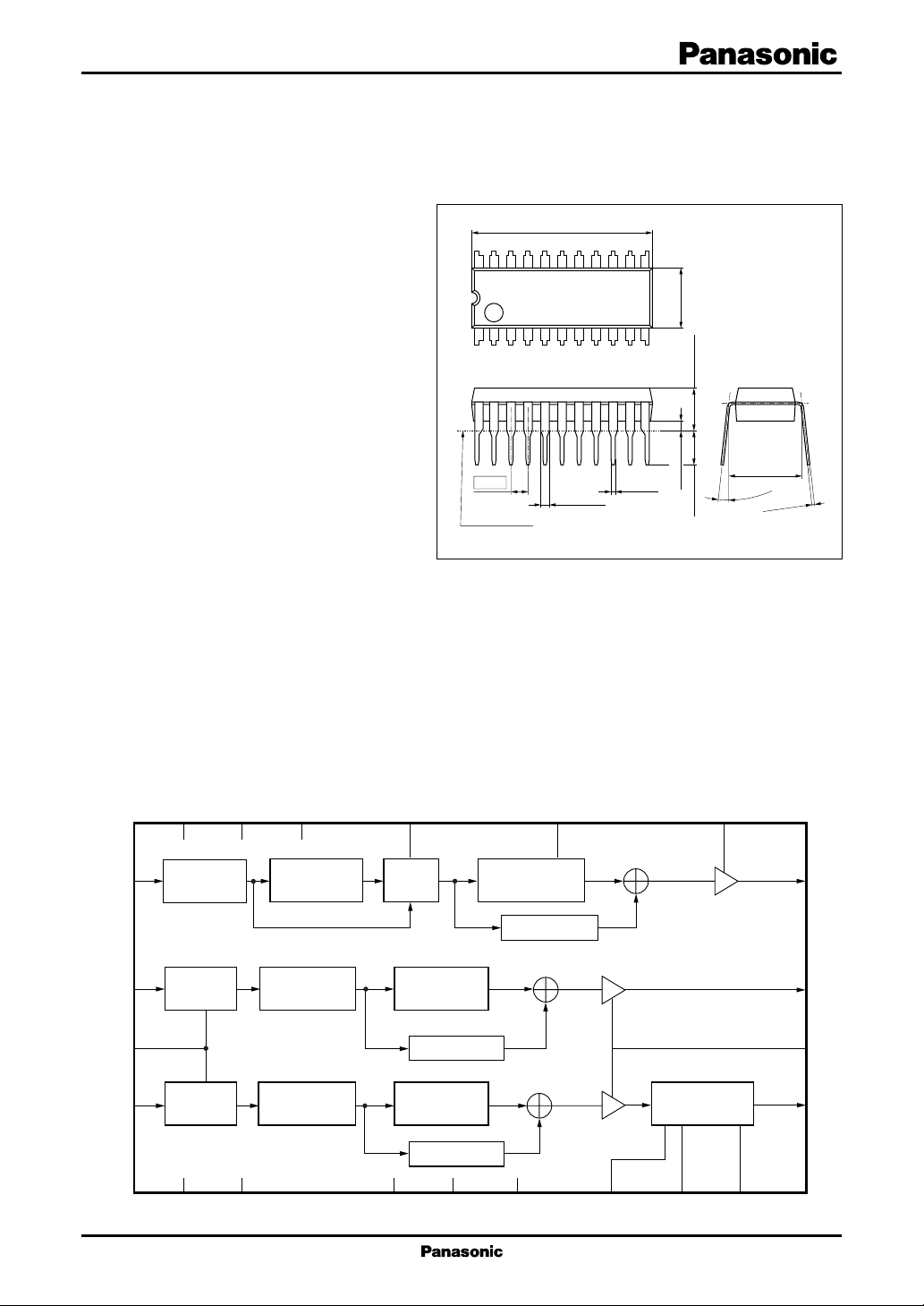
SDIP022-P-0300A
+0.10
– 0.05
■ Block Diagram
CC1
V
15
12
Y
U
C-pulse
V
IN
IN
IN
Sync chip
clamp
16
Pedestal
clamp
18
Pedestal
20
clamp
13
N.C.
17
21
CC2
V
N.C.
CC3
V
19
Delay line
Delay line
Delay line
Delay
switch
9
GND1
YDL
10
Correction
signal
generation
Delay line
Correction
signal
generation
Delay line
7
GND2
11
Correction signal
generation, white
side shoot erase
Delay line
5
GND3
YMCO
YMGA
14
8
Y
OUT
6
U
OUT
1
CTIG
POL
4
V
OUT
Red gamma
correction
22
VGA
2
3
VSL
1
Page 2

AN5385K ICs for T V
■ Pin Descriptions
Pin No. Description
Pin No. Description
1 CTI control pin
2 Red gamma folding point control pin
3 V-polarity switch pin
4 V-signal output pin
5 GND3 (V)
6 U-signal output pin
7 GND2 (U)
8 Y-signal delay time switch pin
9 GND1 (Y)
10 Y-signal delay time switch pin
11 Signal VM coring control pin
12 Y-signal input pin
13 N.C.
14 Signal VM control pin
15 V
CC1
(Y)
16 U-signal input pin
17 V
CC2
(U)
18 Clamp pulse input pin
19 V
CC3
(V)
20 V-signal input pin
21 N.C.
22 Red gamma control pin
■ Absolute Maximum Ratings
Parameter Symbol Rating Unit
Supply voltage V
Supply current I
2
Power dissipation
Operating ambient temperature
Storage temperature
Note)*1: Except for the operating ambient temperature and storage temperature, all ratings are for Ta = 25°C.
2: The power dissipation shown is the value for Ta = 70°C.
*
*
1
*
1
*
CC
CC
P
D
T
opr
T
stg
V
/ V
CC1
I
I
I
CC2
CC1
CC2
CC3
/ V
CC3
10.0 V
25.0 mA
25.0
25.0
750 mW
−20 to +70 °C
−55 to +150 °C
■ Recommended Operating Range
Parameter Symbol Range Unit
Supply voltage V
Note) On/off for V
Be careful for static electricity damage of pin 6.
CC1
/ V
CC2
and V
should be done simultaneously.
CC3
■ Electrical Characteristics at Ta = 25°C
Parameter Symbol Conditions Min Typ Max Unit
DC characteristics
Circuit current 1 I
Circuit current 2 I
Circuit current 3 I
Circuit voltage 1 V
Circuit voltage 2 V
2
CC1
CC2
CC3
3−5
4−5
CC1
V
V
V
V
V
/ V
CC1
CC1
CC1
CC1
CC1
CC2
= V
= V
= V
= V
= V
/ V
CC2
CC2
CC2
CC2
CC2
CC3
= V
= V
= V
= V
= V
8.1 to 9.9 V
= 9.0 V 11 14 17 mA
CC3
= 9.0 V 13 16 19 mA
CC3
= 9.0 V 14 17 20 mA
CC3
= 9.0 V 4.0 4.5 5.0 V
CC3
= 9.0 V 4.0 4.5 5.0 V
CC3
Page 3

ICs for TV AN5385K
■ Electrical Characteristics at Ta = 25°C (continued)
Parameter Symbol Conditions Min Typ Max Unit
DC characteristics (continued)
Circuit voltage 3 V
Circuit voltage 4 V
Circuit voltage 5 V
Circuit voltage 6 V
Circuit voltage 7 V
Y-system
output gain G
Y
OUT
I/O delay time 11 T
I/O delay time 12 T
I/O delay time 21 T
I/O delay time 22 T
V
= V
= V
6−7
8−9
12−9
16−7
20−5
Y
CC1
CC2
V
= V
CC1
CC2
V
= V
CC1
CC2
V
= V
CC1
CC2
V
= V
CC1
CC2
YIN: 2 MHz, 1.0 V[p-p] Sine wave −2.0 0.0 2.0 dB
= 9.0 V 2.5 3.0 3.5 V
CC3
= V
= 9.0 V 5.0 5.5 6.0 V
CC3
= V
= 9.0 V 3.2 3.6 4.0 V
CC3
= V
= 9.0 V 5.4 6.0 6.6 V
CC3
= V
= 9.0 V 5.4 6.0 6.6 V
CC3
input, YDL = 9.0 V, VMCO = 2.0 V
VMGA = 2.0 V
YIN: 500 kHz, 0.3 V[p-p] Sine wave 200 280 360 ns
Y11
input, YDL = 0.0 V, VMCO = 2.0 V
VMGA = 2.0 V
YIN: 2 MHz, 0.3 V[p-p] Sine wave 200 280 360 ns
Y12
input, YDL = 0.0 V, VMCO = 2.0 V
VMGA = 2.0 V
YIN: 500 kHz, 0.3 V[p-p] Sine wave 500 600 700 ns
Y21
input, YDL = 9.0 V, VMCO = 2.0 V
VMGA = 2.0 V
YIN: 2 MHz, 0.3 V[p-p] Sine wave 500 600 700 ns
Y22
input, YDL = 9.0 V, VMCO = 2.0 V
VMGA = 2.0 V
Coring characteristics 1 e
Coring characteristics 2 ∆e
Signal VM characteristics 1 e
Signal VM characteristics 2 ∆e
Y
frequency characteristics 1 ∆A
OUT
Y
frequency characteristics 2 ∆A
OUT
YIN: 2 MHz, 0.2 V[p-p] Sine wave 0.2 2.3 4.4 dB
co1
input, YDL = 9.0 V, VMGA = 4.0 V
VMCO: 2.0 V
YIN: 2 MHz, 0.2V[p-p] Sin wave 0. 4 2.4 4.4 dB
co
input, YDL = 9.0 V, VMGA = 4.0 V
VMCO: 4.0 V
YIN: 2 MHz, 1.0 V[p-p] Sine wave 1.0 2.5 4.0 dB
VM1
input, YDL = 9.0 V, VMCO = 3.0 V
VMGA = 3.0 V
YIN: 2 MHz, 1.0 V[p-p] Sine wave 3.0 4.0 5.0 dB
VM
input, YDL = 9.0 V, VMCO = 3.0 V
VMGA = 4.0 V
Y
Y1
: Measure at 7 MHz point, −3.0 dB
OUT
0 dB: 1 MHz, YDL = 0.0 V
VMCO = 2.0 V, VMGA = 2.0 V
Y
Y2
: Measure at 7 MHz point, −3.0 dB
OUT
0 dB: 1 MHz, YDL = 9.0 V
VMCO = 2.0 V, VMGA = 2.0 V
3
Page 4

AN5385K ICs for T V
■ Electrical Characteristics at Ta = 25°C (continued)
Parameter Symbol Conditions Min Typ Max Unit
U-system
output gain G
U
OUT
UIN: 500 kHz, 0.5 V[p-p] Sine wave 5.0 6.0 7.0 dB
U
input, C-pulse = 0 V, CTIG = 2.0 V
CTI characteristics 1 e
UCTI1UIN
: 500 kHz, 0.5 V[p-p] Sine wave 5.0 6.0 7.0 dB
input, C-pulse = 0 V, CTIG = 3.0 V
CTI characteristics 2 ∆e
UCTIUIN
: 500 kHz, 0.5 V[p-p] Sine wave 2.4 3.3 4.2 dB
input, C-pulse = 0 V, CTIG = 4.0 V
U
frequency characteristics ∆a
OUT
U
U
: Measure at 3 MHz point, −3.0 dB
OUT
0 dB: 500 kHz, C-pulse = 0 V
CTIG = 2.0 V
V-system
V
output gain G
OUT
VIN: 500 kHz, 0.5 V[p-p] Sine 4.9 6.0 7.1 dB
V
wave input, C-pulse = 0 V
CTIG = 2.0 V, VGA = 3.0 V
VSL = 5.0 V, POL = 9.0 V
CTI characteristics 3 e
VCTI3VIN
: 500 kHz, 0.5 V[p-p] Sine 4.7 5.7 6.7 dB
wave input, C-pulse = 0 V
CTIG = 3.0 V, VGA = 3.0 V
VSL = 5.0 V, POL = 9.0 V
CTI characteristics 4 ∆e
VCTIVIN
: 500 kHz, 0.5 V[p-p] Sine 1.7 2.6 3.5 dB
wave input, C-pulse = 0 V,
CTIG = 4.0 V, VGA = 3.0 V
VSL = 5.0 V, POL = 9.0 V
V
frequency characteristics ∆a
OUT
V
V
: Measure at 3 MHz point, −3.0 dB
OUT
0 dB: 500 kHz, C-pulse = 0 V
CTIG = 2.0 V, VGA = 3.0 V
VSL = 5.0 V, POL = 9.0 V
YU relative delay time T
YIN: 500 kHz, 1.0 V[p-p], UIN: −63780 ns
YU
500 kHz, 0.5 V[p-p], YDL = 9.0 V
VMCO = 2.0 V, VMGA = 2.0 V
C-pulse = 0.0 V, CTIG = 2.0 V
YV relative delay time T
V
YIN: 500 kHz, 1.0 V[p-p] −16 27 70 ns
YV
: 500 kHz, 0.5 V[p-p]
IN
YDL = 9.0 V, VMCO = 2.0 V
VMGA = 2.0 V, CTIG = 2.0 V
C-pulse = 0.0 V, VGA = 3.0 V
VSL = 5.0 V, POL = 9.0 V
UV relative delay time T
UIN: 500 kHz, 0.5 V[p-p], −96 −10 76 ns
UV
VIN: 500 kHz, 0.5 V[p-p],
CTIG = 2.0 V, C-pulse = 0.0 V
VGA = 3.0 V, VSL = 5.0 V
POL = 9.0 V
4
Page 5

ICs for TV AN5385K
■ Electrical Characteristics at Ta = 25°C (continued)
Parameter Symbol Conditions Min Typ Max Unit
V-system (continued)
Red gamma e
VGS11VIN
: 500 kHz, 0.5 V[p-p] Sine wave −3.6 0.0 3.6 dB
bending point variation 11 input, C-pulse = 0 V, CTIG = 3.0 V
VGA = 5.0 V, VSL = 3.0 V
POL = 9.0 V
Red gamma ∆e
VGS1VIN
: 500 kHz, 0.5 V[p-p] Sine wave 2.5 6.0 9.5 dB
bending point variation 12 input, C-pulse = 0 V, CTIG = 3.0 V
VGA = 5.0 V, VSL = 5.0 V
POL = 9.0 V
Red gamma e
VGS21VIN
: 500 kHz, 0.5 V[p-p] Sine wave −3.6 0.0 3.6 dB
bending point variation 21 input, C-pulse = 0 V, CTIG = 3.0 V
VGA = 5.0 V, VSL = 3.0 V
POL = 0.0 V
Red gamma ∆e
VGS2VIN
: 500 kHz, 0.5 V[p-p] Sine wave 1.5 5.0 8.5 dB
bending point variation 22 input, C-pulse = 0 V, CTIG = 3.0 V
VGA = 5.0 V, VSL = 5.0 V
POL = 0.0 V
Red gamma control 11 e
VGE11VIN
: 500 kHz, 0.5 V[p-p] Sine wave 4.5 5.5 6.5 dB
input, C-pulse = 0 V, CTIG = 3.0 V
VGA = 3.0 V, VSL = 3.0 V
POL = 9.0 V
Red gamma control 12 ∆e
VGE1VIN
: 500 kHz, 0.5 V[p-p] Sine wave 2.5 6.0 9.5 dB
input, C-pulse = 0 V, CTIG = 3.0 V
VGA = 5.0 V, VSL = 3.0 V
POL = 9.0 V
Red gamma control 21 e
VGE21VIN
: 500 kHz, 0.5 V[p-p] Sine wave 4.5 5.5 6.5 dB
input, C-pulse = 0 V, CTIG = 3.0 V
VGA = 3.0 V, VSL = 3.0 V
POL = 0.0 V
Red gamma control 22 ∆e
VGE2VIN
: 500 kHz, 0.5 V[p-p] Sine wave 1.5 5.0 8.5 dB
input, C-pulse = 0 V, CTIG = 3.0 V
VGA = 5.0 V, VSL = 3.0 V
POL = 0.0 V
• Design reference data
Note) The characteristics listed below are theoretical values based on the IC design and are not guaranteed.
Parameter Symbol Conditions Min Typ Max Unit
Y
supply voltage variation ∆e
OUT
Output DC level difference between 0.8 1.2 1.6 V
YIVcc
VCC (max.) and VCC (min.)
U
supply voltage variation ∆e
OUT
Output DC level difference between 0.4 0.8 1.2 V
UIVcc
VCC (max.) and VCC (min.)
V
supply voltage variation ∆e
OUT
Output DC level difference between 0.4 0.8 1.2 V
VIVcc
VCC (max.) and VCC (min.)
5
Page 6

AN5385K ICs for T V
■ Terminal Equivalent Circuits
Pin No. Equivalent circuit Description
1 CTI control pin:
9V(V
)
CC3
1
U-system V-system
3 V 3 V
16 kΩ
16 kΩ
16 kΩ
• Varies the CTI correction gain
2 V: Correction off
3 V: Correction amount center (approx. 6 dB)
4 V: Correction amount maximum (approx. 12 dB)
16 kΩ
50 µA
50 µA
• Recommended use range: 2 V to 4 V
2 Red gamma folding point control pin:
9 V (V
CC3
2
)
50 µA
20 kΩ 20 kΩ
• Varies the red gamma correction slice level
3 V: The folding point comes closest to the pedestal
5 V: The folding point is kept farthest from the
pedestal
4 V
• Recommended use range: 3 V to 5 V
3 V-polarity changeover pin:
9 V (V
)
CC3
50 µA
50 µA
• Changes over the input/output polarity of V-signal
Threshold value: 4.5 V
0 V: negative polarity
3
20 kΩ160 kΩ
3.8 V
9 V: positive polarity
4 V-signal output pin:
9 V (V
)
CC3
50 µA
4
50 µA
• To output the V-signal in which a correction signal
has been added to V-signal (R−Y) input from pin 20
• Output level: 1.0 V[p-p]
(where, 0.5 V[p-p] of U-signal input)
6
Page 7

ICs for TV AN5385K
■ Terminal Equivalent Circuits (continued)
Pin No. Equivalent circuit Description
5 GND3 pin:
• GND pin of V-system
6 U-signal output pin:
50 µA
6
9 V (V
CC2
)
• To output U-signal output in which a correction
signal has been added to U-signal (B−Y) input from
pin 16
50 µA
• Output level: 1.0 V[p-p]
(where, 0.5 V[p-p] of U-signal input)
7 GND2 pin:
• GND pin of U-system
8 Y-signal output pin:
• To output Y-signal in which a correction signal has
)
been added to the Y-signal inputted from pin 12
50 µA
9 V (V
CC1
8
• Output level: Synchronous negative 1.0 V[p-p]
50 µA
(where, 1.0 V[p-p] of Y-signal input)
9 GND1 pin:
• Y-system GND pin
9 V (V
)
10 Y-signal delay time changeover pin:
CC1
• Changes over Y-signal delay time
10
100 kΩ
Threshold voltage: 0.7 V
9 V: Total 600 ns delay
0 V: Total 280 ns delay
11 Signal VM coring control pin:
9 V (V
CC3
)
• To control VM signal coring volume
2 V: No coring
11
20 kΩ
3 V
20 kΩ
50 µA
4 V: Maximum coring (approx. 8%)
• Recommended usable range: 2 V to 4 V
7
Page 8

AN5385K ICs for T V
■ Terminal Equivalent Circuits (continued)
Pin No. Equivalent circuit Description
12 Y-signal output pin:
9 V (V
CC1
)
• To input video brightness signal
4.2 V
12
50 µA
• Input level:
10 µA
Synchronous negative: 1.0 V[p-p]
• Recommended use method:
Add a coupling capacitor (2.2 µ) to the input
signal in series.
13 N.C. pin:
• Ground
14 Signal VM control pin:
9 V (V
CC1
)
• To control correction gain of signal VM
2 V: correction off
14
16 kΩ
16 kΩ
50 µA
3 V
4 V: Maximum correction (approx. 6 dB)
• Recommended use range: 2 V to 4 V
15 Power supply pin (Y-system):
15
Operating supply voltage range:
9 V (allowance: ±10%)
16 U-signal input pin:
9 V (V
CC2
)
• To input the U-signal (B−Y) of color difference.
500 Ω500 Ω
16
CLP
25 µA
• Input level: 0.5 V[p-p]
17 Power supply pin (U-system):
17
Operating supply voltage range:
9 V (allowance: ±10%)
8
Page 9

ICs for TV AN5385K
■ Terminal Equivalent Circuits (continued)
Pin No. Equivalent circuit Description
18 Clamp pulse input pin:
19 Power supply pin (V-system):
9 V (V
18
CC2
)
50 µA
• To input a clamp pulse. Input SCP or H-sync
signal of 0 V to 5 V
SCP H-sync signal
3.5 V
4.7 V
2.4 V
Threshold voltage: 3.5 V
5.0 V
19
Operating power supply range:
9 V (allowance: ±10%)
20 V-signal input pin:
9 V (V
20
CC2
)
• To input the V-signal (R−Y) of color difference
500 Ω500 Ω
CLP
25 µA
• Input level: 0.5 V[p-p]
21 N.C. pin:
• Ground
22 Red gamma control pin:
9 V (V
CC3
)
50 µA
20 kΩ 20 kΩ
• To control correction gain of red gamma
3 V: Off
22
4 V
5 V: Maximum
• Recommended use range: 3 V to 5 V
9
 Loading...