

Page 1

ICs for TV
AN5367FB
NTSC video, chroma, and deflection signal processing circuit
■ Overview
The AN5367FB is an IC to demodulate the NTSC
composite signal. It is possible to control the all functions by the I
2
C bus. The use of flat package allows a space
saving in sets design.
■ Features
• Luminance signal processing
• Incorporating 3.58 MHz trap
• Black side gradation control is possible by black expansion circuit
• Adopting delay line aperture control
• Color signal processing
• Incorporating band-pass filter
• Incorporating ACC filter
• Deflection signal processing
• Stable sync. signal generation by the use of double
AFC circuit and countdown circuit
• Vertical directional screen position is adjustable
• Others
• Incorporating 3-input composite signal changeover
SW
• DAC output for adjusting sound volume and screen
height
14.0±0.3
12.0±0.2
36 25
37
48
112
(1.6)
0.80
Seating plane
0.35
QFP048-P-1212
+0.10
– 0.05
Unit: mm
24
(1.6)
12.0±0.2
14.0±0.3
13
(1.0)
– 0.05
+0.10
1.95±0.200.1±0.1
0.15
0° to 10°
0.5±0.2
■ Applications
• Color televisions and combined CTV/VCR set
1
Page 2
AN5367FB ICs for TV
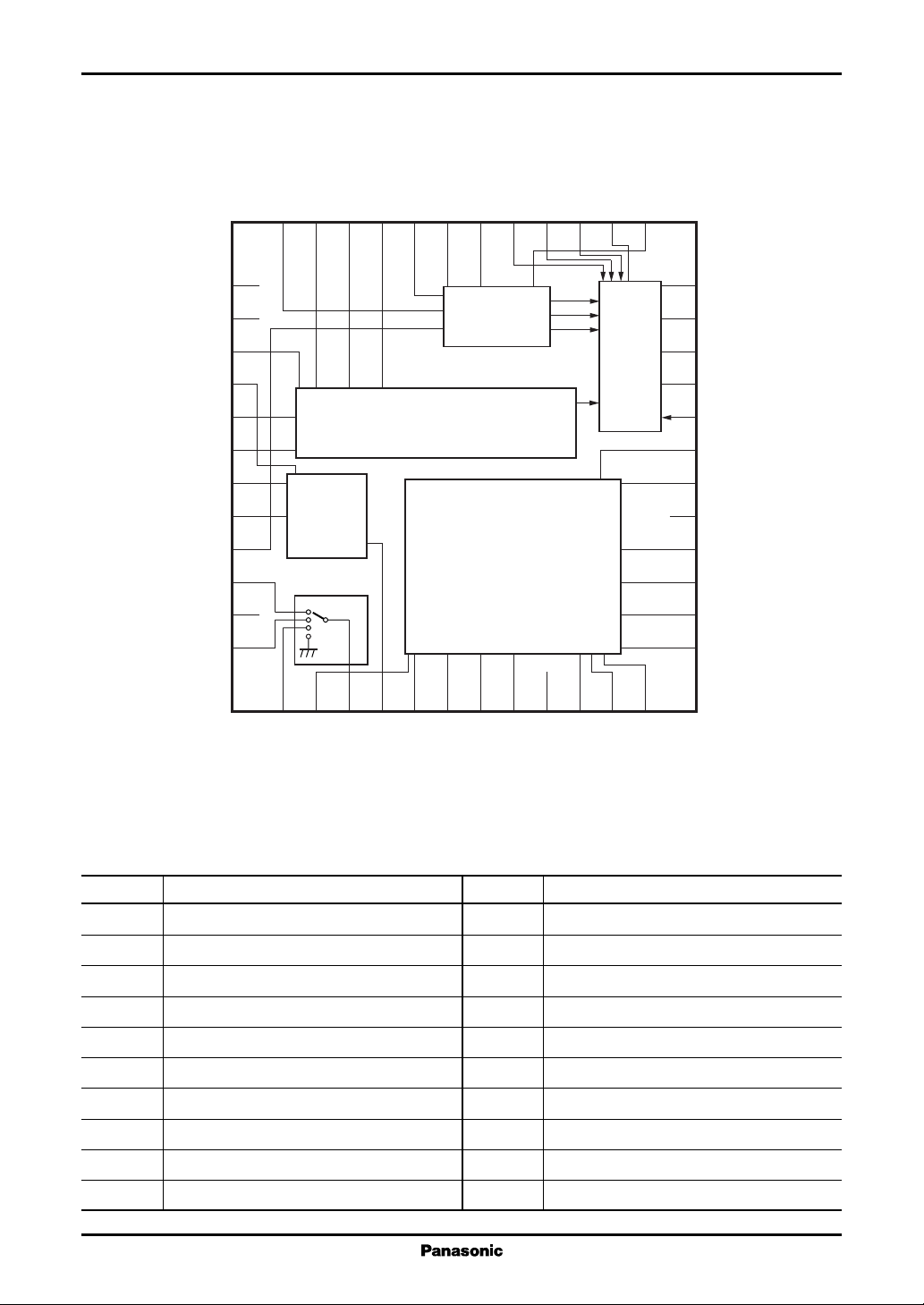
■ Block Diagram
C in
BL det.
BL start
ABL/ACL
Killer filter
SC out
APC filter
OSD-R in
OSD-G in
OSD-B in
Spot killer
FSC
36
35
34
33
32
31
30
29
28
27
26
25
V
CCREF
V
(9 V)
CC1
P clamp
DAC1 (V height)
Y in
APL det.
SCL
SDA
Killer out
Video3
(5 V)
V
CC2
Video2
37
38
39
40
41
42
43
44
45
46
47
48
1
Video1
Mute
2
2
I
SW
SYNC
V
C
3
Video out
4
DAC2 (sound)
Video
5
in
SYNC
V
6
in
H
Chroma
SYNC
7
Hold down ref.
Sync.
8
L det. out
9
10
V out
GND (Jungle)
RGB
11
X-ray
12
H OSC
24
23
22
21
20
19
18
17
16
15
14
13
Limiter
R out
G out
B out
Y
S
H out
BLK in
GND (main)
FBP in
L det. filter
H V
(6.2 V)
CC
H AFC1
■ Pin Descriptions
Pin No. Description
1 Video signal input pin 1
2 Vertical signal clamp pin
3 Video signal output pin
4 DAC output pin 1
5 Vertical sync. separation input pin
6 Horizontal sync. separation input pin
7 Hold down reference voltage pin
8 Lock detection output pin
9 GND pin (sync. system)
10 Vertical pulse output pin
2
Pin No. Description
11 Hold down input pin
12 Horizontal oscillation pin
13 Horizontal AFC1 filter pin
14 Horizontal stabilized power supply pin (6.2 V)
15 Lock detection filter pin
16 FBP input pin
17 GND pin
18 Blanking pulse input pin
19 Horizontal pulse output pin
20 YS input pin
Page 3
ICs for TV AN5367FB
■ Pin Descriptions (continued)
Pin No. Description
Pin No. Description
21 B output pin
22 G output pin
23 R output pin
24 Output limiter pin
25 Chroma oscillator pin
26 Spot killer pin
27 External B input pin
28 External G input pin
29 External R input pin
30 Chroma APC filter pin
31 Subcarrier output pin
32 Killer filter pin
33 ABL/ACL input pin
34 Black extension start adjusting pin
■ Absolute Maximum Ratings
Parameter Symbol Rating Unit
35 Black level detection filter pin
36 Chroma signal input pin
37 V
38 Power supply pin (V
reference voltage pin (9.6 V)
CC1
: 9 V)
CC1
39 Capacitor pin for Y clamp
40 DAC output pin 2
41 Y signal input pin
42 APL detection filter pin
43 SCL pin (for I2C bus)
44 SDA pin (for I2C bus)
45 Killer output pin
46 Video signal input pin 3
47 Power supply pin (V
CC2
: 5 V)
48 Video signal input pin 2
Supply voltage V
Supply current I
Power dissipation
Operating ambient temperature
Storage temperature
Note)*1 : Except for the operating ambient temperature and storage temperature, all ratings are for Ta = 25°C.
2 : The power dissipation shown is the value for Ta = 70°C.
*
*2
*1
*1
CC
CC
V
CC1 (38)
V
CC3 (47)
I
38
I
47
I
14
I
37
P
D
T
opr
T
stg
9.9 V
5.5
47 mA
31
13
5
775 mW
−20 to +70 °C
−55 to +150 °C
■ Recommended Operating Range
Parameter Symbol Range Unit
Supply voltage V
Supply current I
CC1
V
CC2
14
I
37
8.55 to 9.45 V
4.75 to 5.25
6.0 to 12 mA
1.0 to 4.5
3
Page 4
AN5367FB ICs for TV
■ Electrical Characteristics at Ta = 25°C
Parameter Symbol Conditions Min Typ Max Unit
SW and power supply
Circuit current 1 (I
)I
CC1
(9 V system) V
Circuit current 2 (I
)I
CC2
(5 V system) V
9.6 V reference voltage V
Operating resistance R
Zener maximum current I
SW circuit gain G
Frequency characteristics f
Crosstalk CT f = 1 MHz, input signal 0.7 V[p-p], −50 dB
Clamp current I
1
Total gain G
Y signal processing
Video input pin voltage V
Y typical output E
Video voltage gain relative ratio ∆GYAs same as the above, G/R, B/R −1.0 0 +1.0 dB
Video voltage gain G
Video frequency characteristics f
Picture quality variable range 1 G
Contrast ratio G
Brightness variable range BR Input: Without input, cut-off: max. , 2.15 2.40 2.80 V
Typical pedestal voltage PL
DC restoration ratio 1 T
RGB output BLK level Y
Black level correction amplitude 1 V
Note) Unless otherwise specified, refer to " • Typical conditions for testing" for the conditions of I2C bus and each pin.
No signal input, I14 = 8 mA, 28 36 43 mA
38
= 9 V,V
CC1
No signal input, I14 = 8 mA, 18 23 28 mA
47
= 9 V,V
CC1
I37 = 2.4 mA 9.0 9.6 10.2 V
37
I37 = 1.0 mA to 5.0 mA 0 11 30 Ω
37
Largest possible sink current 5 mA
VD
f = 1 MHz, 0.7 V[p-p] 4.9 5.9 6.9 dB
SW
Attenuation amount at 7 MHz with f =−3 −1.3 dB
SW
CC2
CC2
= 5 V
= 5 V
1 MHz as reference
sine wave
, I46 , Sink current of each input pin, when 6 10 14 µA
I
applying 3 V to pin 1, pin 46 and pin 48
48
Gain dispersion from each input to output −19 0 +19 %
TOTAL
VCC: Typ., input pin voltage measure- 1.1 1.5 1.9 V
41
ment
Input 2 V[p-p] stair steps 2.6 3.2 3.8 V[0-p]
OSTD
Input 2 V[p-p] stair steps, contrast: typ. 1.7 2.1 2.5 V[0-p]
Y
Attenuation amount at 6 MHz with −5.0 −2.0 dB
Y
f = 1 MHz as reference
Input 0.2 V[p-p], sine wave f = 2.5 MHz, 5.9 9.0 11.4 dB
S1
sharpness: typ./min.
Input 2 V[p-p] stair steps, 6 9 12 dB
C
contrast: max./min.
brightness: min. to max. , pedestal level
measurement
Input: Without input 1.95 2.60 3.10 V
STD
Input 2.0 V[p-p] total white, APL 10% 94 10 0 106 %
DC1
to 90%, DC restoration ratio correction:
Off (pin 42: 0 V)
BLKVCC
BL1
: typ. 1.0 1.5 2.0 V
Input signal: Total black, black level −100 0 +100 mV
detection pin: external RC → 9 V,
BL start = 20 kΩ
4
Page 5
ICs for TV AN5367FB
■ Electrical Characteristics at Ta = 25°C (continued)
Parameter Symbol Conditions Min Typ Max Unit
Y signal processing (continued)
Black level correction amplitude 2 V
Black level correction amplitude 3 V
Black level correction amplitude 4 V
Y signal delay time t
Sub-contrast adjustment range 1 E
Sub-contrast adjustment range 2 E
Trap attenuation amount G
Delay line ∆t
ACL variable range ∆ACL Pin 33 7.5 V → 2.5 V, stair step 2 V[p-p] 12 20 28 %
ABL variable range ∆ABL Without input, pin 33: 4.5 V → 2.5 V, 0.4 0 . 6 0.8 V
Color signal processing
ACC characteristics 1 ACC1 Color bar input: 6 dB up, 0.9 1.0 1.1 Times
ACC characteristics 2 ACC2 Color bar input: 20 dB down, 0.7 0.9 1.1 Times
Color killer tolerance 1 e
Color difference output (B−Y) 1 e
Color difference output (B−Y) 2 e
Color residue e
Chroma contrast C
Free-running frequency f
APC pull-in range 1 f
Tint center data TC Rainbow signal, tint data at which 15 1D 25 H
Note) Unless otherwise specified, refer to " • Typical conditions for testing" for the conditions of I2C bus and each pin.
Input signal: Total black, black level 0.46 0.80 1.14 V
BL2
detection pin: 3 V, BL start = 20 kΩ
Adjust output amplitude to 0.8 V[p-p], 0.10 0.25 0.40 V
BL3
black level detection pin: 9 V → external
RC, BL start = 20 kΩ
Adjust output amplitude to 2.0 V[p-p], − 0.1 0 +0.1 V
BL4
black level detection pin: 9 V → external
RC, BL start = 20 kΩ
Input 2.0 V[p-p] stair step, B.P.F. SW: 330 410 490 ns
D1
On, trap SW: On, measurement of time
delay between input and output
Sub-contrast typ. → min., −40 −30 −22 %
OADJ1
input: 2 V[p-p] stair step
Sub-contrast typ. → max., 35 46 55 %
OADJ2
input: 2 V[p-p] stair step
f = 3.579545 MHz, trap on/off 23 dB
TRAP
Difference of amount of delay between 90 120 150 ns
D
B.P.F. on/off
pedestal voltage of RGB output
(R−Y) output measurement,
burst typical input = 150 mV[p-p]
(R−Y) output measurement,
burst typical input = 150 mV[p-p]
Level at which demodulation output does −53 −43 −34 dB
K1
not appear when color bar input level is
being attenuated. Typical input level: 0 dB
Color bar input, color: typ., tint: Center 1.55 2.00 2.45 V[0-p]
O1
Color bar input, color: max., tint: Center 2.85 3.7 4.5 V[0-p]
O2
Color bar input, color: min. 15 60 mV
LC
Color bar input, contrast: min. → max. 5.2 8.2 11.2 dB
CONT
For f0 of typical sample, −300 0 +300 Hz
C0
f0 = 3.579545 MHz
Color bar: Typical input, B.P.F.: On ±450 ±600 Hz
APC
B−Y output becomes typical.
5
Page 6

AN5367FB ICs for TV
■ Electrical Characteristics at Ta = 25°C (continued)
Parameter Symbol Conditions Min Typ Max Unit
Color signal processing (continued)
Tint variable range ∆θ Tint = min. to max. ±30 ±45 deg
Demodulation output ratio R/B R/B Rainbow input 0.76 0.96 1.15 Times
Demodulation output ratio G/B G/B Rainbow input 0.27 0.36 0.45 Times
Demodulation angle ∠R ∠R Reference is ∠B 96 104 112 deg
Demodulation angle ∠G ∠G Reference is ∠B 225 235 245 deg
Demodulation output residual carrier
CW output DC level 1 V
CW output DC level 2 V
CW Out output level A
High-level killer output KILHPin 45 voltage measurement, V32 = 5.5 V
Low-level killer output KILLPin 45 voltage measurement, V32 = 4 V
Killer output open KIL
RGB processing
RGB output DC difference voltage ∆PL
RGB output limit level V
External RGB input clip level 1 E
External RGB input clip level 2 E
External RGB input clip level ∆E
difference clip level difference among R, G and
External RGB gain G
External RGB frequency f
characteristics 0.3 V[p-p], sine wave, reference: 1 MHz,
Internal/external pedestal ∆PL
difference voltage
Y
threshold level YSPin 20 voltage at which inside and 1.1 1.6 2.1 V
S
Cut-off variable range ∆CO Without input, cut off: min. to max. 1.2 1.5 1.8 V
Drive variable range ∆DR Input: staircase, 2.0 V[p-p], drive: min. 5 7 9 dB
Note) Unless otherwise specified, refer to " • Typical conditions for testing" for the conditions of I2C bus and each pin.
A
FSCfSC
31(1)
31(2)
CW
OP
1
LIM
G1
G2
G1YS
EXTYS
EXT
2
component of demodulation output 20 50 mV[p-p]
Subcarrier output: Off 1.4 1.9 2.4 V
Subcarrier output: On 5.6 6.1 6.6 V
Output level of f
SC
250 350 500 mV[p-p]
4.0 4.6 V
0.4 1.0 V
At VV mode, I45 measurement, −10+1 µA
V32 = 4 V or 5.5 V
∆V = VR −VG , VG −VB , VB −VR , −300 0 +300 mV
burst input only, cut off: min.
Input: 2.0 V[p-p], total white, contrast: 6.6 6.9 7.2 V
max., cut off: max., bright: max.
YS: H, contrast: max., difference from 2.2 2.6 3.0 V
internal pedestal voltage, cut off: min.,
drive: typ.
YS: H, contrast: min., difference from 1.1 1.6 2.1 V
internal pedestal voltage, cut off: min.,
drive: typ.
: H, contrast: max., external input −300 0 +300 mV
B channel
: H, contrast: max., input voltage: 1.6 2 .3 3.0 Times
0.3 V[p-p], sine wave, 1 MHz
YS: H, contrast: max., input voltage: −4.8 −1.8 dB
attenuation amount at 7 MHz
Burst input only, YS: high/low 50 250 600 mV
outside change over
to max.
6
Page 7
ICs for TV AN5367FB
■ Electrical Characteristics at Ta = 25°C (continued)
Parameter Symbol Conditions Min Typ Max Unit
Horizontal signal processing
Horizontal stabilized power supply V
voltage input current I14 = 8 mA
Horizontal stabilized power supply I
maximum current supply is stabilized
Horizontal stabilized power supply R
on-state resistance I14 = 6 mA to 13 mA
Horizontal output start voltage V
Horizontal output pulse duty τ
High-level horizontal output V
Low-level horizontal output V
Horizontal output free-running f
frequency is no horizontal sync. separation input
Hor. pull-in range f
Screen position fluctuation 1 H
Screen position fluctuation 2 H
Hold Down operation level V
High-level lock det. output LD
Low-level lock det. output LD
BLK-in input threshold voltage BLK
Vertical signal processing
Ver. out pulse width τ
High-level ver. out 1 V
High-level ver. out 2 V
High-level ver. out 3 V
Note) Unless otherwise specified, refer to " • Typical conditions for testing" for the conditions of I2C bus and each pin.
Pin voltage, when power supply pin 5.7 6.1 6.8 V
14
Maximum input current for which power 13 mA
14
On-state resistance, when input current 0 14 30 Ω
14
Horizontal stabilized power supply 4.5 5.2 V
FHS
voltage, when horizontal output pulse
becomes 1 V[p-p] or more. Do not
apply other power supply voltage.
Horizontal output pulse high level duty 46.9 50.0 53.1 %
HO
Horizontal output pulse high level 4.0 4.3 4.6 V
19H
Horizontal output pulse low level 0.2 0.5 V
19L
Horizontal output frequency, when there 15.45 15.73 16.05 kHz
HO
Frequency at which horizontal sync. ±500 ±600 Hz
HP
separation input frequency pulls in.
Sync. signal 0.57 V[p-p].
Phase change of horizontal sync. signal −1.70 −2.12 −2.55 µs
POS1
and FBP, H-center (0A): 67 → 60
Phase change of horizontal sync. signal 1.97 2.46 3.14 µs
POS2
and FBP, H-center (0A): 67 → 6F
Voltage at which X-ray input pin voltage 5.9 6.2 6.5 V
HD
holds down. Hold down pin reference
voltage: 6.2 V
At horizontal AFC unlocked, 4.5 V
H
RL = 56 kΩ
At horizontal AFC locked, 0.7 V
L
RL = 56 kΩ
Pin 18 threshold voltage (BLK is applied 1.7 2.2 2.7 V
ST
to RGB output stage only)
Pulse width at horizontally/vertically 610 640 670 µs
VO
synchronized state
Vertical output pulse high level 4.0 4.3 4.6 V
10H1
pin 10: open
Vertical output pulse high level 3.75 4.10 4.60 V
10H2
pin 10: − 0.2 mA
Vertical output pulse high level 3.3 3.9 4.6 V
10H3
pin 10: − 0.5 mA
7
Page 8

AN5367FB ICs for TV
■ Electrical Characteristics at Ta = 25°C (continued)
Parameter Symbol Conditions Min Typ Max Unit
Vertical signal processing (continued)
Low-level ver. out V
free-running frequency f
V
OUT
Vertical pull-in range f
V
position shift V
OUT
I2C processing
SCL, SDA input threshold voltage
V
SCL
Sink capability at ACK ACK I = 3 mA when pull-up resistor is 1.6 kΩ 0.4 V
High level DAC output 1 V
High level DAC output 2 V
Low level DAC output 1 V
Low level DAC output 2 V
Note) Unless otherwise specified, refer to " • Typical conditions for testing" for the conditions of I2C bus and each pin.
Vertical output pulse low level 0 0.3 V
10L
Ver. out frequency, when there are no 58 60 62 Hz
VO
hor. and ver. sync. signals input.
Sync. input: 2 V[p-p], measurement should
VP
56 64 Hz
be conducted from not pulled in state.
V position: min. → max. 31 H
POS
, V
SDA
Pin 4 output DC voltage, 0D = 7F 8.25 8.75 9.25 V
4H
Pin 40 output DC voltage, 0C = 7F 4.5 5.0 5.5 V
40H
Pin 4 output DC voltage, 0D = 00 0.60 0.90 1.20 V
4L
Pin 40 output DC voltage, 0C = 00 0 0.1 0.2 V
40L
1.5 3.0 V
• Design reference data
Note) The characteristics listed below are theoretical values based on the IC design and are not guaranteed.
Parameter Symbol Conditions Min Typ Max Unit
SW power supply
Reference voltage-temperature ∆V
/TaI37 = 2.4 mA, T = −20°C to +70°C −1.4 −1.8 −2.2 mV/°C
37
characteristics
SW input dynamic range SW
Input clamp voltage V
1
1 V[p-p] is reference (0 dB), 6 dB
D
V
= 9 V, V
CC1
, V
, Without input, pin 1, pin 46 and pin 48 1.8 2.2 2.6 V
46
V
voltage
48
CC2
= 5 V
SW output voltage V3Without input, pin 3 voltage 2.6 3.0 3.4 V
SW output−Y input V
−V41Without input, difference voltage 1.0 1.2 V
3
DC difference voltage between pin 3 and pin 41
SW output−H. Sync. V
−V6Without input, difference voltage 1.0 1.2 V
3
DC difference voltage between pin 3 and pin 6
SW output−V. Sync. V
−V5Without input, difference voltage 1.0 1.2 V
3
DC difference voltage between pin 3 and pin 5
Y signal processing
Video maximum output voltage E
Y signal input dynamic range Y
Brightness: max. 7.5 V
Omax
Input D range measurement, contrast: 4.0 V[p-p]
IN
typ., sub-contrast: typ.
Picture quality variable range 2 G
Input: 0.2 V[p-p], sine wave, f = 2.5 MHz, 13 dB
S2
sharpness: max./min.
8
Page 9

ICs for TV AN5367FB
■ Electrical Characteristics at Ta = 25°C (continued)
• Design reference data (continued)
Note) The characteristics listed below are theoretical values based on the IC design and are not guaranteed.
Parameter Symbol Conditions Min Typ Max Unit
Y signal processing (continued)
Contrast fluctuation with picture ∆A
quality control sharpness: max./min.
Brightness relative control ∆BR Same as the above G/R, B/R, 0.9 1 1.1 Times
sensitivity brightness: min. → max.
Black level correction starting V
point voltage
Video signal output supply voltage ∆E
dependency V
Output DC voltage ambient ∆E
temperature dependency T
Y S/N Y
Service SW operation 1 SRSW1Input: 2.0 V[p-p], stair step, service SW: 10 150 mV[p-p]
Service SW operation 2 SRSW
DC restoration ratio 2 T
Trap center frequency f
Delay amount of trap τ
Temperature characteristics of ∆G
trap attenuation amount T
Temperature characteristics of ∆f
trap frequency T
ACL start voltage ACL
ACL stop voltage ACL
ABL start voltage ABL
ABL stop voltage ABL
Color signal processing
Maximum color difference output e
Free-running frequency supply ∆f
voltage dependency V
VCO control sensitivity β Check change in oscillation frequency, 2.8 Hz/mV
Input: 2.0 V[p-p], stair step, −300 +300 mV[p-p]
SC
BL start external resistor: 20 kΩ53 IRE
BLSTA
/ Input: 2.0 V[p-p], stair step, output 0 0.25 V[p-p]/
O
amplitude change of VCC = ±5% V
CC
/ Pedestal level change ratio, when T
ODC
changes from 50°C to 75°C, contrast:
a
−1.8 mV/°C
a
max.,brightness: typ.
Input: 2.0 V[p-p], stair step, noise meter 53 55 dB
S/N
measurement, contrast: max., sharpness: min.
Measurement of output amplitude, when
SW is on.
Service SW: On, DC voltage measure- 3.8 4.3 4.8 V
2
ment at no-appearance of V
2.0 V[p-p], stair step, APL det. = 20 kΩ 120 %
DC2
Difference from f = 3.579545 MHz −70 +70 kHz
0TRAP
f = 0.5 MHz, comparison of delay 40 ns
TRAP
OUT
.
amount between trap on/off
/f = 3.579545 MHz, −20°C to +70°C23 dB
TRAP
a
/ −20°C to +70°C −50 +50 kHz
TRAP
a
Pin 33 voltage at which ACL starts to 7.1 V
STA
become effective
Pin 33 voltage at which ACL stops 2.9 V
STO
Pin 33 voltage at which ABL starts to 4.0 V
STA
become effective
Pin 33 voltage at which ABL stops 3.0 V
STO
Color bar input, brightness: min., 4.5 V[0-p]
Omax
color: max., pedestal to peak voltage
/VCC = ±5% −250 +250 Hz
CO
CC
when V
= 5.6 V to 5.8 V
APC
9
Page 10

AN5367FB ICs for TV
■ Electrical Characteristics at Ta = 25°C (continued)
• Design reference data (continued)
Note) The characteristics listed below are theoretical values based on the IC design and are not guaranteed.
Parameter Symbol Conditions Min Typ Max Unit
Color signal processing (continued)
Free-running frequency ambient ∆f
temperature dependency
Phase detection sensitivity µ {1/ (∆φ × β)} × 100 22.3 mV/deg
Phase hold characteristic ∆φ Change amount of tint, when f
Demodulation output frequency ∆f
characteristic becomes −3 dB
Demodulation output supply
voltage dependency color: typ.
Demodulation output ambient ∆e
temperature dependency
Tint Center shift ∆T
H.P.F. frequency characteristic f
H.P.F. group delay amount τ
Color killer tolerance 2 e
Chroma delay amount τ
C−Y/Y ratio C−Y/Y
RGB processing
Y output amplitude fluctuation ∆E
(trap on/off) fluctuation at trap on/off
Y output amplitude fluctuation ∆E
(B.P.F. on/off) fluctuation at B.P.F. on/off
Y output amplitude fluctuation
(sharpness) min. → max.
Spot killer operation V
Horizontal signal processing
Sync. separation clamp voltage V
Black out operation level V
Operating frequency at hold f
down down when X-ray input pin voltage is
BGP start position BGP
/TaAmbient temperature: −20°C to +70°C −2.9 Hz/°C
CO
is 1.6 deg/
SC
shifted by ±300 Hz 100 Hz
Frequency at which color output pin 1.1 MHz
−3
∆eO /VCCTint: typ., contrast: typ., VCC ±5%, 0 %
/TaTa = −20°C to +70°C, +25°C is typ. ±7 %
O
Change amount of tint center, when ±4 H
C
B.P.F. is used and not.
HPF
HPF
K2
CHO
OTRAP
OBPF
∆E
OSHARP
SPKVCC1
Gain at f = f
Group delay amount at f = f
SC
SC
B.P.F. on state −43 dB
Delay from pin 36 input to pin 21 output 375 ns
Color data, when C−Y/Y ratio becomes 1.0
2 V[p-p] staircase input, amplitude ±10 %
2 V[p-p] staircase input, amplitude ±10 %
2 V[p-p] staircase input, sharpness: ±5 %
voltage at which RB
output 7.6 V
RGB
−12 dB
140 ns
40 H
becomes high, when pin 26 voltage = 8.25 V
, V6Clamp voltage of sync. separation input 1.4 V
5
pin (pin 5 and pin 6)
Voltage at which Y output blacks out 6.3 V
BLOUT
when X-ray input pin voltage is raised
from 0 V
HD
Frequency of H
at the time of hold 16.3 16.4 16.8 kHz
OUT
raised from 0 V
Phase difference from rear edge of hor. 0.3 0.5 0.7 µs
STA
sync. to BPG at horizontal AFC loop on
10
Page 11

ICs for TV AN5367FB
■ Electrical Characteristics at Ta = 25°C (continued)
• Design reference data (continued)
Note) The characteristics listed below are theoretical values based on the IC design and are not guaranteed.
Parameter Symbol Conditions Min Typ Max Unit
Horizontal signal processing (continued)
BGP pulse width BGPWBGP width at horizontal AFC loop on 2.5 3.0 3.5 µs
FBP level 1 V
FBP level 2 V
FBP delay operating range τ
Horizontal oscillation frequency ∆f
temperature characteristics −20°C to +70°C
Vertical signal processing
V. BLK pulse width VBLK
I2C processing
Each DAC precision for 4-bit, DAC1 1LSB = {data (max.) − data (min.)}/ 0.1 1 1.9 LSB/
5-bit, 6-bit (2N−1) step
Each DAC precision for 7-bit, DAC2 1LSB = {data (max.) − data (min.)}/ 0.1 1 1.9 LSB/
7+1-bit, (40) excluded (2N−1) step
Each DAC precision for 7-bit, DAC3 1LSB = {data (max.) − data (min.)}/ −1 1 2 LSB/
7+1-bit, (40) only (2N−1) step
Each DAC precision for 7+1-bit DAC4 1LSB = {data (max.) − data (min.)}/ −9.25 −6.25 0 %
(7F → 80) (2N−1), sub address; 06, 07
AFC operation DC level at FBP input pin
FBP1
HBLK operation DC level at FBP input pin
FBP2
Range of normal operation, when 10.0 to 22.0 µs
FBP
1.4 2.0 2.2 V
0.3 0.7 1.1 V
delay amounts are being changed from
raise of H
Change in ambient temperature from ±100 Hz
HO/Ta
VBLK width at R,G,B out in 17.0 H
W
to FBP center.
OUT
horizontall/verticall synchronization
(
Change amount/total change amount) × 100
• Typical conditions for testing
1. Input signal
1) Video: 10-step staircase, 2.0 V[p-p]
2) Chroma: Color bar signal: Burst level 150 mV[p-p]
Rainbow signal: Burst level 150 mV[p-p]
3) Sync. signal: Video signal 1.5 V[p-p] to 2.5 V[p-p] for both horizontal and vertical sync. signal input
2
C bus conditions
2. I
Sub address Control Data (H) Sub address Control Data (H)
00 Color 40 08 Drive G 40
01 Tint 20 09 Drive B 40
02 Brightness 40 0A Y-adjust, H-center 67
03 Contrast 3F 0B Test, V-position 00
04 Sharpness 00 0C DAC1 40
05 Cut off R 00 0D DAC2 40
06 Cut off G 00 0E SW 50
07 Cut off B 00
11
Page 12

AN5367FB ICs for TV
■ Electrical Characteristics at Ta = 25°C (continued)
• Typical conditions for testing (continued)
3. State of each pin
Pin No. Symbol State
18 BLK in 0 V
20 Y
S
24 Limiter V
33 ABL/ACL 7.5 V
34 BL start 20 kΩ
35 BL det. V
38 V
CC1
42 APL det. 0 V
47 V
CC2
• Functions of SW controlled by I2C bus
Data-bit Functions of SW Contents
0E-D0 AV SW changeover 1. Composite signal changeover
0E-D1 D1 D0 Output Input Video1: Pin 1
0 0 Video1 Video2: Pin 48
0 1 Video2 Video3: Pin 46
1 0 Video3 Output : Pin 3
1 1 Mute 2. No output at mute
1.1 V
CC1
CC1
Applied from outside (9 V)
5 V
0E-D2 Chroma trap SW 1. Video circuit chroma trap changeover
(0 → without trap) (Y signal phase leads by about 40 ns at trap off
(1 → with trap) (through))
0E-D3 Chroma B .P.F. SW 1. Chroma circuit band-pass filter changeover
(0 → without B.P.F.) (Video signal delay amount varies according to
(1 → with B.P.F.) B.P.F. on/off)
0E-D4 EE/VV SW 1.
Tuner (EE) and VTR (VV) changeover
0E-D7 D7 D4 Killer out fSC out In principle change over by D4
0 0 Killer result Yes Tuner (EE): Killer result is output
0 1 Open No fSC is output
1 0 Killer result Yes VTR (VV): Killer result is not output
1 1 Open Yes fSC is not output
However, fSC is output if D7 = 1 even at VV.
Killer out: Pin 45, fSC out: Pin 31
0E-D5 SSW (service SW) 1. At service mode (no vertical scanning, white
(0 → normal) balance adjustment)
(1 → service mode) Vertical output pulse stops (DC about 4.3 V)
Y output off, chroma output small
0E-D6 BLK off SW 1. RGB output blanking (BLK) off changeover
(0 → normal) To be used when RGB output
(1 → output without BLK)
BLK
is required.
signal without
12
Page 13

ICs for TV AN5367FB
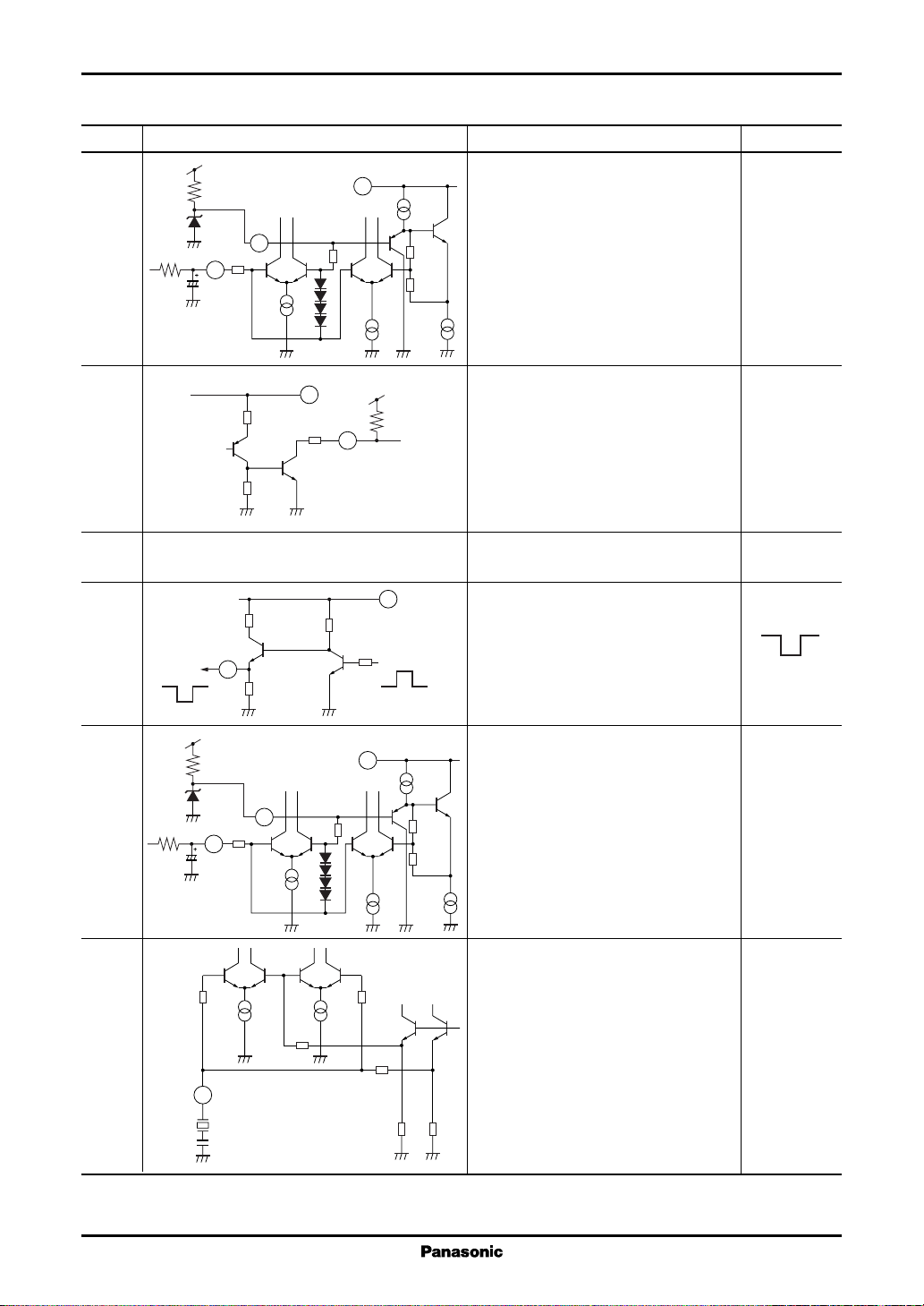
■ Terminal Equivalent Circuits
Pin No. Equivalent circuit Description Voltage
1 Video signal input pin 1: AC
200 Ω
200 Ω
1
1.25 kΩ
2.75 V
10 µA
10 µF
38
25 µA
V
CC1
9 V
• Video signal input pin
• Typical input 1.0 V[p-p]
• Input through capacitor, and sync. top
is clamped at 2.2 V
• Input video signal with low impedance
1.0 V[p-p]
2.2 V
2 Vertical signal clamp pin: AC
3 kΩ
2
30 kΩ
200 Ω
220 Ω
2.2 µA
50 kΩ
10 kΩ
10 kΩ
211 Ω
3 Video signal output pin: AC
200 Ω
3
50 Ω
400 Ω
4 DAC output pin 1: DC
12 V
100 µA
4
4 kΩ
200 Ω
200 Ω
1 kΩ
40 kΩ
100 µA
5
1.75
kΩ
20
µA
16 kΩ
400 Ω
1.75
kΩ
20
µA
16 kΩ
6
16 kΩ
1 µF
CV
0.1 µF
1200 pF
CH
400 Ω
5
6
RV
560 Ω
680 pF
RH
270 Ω
V
47
5 V
To ver.
count down
38
100 µA
38
1 kΩ
0 µA to
200 µA
47
To H sync. sep.
To V sync. sep.
1.3 V
CC2
• Peak clamp pin for separating vertical f = f
sync. signal
• Outputs signals inputted from pin 1,
pin 46 and pin 48
• Control of output signal is carried out
2
by I
C bus
• Recommended range of use is from
−2 mA to +2 mA
• Output voltage is adjustable in 128 0.95 V
stages (7-bit organization) by sub- to
address of I
2
C bus (0D). 8.75 V
• Recommended range of use is from
−70 µA to +70 µA
Pin 5: Vertical sync. separation input pin:
Pin 6: Horizontal sync. separation input pin:
•RV >RH so that slice level is made
deep for vertical sync. and shallow for
horizontal sync.
• Cutoff frequency determined by R
and CH shall be about 500 kHz.
•R → large, slice level becomes
deeper. (Weak in sync. compression)
•R → small, slice level is shallow.
(Weak in fluctuation such as V sag)
2.0 V[p-p]
AC
2 V[p-p]
H
V
3.0 V
13
Page 14
AN5367FB ICs for TV
■ Terminal Equivalent Circuits (continued)
Pin No. Equivalent circuit Description Voltage
100 Ω
12 V
6.2 V
11
10 µF
1 kΩ
7
100
µA
1 kΩ
µA
38
50 µA
65
kΩ
10
kΩ
25
µA
• Operates hold down by comparing 6.2 V
voltage inputted to pin 11
V
>V11: Normal operation
7
V7 <V11: Out of horizontal sync.
V7 +0.1 V<V11: Output with all BLK.
• Recommended range of use is from
50
3 V to 7 V
7 Hold down reference voltage pin: DC
760 Ω
8 Lock detection output pin: DC
47
5 kΩ
1.2 kΩ
5 V
56 kΩ
8
• Pin which outputs whether vertical 0.7 V or less
sync. signal of input and H
are at lock,
OUT
synchronizing. 4.5 V or more
• Recommended range of use is from at unlock
60 kΩ
0 mA to 0.2 mA
9 GND pin:
• Sync. system GND
10 Vertical pulse output pin: AC
200 Ω
10
43 kΩ
100 Ω
12 V
6.2 V
11
10 µF
1 kΩ
7
100
1 kΩ
µA
11 Hold down reference voltage pin: DC
760 Ω
50 kΩ
20 kΩ
25
µA
47
• Negative polarity, pulse width 10H
• Recommended range of use is from
1.8 V
0 V
38
50 µA
65
kΩ
10
kΩ
50
µA
− 0.7 mA to 0 mA
• Voltage in proportion to a hightension of CRT is applied.
4.3 V
0 V
12 Horizontal oscillation pin: AC
• Oscillates at 32fH ≅ 503 kHz by means f = 32f
CSB
503F38
270 Ω
12
220 pF (N750)
100
µA
435 Ω
200
µA
270 Ω
300 Ω
10
kΩ
of ceramic oscillator element approx.
• Makes horizontal and vertical pulse
by internal countdown circuit of IC.
10
kΩ
14
(
503 kHz
H
)
Page 15

ICs for TV AN5367FB
■ Terminal Equivalent Circuits (continued)
Pin No. Equivalent circuit Description Voltage
13 Horizontal AFC1 filter pin: DC
Duty 50%
1.5 V
14
27 kΩ
200 Ω200 Ω
R1
4.3 V
2.2
kΩ
4.4
kΩ
27 kΩ
2.2
kΩ
• Charges and discharges the capacitor typ. 4.3 V
connected to pin 13 after comparing
the phase of horizontal sync. signal
and pulse inside IC.
• R1, R2, C1 and C2 are lag-lead filter
4.4
kΩ
for AFC1.
13
12 V
10 µF
2.2 kΩ
760 Ω
R2
C2
C1
0.018 µF
14
47 µF0.01 µF
Hor. sync.
1 000 µA
14 Horizontal stabilized power supply pin: DC
200 µA
6.1 V
Hor.
OSC
f
H
Horizontal
β curve
V
13
• Stabilized power supply for horizontal 6.1 V
circuit.
A constant voltage circuit is inside.
• Recommended range of use is from
6 mA to 12 mA
15 Lock detection pin: DC
200 Ω
200 Ω
10 kΩ
47
• Detects phase of horizontal sync.
In synchronization
signal and horizontal output pulse, approx. 4.5 V
3.7 V
800 µA
800 µA
200 Ω
15
0.022 µF
200 Ω
12 kΩ
1.5 V
10 µA
and outputs the results.
In asynchronization
• Color control becomes minimum and approx. 0.7 V
chroma output becomes zero in
asynchronous.
• Pin 15 becomes low in out of sync.
16 FBP input pin: AC
47
12 kΩ
100
µA
50
µA
100
µA
50
µA
100
µA
• FBP input pin for horizontal blanking FBP
and AFC circuit.
• Threshold level
39 kΩ
1.95 V
24 kΩ
0.75 V
60
kΩ
500 Ω
40
kΩ
2.7 kΩ
2.7 kΩ
500 Ω
16
100 kΩ
• Burst gate pulse monitor pin
• Voltage input of 0 V or less is inhibited
HBLK: 0.75 V
AFC: 1.9 V
Current is flowing out at BGP timing
• Recommended range of use is from
To AFC To HBLK
0 V to 5 V
17 GND pin:
• Main GND
5 V
0 V
15
Page 16

AN5367FB ICs for TV
■ Terminal Equivalent Circuits (continued)
Pin No. Equivalent circuit Description Voltage
18 Blanking pulse input pin: AC
5 kΩ
117.5 kΩ
27.5 kΩ
40 kΩ
50 µA
2.7 kΩ
200 Ω
38
18
100 kΩ
• Input threshold voltage: 2.1 V
• Operation
V
<1.6 V: Normal operation
18
V18 >2.6 V: RGB outputs are blanked
• Recommended range of use is from
0 V to 5 V
5 V
0 V
19 Horizontal pulse output pin: AC
300 µA
200 Ω
14
• Output pulse duty is 50% Pulse
• Recommended range of use is from
−7 mA to 0 mA
19
40 kΩ
20 YS input pin: AC
1.3 kΩ
50 µA
8 kΩ 8 kΩ
20
2.7 kΩ1.2 kΩ
30 kΩ
500 Ω
50 µA
21 Pin 21: B output pin: AC
22 Pin 22: G output pin:
23 Pin 23: R output pin:
100 µA
R, G, B
signal
200 Ω
50 Ω
V
CC1
9 V
Pin 21
38
2.25 V
38
22
23
• Fast blanking input pulse input pin for Pulse
OSD
• Input threshold voltage 1.6 V
Low: Normal output
High: OSD output
• Recommended range of use is from
0 V to 5 V
• Those are R,G,B output pin
• Recommended range of use is from
−2 mA to +2mA
1.5 V
4.3 V
0.2 V
100 µA
200 Ω
24 Output limiter pin: DC
57 kΩ
69 kΩ
123 kΩ
38
24
• This pin determines the voltage to
clip high side of R,G,B output.
• R,G,B output is clipped at 6.8 V at
open.
• Recommended range of use is from
0 V to V
CC1
16
Page 17

ICs for TV AN5367FB
■ Terminal Equivalent Circuits (continued)
Pin No. Equivalent circuit Description Voltage
25 Chroma oscillation pin: AC
600 Ω
50 µA
600 Ω
1.5 kΩ
500 µA
100 Ω
200 µA
25
15 pF
200 µA
38
• Pattern of pin and oscillator element f = f
should be as short as possible. approx.
f = 3.58 MHz 0.3 V[p-p]
C0
26 Spot killer pin: DC
47.25 kΩ
10 kΩ
38
V
CC1
• This is used for quick discharging
9 V
CRT electric charge, when set power
is turned off.
1.75 kΩ
26
100 kΩ
27 Pin 27: External B input pin: AC
28 Pin 28: External G input pin:
25 µA
29 Pin 29: External R input pin:
Pin 27, 28, 29
100 Ω
2.7 kΩ
200 Ω
38
V
To RGB output
circuit
V
REF
• Operating speed varies by changing
1 µF
external capacitance
• Recommended range of use is from 0
V to 9 V
CC1
• External input pin for OSD
• Input limit voltage varies according
to contrast control level
• Recommended range of use is from
0 V to 5.5 V
30 Chroma APC filter pin: DC
• Filter pin for APC detection circuit 5.5 V
38
25 µA
200 Ω 84 kΩ
R1
6.3 V
50 µA
(operates for BGP period).
• External R2 → larger, detection
sensitivity becomes larger.
(It is tends to be pulled in easily but
tends to be affected by noise)
• Lag-lead filter is organized by R1,
230 Ω
C1
1 µF
3.6 kΩ
R2
30
C2
0.027 µF
R2, C1 and C2
0 V
17
Page 18

AN5367FB ICs for TV
■ Terminal Equivalent Circuits (continued)
Pin No. Equivalent circuit Description Voltage
31 Subcarrier output pin: f
25 µA
25 µA
500 Ω
200 Ω
500 Ω
38
31
• Controls output by 0E-D4, D7 of 300 mV[p-p]
I2C bus.
• There is f
output.
SC
DC: 6.1 V, AC: 350 mV[p-p] DC
• There is no fSC output.
DC: 1.9 V, AC: 0 mV[p-p]
• Recommended range of use is from
− 0.4 mA to +0.4 mA
32 Killer filter pin: DC
2.7 V
10 kΩ
3 kΩ
32
1.25 kΩ 1.25 kΩ
0.1 µF
7.3 kΩ
38
500 Ω
5.0 V
50 µA
• Filter pin for killer detection circuit
(operates for BGP period)
High: Killer on (B&W)
Low: Killer on (color)
SC
33 ABL/ACL pin: DC
100 µA25 µA25 µA
40 kΩ
7 V
40 kΩ
4.75 V
5 kΩ 5 kΩ
38
• Apply voltage inversely proportional
to brightness of CRT screen.
33
• Operating range is 7 V to 2 V
• Controls contrast and brightness in
inverse proportion to applied voltage
• Recommended range of use is from
0 V to V
34 Black extension start adjusting pin: DC
8 kΩ
20 kΩ
38
• When current flowing out of this pin
CC1
becomes larger, black extension start
1.2 kΩ
34
20 kΩ
point comes closer to white side.
• Recommended range of use is from
− 0.4 mA to +0.1 mA
35 Black level detection filter pin: DC
5 kΩ
2 kΩ
38
• Adjusts black level detection area
• Recommended range of use is from
0 V to 8 V
2.5 kΩ
10 kΩ
4.7 µF
5.18 kΩ
10 kΩ
6.5 V
35
220 kΩ
18
Page 19

ICs for TV AN5367FB
■ Terminal Equivalent Circuits (continued)
Pin No. Equivalent circuit Description Voltage
36 Chroma signal input pin: AC
20 kΩ
36
200 Ω
5.25 V
38
V
CC1
• 2 V[p-p] composite signal in using
H.P.F. of IC inside.
• Chroma signal of burst = 150 mV[p-p]
2 V[p-p]
0.01 µF
at externally separating Y/C.
150 mV[p-p]
17 µA200 µA
37 V
12 V
1 kΩ
100 µF0.01 µF
0.01 µF
38 Power supply pin V
300 µA
reference voltage pin: DC
CC1
• Reference voltage circuit for generating 9.6 V
37
9.6 V
Zener
38
V
CC1
9 V power supply.
• Recommended range of use is from
1.5 mA to 4.5 mA
:DC
CC1
• Power supply for chroma, video,
RGB and AVSW.
• Recommended range of use (typ.: 9 V)
39 Capacitor pin for Y clamp: DC
5 kΩ 1 kΩ5 kΩ
38
• Clamps the pedestal level of Y signal.
• Place clamp capacitor close to pin.
10 µA
39
0.01 µF
40 DAC output pin 2: DC
2.5 kΩ2.5 kΩ
38
• Output voltage is adjustable in 128 0 V to 5 V
stages (7-bit organization) by I2C subaddress (0C).
• External circuit should be high
impedance
40
25 kΩ
0.01 µF
5 kΩ 10 kΩ
0 µF to
100 µF
19
Page 20

AN5367FB ICs for TV
■ Terminal Equivalent Circuits (continued)
Pin No. Equivalent circuit Description Voltage
41 Y signal input pin: AC
50 µA
200 Ω
200 Ω
38
• Video signal input pin.
• Input 2 V[p-p] signal.
2 V[p-p]
41
10 µF
10 µA
500 Ω
42 Y signal APL detection filter pin: DC
61.2 kΩ
2.75 V
50 µA
4 kΩ2 kΩ
38
• Current flows out according to APL
and is smoothed by external CR to
generate DC voltage.
42
20 kΩ
43 SCL pin (for I2C bus): AC
5 V
4.7 kΩ
1 kΩ
43
Clock
44 SDA pin (for I2C bus): AC
5 V
4.7 kΩ
1 kΩ
44
Data
45 Killer output pin: DC
ACK
5 kΩ
4.7 µF
30
kΩ
To logic circuit
30
kΩ
To logic circuit
47
3.25 V
50 µA20 µA
2 kΩ
30
kΩ
50 µA20 µA
2 kΩ
30
kΩ
10 kΩ
51 kΩ
3.25 V
10 kΩ
51 kΩ
47
• Low-level input: 1.5 V or less (Pulse)
• High-level input: 3.0 V or more
• Recommended range of use is from
0 V to V
47
CC2
• Low-level input: 1.5 V or less (Pulse)
• High-level input: 3.5 V or more
• ACK sink capability: 3 mA
• Recommended range of use is from
0 V to V
CC
• Output pin of killer detection circuit
• Output logic
1 kΩ
45
At color: Low
At B&W: High
However, if 0E-D4 is set at "1" by
2
I
40 kΩ
C bus, output becomes open.
• Recommended range of use is from
−300 µA to +300 µA
5 V
0 V
5 V
0 V
20
Page 21

ICs for TV AN5367FB
■ Terminal Equivalent Circuits (continued)
Pin No. Equivalent circuit Description Voltage
46 Video signal input pin 3: AC
10 µF
200 Ω
1.25 kΩ
46
2.75 V
200 Ω
10 µA
38
25 µA
V
CC1
9 V
• Video signal input pin
• Typical input 1.0 V[p-p]
• Input should be done through capacitor,
and sync. top is clamped at 2.0 V.
• Video signal should be inputted in
low impedance
1.0 V[p-p]
2 V
47 Power supply pin (V
: 5 V): DC
CC2
•I2C
• To be used for sync. block
• Using range from 4.75 V to 5.25 V
(typ.: 5 V)
48 Video signal input pin 2: AC
200 Ω
10 µF
Note) 1 . Do not apply external currents or voltages to any pins not specifically mentioned.
For circuit currents, '+' denotes current flowing into the IC, and '−' denotes current flowing out of the IC.
2. The following pins are not resistant to surge so that the precautions should be observed when using this IC.
The + side surge withstanding voltage for pin 15, pin 16 and pin 18 is approximately 200 V when a surge source capacitance
is 200 pF. Do not apply a surge voltage higher than that.
1.25 kΩ
48
2.75 V
200 Ω
10 µA
38
25 µA
V
CC1
9 V
• Video signal input pin
• Typical input 1.0 V[p-p]
• Input should be done through capacitor,
and sync. top is clamped at 2.0 V.
• Video signal should be inputted in
low impedance
1.0 V[p-p]
2 V
21
Page 22

AN5367FB ICs for TV
■ Application Circuit Example
12 V
2SD1991A
V
CCREF
V
(9 V)
CC1
P clamp
DAC1
(V height)
Y in
APL det.
4.7 µF
SCL
SDA
Killer out
Video3
(5 V)
V
CC2
Video2
0.01 µF
0.01 µF
5 V
5 V
100 µF
0.01 µF
1 kΩ
20 kΩ
4.7 kΩ
0.01 µF
100 µF
0.33 µF
10 µF
4.7 kΩ
10 µF
10 µF
OSD-B in
100 Ω
27
10
V out
9 V
100 Ω
26
RGB
11
100 Ω
X-ray
Spot killer
FSC
(N750)
1 µF
15 pF
VSXSO190
25
12
CSB503F38
220 pF
(N750)
10 µF
H OSC
9 V
Normally open,
requires when
adjusting
24
23
100 Ω
22
100 Ω
21
100 Ω
20
19
18
17
16
0.022 µF
15
14
13
10 µF
47 µF
0.018 µF
2.2 kΩ
Limiter
R out
G out
B out
Y
S
H out
BLK in
GND (main)
FBP in
L det. filter
760 Ω
H AFC1
0.01 µF
H V
12 V
CC
(6.2 V)
BL det.
BL start
C in
0.1 µF
4.7 µF
36
35
ABL/ACL
220 kΩ
56 kΩ
34
33
32
Killer filter
0.1 µF
SC out
31
3.6 kΩ
1 µF
APC filter
30
OSD-R in
0.027 µF
100 Ω
29
28
OSD-G in
37
38
Chroma
39
40
41
42
Video
43
44
I2C
45
6
0.1 µF
1 200 pF
270 Ω
12 V
7
Sync.
8
6 V
560 Ω
9
GND (jungle)
L det. out
46
47
48
10 µF
12 V
SW
Mute
1
2
3
4
5
220 Ω
2.2 µF
1 µF
0.01 µF
680 pF
560 Ω
22
Video1
SYNC
V
Video out
in
SYNC
V
DAC2 (sound)
in
SYNC
H
Hold down ref.
 Loading...