

Page 1
ICs for TV
AN5285K
Sound level automatic gain control IC
■ Overview
The AN5285K is a stereo automatic volume control
IC for reducing a difference in volume between broadcasting stations and between programs. It is a kind of
AGC circuit and reduces a sudden change in sound signal amplitude by using a proper time constant.
■ Features
• Sound level AGC function by VCA gain control
• Prevention of S/N ratio degradation by reducing VCA
gain at no signal (typ. 20 mV[rms] or less)
• AGC function can be switched on and off externally.
• Operating point of VCA gain lowering is adjustable by
means of external resistor.
• Usable for stereo sound system (also usable for monau-
ral sound system) by two VCAs
■ Applications
• Televisions and video sets
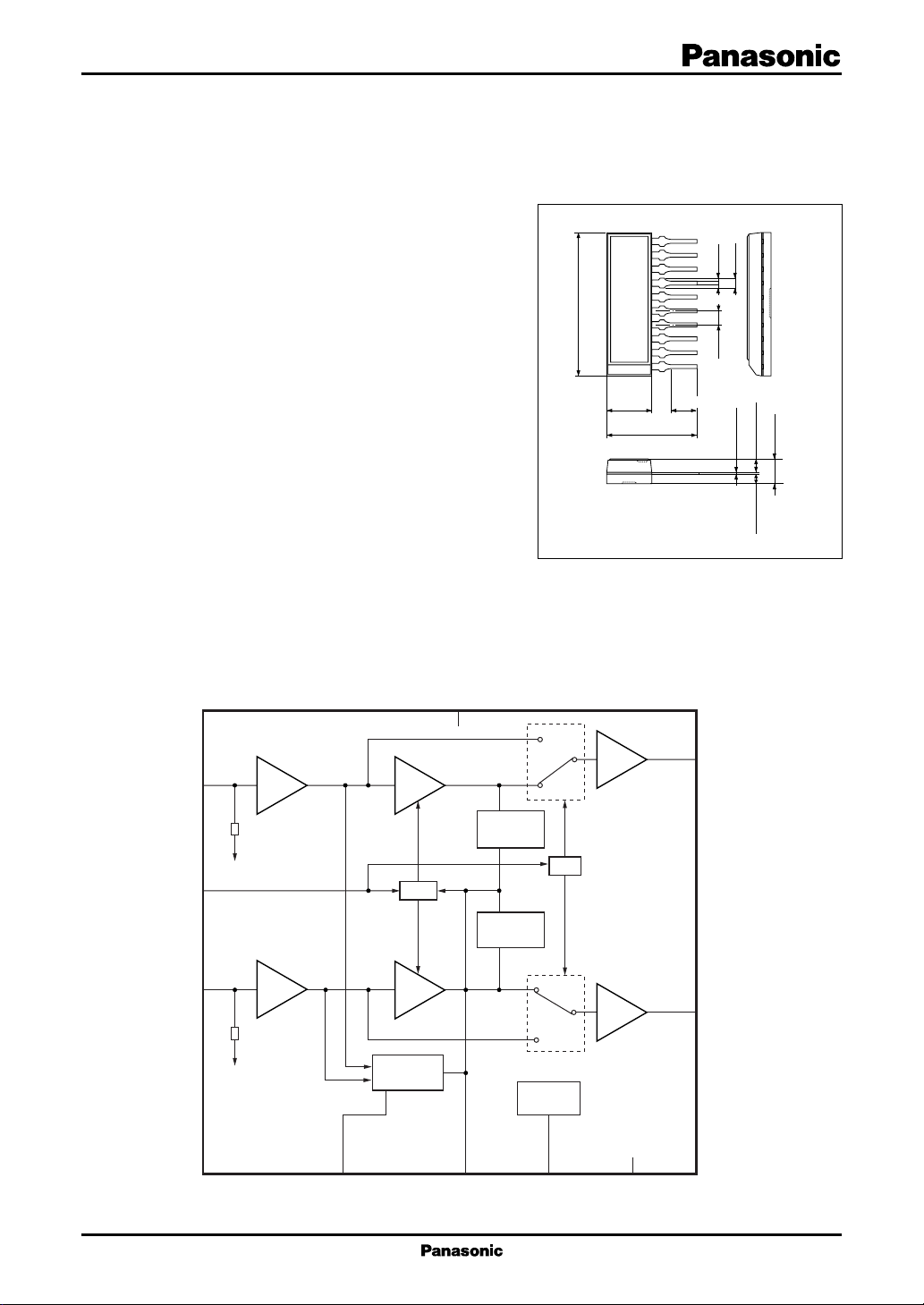
■ Block Diagram
0.5
1.778
+0.1
1.1
–0.05
0.25
Unit: mm
1.65±0.25
3.0±0.3
1.1±0.25
10
18.24±0.3
1
6.0±0.3
CC
V
3.5±0.25
(12.0)
SSIP010-P-0000
4
LIN
CTL
RIN
1
7
10
50 kΩ
50 kΩ
9
LS2
VCA
CTL
VCA
Level
sensor 2
2
LS1
Level
sensor 1
Level
sensor 1
V/l reg.
3
LOUT
SW
8
ROUT
5
REF
V
6
GND
1
Page 2

AN5285K ICs for T V
■ Absolute Maximum Ratings
Parameter Symbol Rating Unit
Supply voltage V
Supply current I
Power dissipation P
Operating ambient temperature
Storage temperature
Note)*: Except for the operating ambient temperature, and storage temperature, all ratings are for Ta = 25°C.
*
*
CC
CC
D
T
opr
T
stg
■ Recommended Operating Range
Parameter Symbol Range Unit
Supply voltage V
CC
■ Electrical Characteristics at VCC = 12 V, fIN = 1 kHz, Ta = 25°C
Parameter Symbol Conditions Min Typ Max Unit
*
= 3.5 V.
ctl
*
*
*
*
*
*
I
Without input signal 5 10 15 mA
CC
V1 VIN = 1 mV[rms] 0.7 1.0 1.4
V2 VIN = 50 mV[rms] 80 110 140
V3 VIN = 200 mV[rms] 150 200 2 5 0
V4 VIN = 1 V[rms] 200 280 3 60
= 2.5 V 50 100 150
ctl
= 4.5 V 230 300 370
ctl
THD VIN = 200 mV[rms] 0.1 0.5 %
VnNo input signal (with IHF-A) 100 µV[rms]
*
*
*
V
Input level at THD = 1% 2.8 V[rms]
max
SWVIN
= 1 V[rms], V
= 1.2 V 890 1 000 1 130
ctl
CB VIN = 200 mV[rms] −1.0 0 1.0 dB
FC VIN = 200 mV[rms] −1.0 0 1.0 dB
Level difference of fIN = 1 kHz/20 kHz
Supply current
Input and output level 1
Input and output level 2
Input and output level 3
Input and output level 4
Input and output level 5 V5 VIN = 100 mV[rms], V
Input and output level 6 V6 VIN = 300 mV[rms], V
Total harmonic distortion
Noise level
Maximum input level
Crosstalk between channels GT VIN = 2 V[rms], AGC off 60 dB
AGC OFF voltage V
Channel balance
Frequency characteristics
Input and output level 7 V7 VIN = 200 mV[rms], AGC off 175 200 225
Note)*:V
13.0 V
30 mA
390 mW
−20 to +75 °C
−55 to +150 °C
8.5 to 12.5 V
mV[rms]
mV[rms]
mV[rms]
mV[rms]
mV[rms]
mV[rms]
mV[rms]
mV[rms]
2
Page 3

ICs for TV AN5285K
■ Terminal Equivalent Circuits
Pin No. Equivalent circuit Description Voltage
1 LIN: 6 V
Left side input pin
1
2 LSI: 0.5 V
200 Ω
50 kΩ
1/2 V
CC
Level 1 Level 2 CTL
AGC level sensor 1 and 2 to
1.5 V
20 kΩ
430 Ω
2
3 LOUT: 6 V
Left side output pin
143 Ω
3
143 Ω
4 VCC :
VCC pin
5V
:6 V
REF
Reference voltage stability
50 kΩ
5
200 Ω
50 kΩ
6 GND:
GND pin
3
Page 4

AN5285K ICs for T V
■ Terminal Equivalent Circuits (continued)
Pin No. Equivalent circuit Description Voltage
7 CTL:
AGC on/off changeover
96 kΩ
20 kΩ
20 kΩ
200 Ω
40 kΩ
8 ROUT: 6 V
143 Ω
8
AGC off at 1.2 V or lower
7
Right side output pin
143 Ω
9 LS2: 6 V
AGC level sensor 2
18 kΩ
900 Ω
250 Ω
1/2 V
CC
9
10 RIN: 6 V
Right side input pin
200 Ω
10
50 kΩ
1/2 V
CC
4
Page 5

ICs for TV AN5285K
■ Application Circuit Example
CC
V
4
4.7 µF
LIN
4.7 µF
3
1
VCA
LOUT
RIN
24 kΩ10 kΩ
4.7 µF
CTL
7
10
50 kΩ
50 kΩ
9
LS2
Level
sensor 2
10 µF
CTL
VCA
Level
sensor 1
SW
Level
sensor 1
4.7 µF
8
V/l Reg.
REF
V
5
6
GND
10 µF
2
LS1
2.2 MΩ
4.7 µF
ROUT
5
 Loading...