

Page 1
AN-501
()(
π
=
(
)
(
π
=
One Technology Way • P.O. Box 9106 • Norwood, MA 02062-9106, U.S.A. • Tel: 781.329.4700 • Fax: 781.461.3113 • www.analog.com
APPLICATION NOTE
Aperture Uncertainty and ADC System Performance
by Brad Brannon and Allen Barlow
APERTURE UNCERTAINTY
Aperture uncertainty is a key ADC concern when performing
IF sampling. The terms aperture jitter and aperture uncertainty
are synonymous and are frequently interchanged in the
literature. Aperture uncertainty is the sample-to-sample
variation in the encoding process. It has three distinct effects on
system performance. First, it can increase system noise. Second,
it can contribute to the uncertainty in the actual phase of the
sampled signal itself giving rise to increases in error vector
magnitude. Third, it can heighten intersymbol interference
(ISI). However, in typical communications applications, an
aperture uncertainty that is sufficiently small to meet system
noise constraints results in negligible impact on phase
uncertainty and ISI. For example, consider the case of sampling
an IF of 250 MHz. At that speed, even 1 ps of aperture jitter can
limit any ADC’s SNR to only 56 dB, while for the same
conditions, the phase uncertainty error is only 0.09 degrees rms
based on a 4 ns period. This is quite acceptable even for a
demanding specification such as GSM. The focus of this
analysis is, therefore, on overall noise contribution due to
aperture uncertainty.
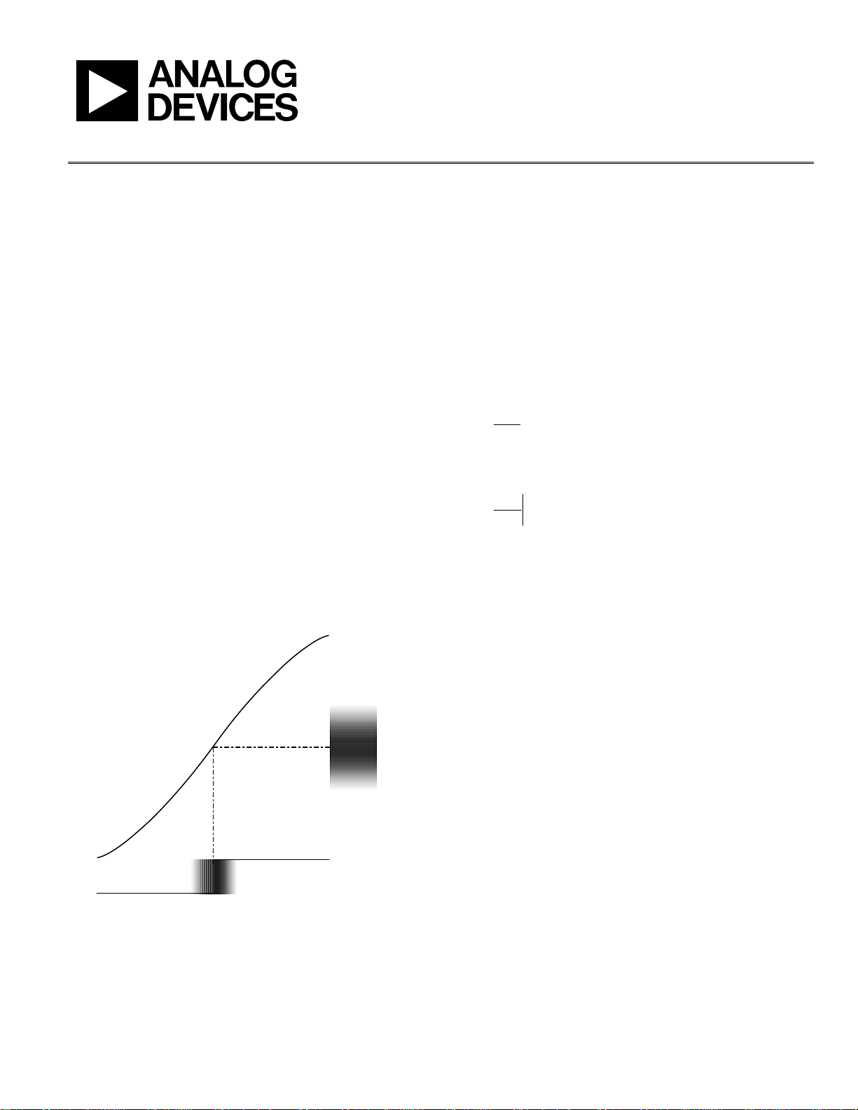
Figure 1 illustrates how an error in the sampling instant results
in an error in the sampled voltage. Mathematically, the
magnitude of the sampled voltage error is defined by the time
derivative of the signal function. Consider a sine wave input
signal
(1)
)
ftAtv
2sin
The derivative is
tdv
dt
The maximum error occurs when the cosine function equals 1,
that is, at t = 0.
)
dv
0
dt
max
We s e e fr o m
corresponding to the jitter dt. For conceptual clarity, if we
relabel dv as V
factors, we get
fA
π
2
=
Figure 1 that dv is the error in the sampled voltage
and dt as ta (aperture error) and rearrange the
err
(4)
ftAV
2
aerr
(2)
(
)
ftfA
ππ
2cos2=
(3)
ENCODE
dt
Figure 1. RMS Jitter vs. RMS Noise
ERROR VOLTAGE
dv
01399-001
Rev. A | Page 1 of 4
If t
is given as an rms value, the derived V
a
Although this is the error at maximum input slew and
represents an upper bound rather than a nominal, this simple
model proves surprisingly accurate and useful for estimating
the degradation in SNR as a function of sample clock jitter.
is also rms.
err
JITTER AND SNR
As Equation 4 indicates, the error in the sampled voltage
increases linearly with input frequency, so at high frequencies,
for example, in IF sampled receiver applications, clock purity
becomes extremely important. Sampling is a mixing operation:
the input signal is multiplied by a local oscillator or in this case,
a sampling clock. Because multiplication in time is convolution
in the frequency domain, the spectrum of the sample clock is
convolved with the spectrum of the input signal. Considering
that aperture uncertainty is wideband noise on the clock, it
shows up as wideband noise in the sampled spectrum, periodic
and repeated around the sample rate.
Page 2
AN-501
W
A
Because ADC encode inputs have very high bandwidth, the
effects of clock input noise can extend out many times the
sample rate itself and alias back into the baseband of the
converter. Therefore, this wideband noise degrades the noise
floor performance of the ADC. Consider a sinusoidal input
signal of amplitude A. Utilizing Equation 4, the SNR for an
ADC limited by aperture uncertainty is
SNR
A
V
err
(5)
(
ft
π
2log20log20 −==
)
a
Equation 5 illustrates why systems that require high dynamic
range and high analog input frequencies also require a low jitter
encode source. For an analog input of 200 MHz and only
300 femtoseconds rms clock jitter, SNR is limited to only
68.5 dB, well below the level commonly achieved at lower
speeds by 12-bit converters. Note in Equation 5 that the jitter
limit of SNR is independent of the converter resolution. (For
the case just mentioned, a 14-bit converter would do no better.)
Aperture jitter is not always the performance limiter. Equation 6
shows its effect in superposition with other noise sources. The
first term in the brackets is the jitter from Equation 5. To that,
we must add terms for quantization noise, DNL, and thermal
noise. For other analytic purposes, each of these could be
broken out separately, but for simplicity in isolating the effect of
jitter, we combine them here in a single additional term.
2/1
2
⎡
2
()
tfSNR
2log20
π
⎢
⎢
⎣
+−=
a
⎤
1
ε
+
⎛
⎜
2
⎝
(6)
⎞
⎟
⎥
N
⎠
⎥
⎦
where:
f = analog input frequency.
t
= aperture uncertainty (jitter).
a
ε = “composite rms DNL” in LSBs, including thermal noise.
N = number of bits.
This simple equation provides considerable insight into the
noise performance of a data converter.
MEASURING SUBPICOSECOND JITTER
Aperture uncertainty is readily determined by examining SNR
without harmonics as a function of analog input frequency. Two
measurements are required for the calculation. The first
measurement is done at a sufficiently low analog input
frequency that the effects of aperture uncertainty are negligible.
Since jitter is negligible, Equation 6 can be simplified and
rearranged to solve for ε, the “composite DNL.”
−SNR
N
20
1102
−×=ε
(7)
Next, an FFT is done at high (IF) frequency. The high frequency
chosen should be as high as possible. Again, the SNR value
without harmonics is measured. This time jitter is a contributor
to noise and solving Equation 6 for t
2
SNR
−
10
⎞
20
⎟
⎟
⎠
π
2
ε
1
+
⎛
−
⎜
N
2
⎝
f
⎛
⎜
⎜
⎝
t
=
a
yields
a
2
⎞
⎟
⎠
(8)
where:
SNR = the high frequency SNR just measured
ε = the value determined in the low frequency measurement.
EXAMPLE: JITTER AND THE AD9246
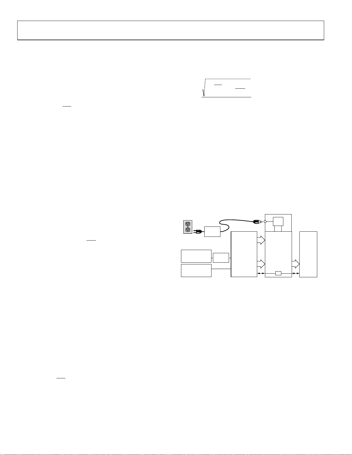
The example shown here utilizes the AD9246 evaluation board,
a 14-bit, 125 MSPS ADC. An external clock oscillator such as a
Wenzel Sprinter or Ultra-Low Noise provides a suitable encode
source. A mainstream RF synthesizer from Rohde & Schwarz or
Agilent can be used for the analog source. Typically, these
generators have insufficient phase noise performance for use as
the encode source. For more information about configuring
Analog Devices evaluation boards, please consult the individual
product data sheet.
LL OUTLET
100V TO 240V AC
47Hz TO 63Hz
6V DC
PARALLEL
BOARD
PARALLEL
CHB
CMOS
OUTPUTS
CHA
CMOS
OUTPUTS
2A MAX
ROHDE & SCHWARZ,
SMHU,
2V p-p SIGNAL
SYNTHESIZER
ROHDE & SCHWARZ,
SMHU,
2V p-p SIGNAL
SYNTHESIZER
SWITCHING
POWER
SUPPLY
BAND-PASS
FILTER
EVALUATION
XFMR
INPUT
CLK
Figure 2. Aperture Uncertainty Measurement Setup with AD9246 Customer
Evaluation Board
Figure 3 is a 5 average, 64 K FFT of the AD9246 sampling a 2.3
MHz sine wave at 125 MSPS. Analog Devices’ ADC Analyzer
Software (
www.analog.com/fifo) collects and processes the data
to report SNR without harmonics. From the plots, the SNR is
72.05 dBFS.
3.3V
–+
VCC
GND
HSC-ADC-EVALB-DC
FIFO DATA
CAPTURE
BOARD
USB
CONNECTION
SPI
PC
RUNNING
ADC
ANALYZER
SPISPI
TM
01399-002
Here, SNR is the low frequency value just measured.
Rev. A | Page 2 of 4
Page 3

AN-501
Device: AD9246
Device No.: 1
Avcc: 1.8 Volts
Dvcc: 1.8 Volts
Encode: 125. MSPS
Analog: 2.3 MHz
SNR: 71.06 dB
SNRFS: 72.05 dBFS
UDSNR: 96.62 dB
NF: 30.69 dB
SINAD: 70.87 dB
Fund: –0.999 dBfs
2nd: –90.62 dBc
3rd: –86.59 dBc
4th: –104.15 dBc
5th: –108.51 dBc
6th: –94.04 dBc
WoSpur: –90.53 dBc +
THD: –84.55 dBc
SFDR: 86.59 dBc
Noise Floor: –117.21 dBFS
Samples: 65536
Windowing: None
Using this value for SNR in Equation 7 gives a “composite DNL
(ε)” for this converter of 3.09 LSB.
Next, the degradation in SNR as a function of analog input
frequency is found.
clock, but using an analog input frequency of 201 MHz. Here, the
noise floor has risen and the resulting SNR is 69.05 dBFS.
Device: AD9246
Device No.: 1
Avcc: 1.8 Volts
Dvcc: 1.8 Volts
Encode: 125. MSPS
Analog: 49.004 MHz
SNR: 67.98 dB
SNRFS: 69.05 dBFS
UDSNR: 93.4 dB
NF: 33.69 dB
SINAD: 66.75 dB
Fund: –1.069 dBfs
2nd: –78.21 dBc
3rd: –74.41 dBc
4th: –103.12 dBc
5th: –104.29 dBc
6th: –93.26 dBc
WoSpur: –90.65 dBc +
THD: –72.85 dBc
SFDR: 74.41 dBc
Noise Floor: –114.2 dBFS
Samples: 65536
Windowing: None
Using this SNR and the previous solution for ε, Equation 8 gives
t
a
This value, 197 fs, is the combined aperture uncertainty for the
AD9246 plus the clock oscillator. Since total noise squared is the
sum of the squares of individual contributors, the jitter of the
ADC itself is readily determined if the jitter of the source clock
is known. Here a Wenzel ULN clock oscillator with about 50 fs
jitter is used, giving a jitter for the ADC of about 190
simple measurements confirm that it is possible to measure very
small aperture uncertainty numbers using readily available
hardware and simple numeric calculations.
0
–10
–20
–30
–40
–50
–60
–70
–80
3
2
–90
–100
–110
–120
–130
010
6
4
5
5 1520253035404550 5560
+
FREQUENC Y (MHz)
Figure 3. 2.3 MHz FFT
Figure 4 shows data from the same setup and
01399-003
Figure 5 overlays plots of Equation 5 for various jitter values
(the sloped lines) with ideal, quantization noise limited
performance at various resolutions (the horizontal lines), and is
a useful guide for quickly determining jitter limits based on
analog input frequency and SNR requirements.
100
90
0
0
.
.2
80
2
p
s
SNR (dB)
70
60
50
10 100 1000
0
.5
1
p
p
s
s
INPUT (MHz)
1
2
5
5
p
p
s
s
Figure 5. Signal-to-Noise Ratio Due to Aperture Jitter
16 BITS
14 BITS
12 BITS
10 BITS
01399-005
CLOCK DISTRIBUTION
System clocks commonly must be distributed to multiple
0
–10
–20
–30
–40
–50
–60
–70
–80
–90
–100
5
–110
–120
–130
5 1520 2530354045505560
010
3
2
+
FREQUENC Y (MHz)
6
4
01399-004
Figure 4. 201 MHz FFT
2
−
05.69
⎛
⎜
10
⎜
⎝
=
⎞
+
20
⎛
⎟
−
⎜
⎟
⎝
⎠
π
102012
×
2
092.31
⎞
⎟
14
2
⎠
6
=
(9)
rmsfs197
. These
fs
converters, and additionally to the FPGAs, ASICs, and DSPs
included in the signal chain. There are several ways to distribute
clocks with the low jitter demanded by the converters.
If the sample clock is generated as a sinewave, it can be
distributed using power dividers and delivered to the ADC with
a transformer as shown in
Figure 6. This solution is simple and
works well for many applications, especially in situations
involving single-ended to differential conversion.
However, more often than not the clock is a logic signal sourced
directly from a PLL, VCO, or VCXO. In these cases, it is
advantageous to use logic gates to fan out the signal and to drive the
data converters.
Table 1 summarizes the typical jitter that can be
achieved with a variety of logic families. It should be noted that
many of the older families, and even current FPGAs, cannot deliver
acceptable performance. Some newer, high-speed devices do
provide acceptable jitter and have the ability to translate singleended signals into differential signals as shown in
Figure 7.
Table 1.
Gate Type Jitter
1
FPGA
33 to 50 ps
74LS00 4.94 ps
74HCT00 2.20 ps
74ACT00 0.99 ps
MC100EL16 (PECL) 0.70 ps
AD9510 Clock Synthesis and Distribution 0.22 ps
NBSG16 (Reduced Swing ECL) 0.20 ps
1
Does not include the jitter introduced by input structure or internal routing
gates, or the jitter associated with the use of internal DLL/PLL structures.
Based on product data sheet peak-to-peak values ranging from ±100 ps to
±300 ps peak.
Rev. A | Page 3 of 4
Page 4

AN-501
S
VSV
V
CLOCK
OURCE
0.1µF
ADT1–1WT
HSMS2812
DIODES
CLK+
AD9444
CLK–
1399-006
Figure 6. Distribution and Differential Encode Options
T
0.1µF
ECL/
PECL
VT
0.1µF
ENCODE
AD9444
ENCODE
01399-007
Figure 7. Active Differential Drive Circuit
Clock trees employing cascaded gates are commonly used in
digital circuits (see
Figure 8), but jitter accumulates as the clock
progresses down the tree.
ADC ENCODE INPUT
SYSTEM CLOCK
(A)
SYSTEM CLOCK
(B)
Figure 8. Clock Distribution Chains
ADC DATA LATCH
DAC CLOCK INPUT
DACDATALATCH
ADC ENCODE INPUT
In addition, the AD9510 includes many other features not
available in discrete logic such as selectable output types (LVDS,
PECL, and CMOS) and programmable fine delays.
Figure 10
shows how the AD9510 can be used in a typical low jitter
solution.
RSET
GND
DISTRIBUTION
REFIN
REFINB
SYNCB,
FUNCTION
CLK1
CLK1B
SCLK
SDIO
SDO
CSB
01399-008
RESETB
PDB
SERIAL
CONTROL
PORT
REF
R DIVIDER
N DIVIDER
PROGRAMM ABLE
AD9510
FREQUENCY
DETECTOR
DIVIDERS AND
PHASE ADJUST
/1, /2, /3... /31, /32
/1, /2, /3... /31, /32
/1, /2, /3... /31, /32
/1, /2, /3... /31, /32
/1, /2, /3... /31, /32
/1, /2, /3... /31, /32
/1, /2, /3... /31, /32
/1, /2, /3... /31, /32
PHASE
Figure 9. AD9510 Clock Synthesis and Distribution
CPRSET
CP
PLL
REF
CHARGE
PUMP
PLL
SETTINGS
LVPECL
LVPECL
LVPECL
LVPECL
LVDS /C MOS
LVDS /C MOS
ΔT
LVDS /C MOS
ΔT
LVDS /C MOS
CP
STATUS
CLK2
CLK2B
OUT0
OUT0B
OUT1
OUT1B
OUT2
OUT2B
OUT3
OUT3B
OUT4
OUT4B
OUT5
OUT5B
OUT6
OUT6B
OUT7
OUT7B
01399-009
In a cascade of just three NBSG16 gates (one of the better
performers), the cumulative rms jitter increases to 350 fs, which
is a significant impact on system performance of an IF sampling
system. It is better to avoid conventional clock trees altogether,
and instead, approach clock generation and distribution as a
system level function.
Devices such as the AD9510 have optimized the clock paths to
minimize total rms noise. By comparing
Figure 8 and Figure 9,
it is clear that the AD9510 offers the same function for clock
distribution as that in
Figure 8, but with an additive jitter of
only 220 fs. In addition, this part includes an ultra low noise
PLL similar to the ADF4106 that allows complete clock cleanup,
synthesis, and distribution in a single package.
©2006 Analog Devices, Inc. All rights reserved. Trademarks and
registered trademarks are the property of their respective owners.
AN01399-0-3/06(A)
Rev. A | Page 4 of 4
DSP
16
IF = ~190MHz
491.52MHz
LOOP FILTER
VCXO
IF = ~190MHz
IF = ~190MHz
32.768MHz
REFERENCE
92.16MHz
92.16MHz
92.16MHz
AD9510
92.16MHz
14
92.16MHz
14
Figure 10. Typical Clock Distribution Application
TXAD9786AD6633
MAIN TX
RXAD9246AD6636
MAIN RX
RXAD9246AD6636
DIVERSITY
RX
01399-010
 Loading...