

Page 1
ICs for VCR
AN3895FHQ
Cylinder/capstan motor driver IC for video camera
■ Overview
The AN3895FHQ is an IC designed for driving a
cylinder/capstan motor for a video camera.
■ Features
• Operating supply voltage range: VCC = 3.1 V to 5.5 V
Cylinder block
• Reduction of magnetic sound due to 3-phase full wave
overlap driving
• Built-in standby mode for power saving
• Built-in PG·FG and waveform shaping circuit
• Built-in switching power supply control circuit
Capstan block
• Overlap driving
• Built-in torque ripple cancel circuit
• Built-in switching power supply control circuit
• Built-in output transistor saturation prevention circuit
for both lower and upper sides
• Forward/reverse rotations
■ Applications
• Video camera
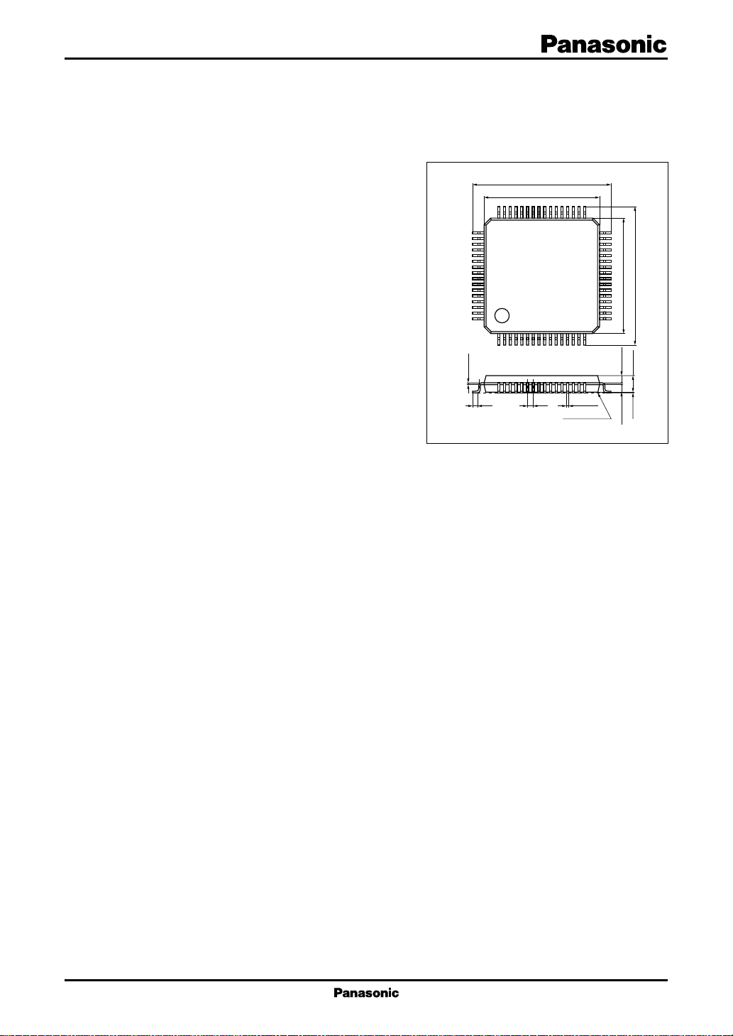
12.0±0.4
10.0±0.3
48 33
49
64
116
+0.10
–0.05
0.15
(0.5)(0.5)
+0.10
0.18
–0.05
Seating plane
LQFP064-P-1010
Unit: mm
32
10.0±0.3
12.0±0.4
17
1.4±0.20.1±0.1
0.625±0.10.625±0.1
1
Page 2
AN3895FHQ ICs for VCR
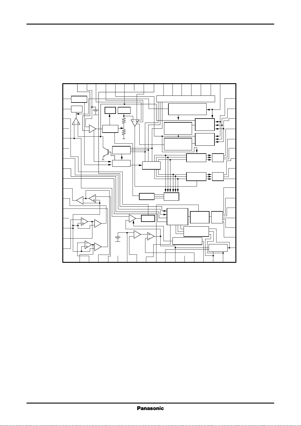
■ Block Diagram
CEC
CECR
CTL
CPCI
CPCV
CPCS
GNDC
CCS
YTEST
CH1+CH1−CH2+CH2−CH3+CH3−VMC
48
47
46
45
44
43
42
41
40
39
38
37
36
35
34
33
49
CRSF
CSWB
YSWB
GSWB
CYFC
V
CC
YCLK
YSL3
YSL2
CFG
YPG
YFG
GPF
PFREF
YPGO
YPCI
R/S/F
50
Amp.
1/N
Mod.
Hall amp. matrix
VM bottom limit short-
circuit protection circuit
51
Upper V
52
Absolute
value
53
54
Direction
det.
55
56
Logic
Direction
switch
57
Upper side
saturation
prevention circuit
Lower side
saturation
prevention circuit
Upper side
distribution
Lower side
distribution
det. circuit
Lower V
det. circuit
CE
CE
Amp.
Amp.
58
Comp.
59
Min.
60
61
Comp.
Amp.
62
63
64
Comp.
Absolute
value
Current flow
phase
changeover
logic
Distribution
BEMF det.
comp.
Va lower limit
Amp.
V
CE
det.
CM1
32
CM2
31
CM3
30
CU3
29
CU2
28
CU1
27
CL1
26
CL2
25
CL3
24
YU3
23
YU2
22
YU1
21
YL1
20
YL2
19
YL3
18
YM1
17
1
2
3
4
5
6
7
8
9
10
11
12
13
14
15
16
YFGO
YFGI
CFGO
CFGI
YSTB
YECR
YEC
YSL1
YPCI
YPCV
YPCS
GNDY
YCS
VMY
YM3
YM2
2
Page 3

ICs for VCR AN3895FHQ
■ Pin Descriptions
Pin No. Description
1 YFGO: CYL-FG amp. output
2 YFGI: CYL-FG amp. input
3 CFGO: CAP-FG amp. output
4 CFGI: CAP-FG amp. input
5 YSTB: CYL-standby input changeover
6 YECR: CYL-torque command reference
input pin
7 YEC: CYL-torque command input pin
8 YSL1: CYL-current flow waveform slope pin 1
Pin No. Description
34 CH3− : CAP-Hall element input
35 CH3+ : CAP-Hall element input
36 CH2− : CAP-Hall element input
37 CH2+ : CAP-Hall element input
38 CH1− : CAP-Hall element input
39 CH1+ : CAP-Hall element input
40 YTEST: CYL-test mode changeover input
41 CCS: CAP-current det. pin
42 GNDC: CAP-grounding pin
9 YPCI: CYL-current feedback phase
compensation
10 YPCV: CYL-voltage feedback phase
compensation
11 YPCS: CYL-switching power supply
control output
12 GNDY: CYL-grounding pin
13 YCS: CYL-CS current det. pin
14 VMY: CYL-motor power supply pin
15 YM3: CYL-motor coil pin 3
16 YM2: CYL-motor coil pin 2
17 YM1: CYL-motor coil pin 1
18 YL3: CYL-lower side pre-drive output 3
19 YL2: CYL-lower side pre-drive output 2
20 YL1: CYL-lower side pre-drive output 1
21 YU1: CYL-upper side pre-drive output 1
22 YU2: CYL-upper side pre-drive output 2
23 YU3: CYL-upper side pre-drive output 3
24 CL3: CAP-lower side pre-drive output 3
25 CL2: CAP-lower side pre-drive output 2
26 CL1: CAP-lower side pre-drive output 1
27 CU1: CAP-upper side pre-drive output 1
28 CU2: CAP-upper side pre-drive output 2
29 CU3: CAP-upper side pre-drive output 3
30 CM3: CAP-motor coil pin 3
31 CM2: CAP-motor coil pin 2
32 CM1: CAP-motor coil pin 1
33 VMC: CAP-motor power supply pin
43 CPCS: CAP-switching power supply control
output
44 CPCV: CAP-voltage feedback phase
compensation
45 CPCI: CAP-current feedback phase
compensation
46 CTL: CAP-torque limit
47
48 CEC: CAP-torque command input pin
49 CRSF: CAP-direction command input pin
50 CSWB: CAP-SW-power supply pre-drive
51 YSWB: CYL-SW-power supply pre-drive
52
53
54 VCC -power supply pin
55 YCLK: CYL-clock input
56
57
58
59
60
61 GPF: FG, PG-grounding pin
62 PFREF: FG, PG-reference voltage
63 YPGO: CYL-PG amp. output
64 YPCI: CYL-PG amp. input
CECR: CAP-torque command reference voltage
output
output
GSWB: CAP, CYL-SW power supply grounding pin
CYFC: CAP, CYL-SW comparater triangular
wave input
YSL3: CYL-current flow waveform slope pin 3
YSL2: CYL- current flow waveform slope pin 2
CFG: CAP-FG amp. waveform shaping output
YPG: CYL-PG amp. waveform shaping output
YFG: CYL-FG amp. waveform shaping output
3
Page 4

AN3895FHQ ICs for VCR
■ Absolute Maximum Ratings
Parameter Symbol Rating Unit
Supply voltage V
Supply current I
Power dissipation P
1
Operating ambient temperature
1
Storage temperature
Motor supply voltage
Output pin voltage
*
2
*
3
*
*
Switching power supply driving V
output pin voltage
Pin voltage
Note)
1: Except for the operating ambient temperature and storage temperature, all ratings are for Ta = 25°C.
1. *
2: m = 14, 33
*
3: n = 15 to 32
*
4: l = 50, 51
*
3: o = 2, 4, 5, 7, 8, 13, 34 to 41, 46 to 49, 53, 55 to 57, 59, 62, 64
*
2. Do not apply external currents or voltages to any pins not specifically mentioned.
3. For circuit currents, '+' denotes currents flowing into the IC, and '−' denotes current flowing out of the IC.
*4
5
*
CC
CC
D
T
opr
T
stg
V
m
V
n
l
V
o
6.0 V
mA
582 mW
−20 to +70 °C
−55 to +125 °C
12.0 V
12.0 V
12.0 V
− 0.3 to VCC +0.3 V
■ Recommended Operating Range
Parameter Symbol Range Unit
Supply voltage V
CC
3.1 to 5.5 V
■ Electrical Characteristics at Ta = 25°C
Parameter Symbol Conditions Min Typ Max Unit
Cylinder block
Supply current 1 I
Supply current 2 I
Torque command reference voltage
V
Torque command input current I
Torque command input offset ∆YEC −100 −40 100 mV
voltage
Input/output gain YG
Output maximum voltage YCS
Lower side output voltage 1 YVL(1) YVCS = 54 mV 0.20 0.40 0.60 V
Lower side output voltage 2 YVL(2) YECR = 2.24 V, YEC = 0 V 0.50 0.71 0.90 V
Upper side driving current 1 YI
Lower side output current 2 YI
Common for both cylinder and capstan 22 30 mA
CC(1)
in operation
At STB mode of cylinder 12 20 mA
CC(2)
YECR
YEC
io
maxYRCS
U
L
= 0.27 Ω 150 180 210 mV
2.14 2.24 2.54 V
−5 − 0.7 µA
0.13 0.15 0.17 times
10 30 mA
−23 −10 mA
4
Page 5

ICs for VCR AN3895FHQ
■ Electrical Characteristics at Ta = 25°C (continued)
Parameter Symbol Conditions Min Typ Max Unit
Cylinder block (continued)
SW power supply control output V
voltage 1 V
SW power supply control output V
voltage 2 V
SW power supply control output G
gain
SW reg. driving current 1 I
SW reg. driving current 2 I
YSW(1)
YSW(2)
SW reg. comparator on time Yt
SW reg. comparator off time Yt
SW reg. comparator offset voltage ∆V
FG amp. gain YGFGV[p-p] = 1.5 mV, f = 1 kHz 45 48 dB
YFG high-level YFG(H) IYFG = −100 µA 2.0 2.6 V
YFG low-level YFG(L) IYFG = 100 µA 0.7 1.5 V
PG amp. gain YGPGV[p-p] = 1.5 mV, f = 1 kHz 45 48 dB
PG amp. offset voltage ∆YPG
YPG high-level YPG(H) IYPG = −10 µA 2.0 2.9 V
YPG low-level YPG(L) IYPG = 100 µA 0.3 1.0 V
Standby voltage
Standby reset voltage
YSTB
YSTB
Standby input current I
Capstan block
Torque command input current I
Torque command reference voltage
V
Torque command input voltage V
Output maximum voltage CCS
Torque command I/O gain CG
Output idle voltage CCS
Torque command input offset CEC
voltage
Torque command dead zone CEC
Lower side VCE voltage 1 CV
Lower side VCE voltage 2 CV
Hall element input allowable CH
voltage
Offset referred to Hall element CH
input
YEC = 2.14 V, YECR = 2.24 V, 0.26 0.37 0.48 V
YUD(1)
= 1.75 V
YPCS
YEC = 0 V, YECR = 2.24 V, 0.43 0.61 0.81 V
YUD(2)
= 1.75 V
YPCS
YEC = 2.14 V, YECR = 2.24 V 6.5 9 11 times
YPCS
YEC = YECR = 2.24 V 3 9 mA
YEC = 0 V, YECR = 2.24 V 11 23 mA
ON
OFF
YFC
IN
ON
OFF
YSTBVYSTB
CEC
CECR
CEC
maxRCS
IO
IDLE
OFC
DZ
LL(1)
LL(2)
IN
OFS
= 0 V −100 µA
CEC = CECR = 1.75 V −1 0.2 µA
= 0.3 Ω 0.19 0.22 V
CCS = 60 mV 0.19 0.29 0.47 V
CEC = 0 V, CTL = 0.2 V 0.40 0.61 0.77 V
0.2 1.0 µs
0.2 1.0 µs
−5425mV
0.45 0.52 0.62 V
2.15 1.4 V
1.4 0.6 V
1.55 1.75 1.95 V
0.5 3.0 V
0.21 0.24 0.27 times
04mV
−100 −40 100 mV
50 90 140 mV
1.2 2.4 V
−80 8mV
5
Page 6

AN3895FHQ ICs for VCR
■ Electrical Characteristics at Ta = 25°C (continued)
Parameter Symbol Conditions Min Typ Max Unit
Capstan bock (continued)
TL-CS offset 1
Forward rotation command voltage V
Stop command voltage V
Reverse rotation command voltage V
Ripple rejection factor α CS = 60 mV 8 13 18 %
Upper side driving max. current CI
Lower side driving max. current CI
SW power supply input offset SW
SW power supply output gain G
SW power supply output voltage 1 V
SW power supply output voltage 2 V
SW reg. driving current 2 I
SW power supply comparator t
on time
SW power supply comparator t
off time
FG-PG amp. reference voltage PFREF 1.7 2.0 2.3 V
FG amp. loop gain CG
FG amp. high-level output voltage CFGH I
FG amp. low-level output voltage CFGL I
VM under limit CV
VM short-circuit protection CV
CTL
SWB(2)
OFS(1)
F
S
R
U
L
OFS
CPCS
CEC = CECR, CPCS = 1.7 V 0.20 0.29 0.40 V
UD(1)
CEC = 0 V, CTL = 0.2 V, 0.47 0.72 1.10 V
UD(2)
61014mV
1.0 0.87 V
1.27 2.23 V
2.63 2.45 V
10 40 mA
−20 −10 mA
−25 0 15 mV
8.0 10.6 13.0 times
CPCS = 1.7 V
CEC = 0 V, CTL = 0.2 V 15 22 mA
ON
OFF
External 1 kΩ, 300 kΩ,4548 dB
FG
0.2 1 µs
0.2 1 µs
input 3 mV[p-p], 1 kHz
= −100 µA 2.0 2.6 V
CFG
= 100 µA 0.8 1.5 V
CFG
ML
MS
1.13 1.45 1.88 V
0.26 0.44 1.00 V
• Design reference data
Note) The characteristics listed below are theoretical values based on the IC design and are not guaranteed.
Parameter Symbol Conditions Min Typ Max Unit
Slope pin charge current I
Slope pin discharge current I
YSCH
YSDCH
−25 µA
25 µA
6
 Loading...