

Page 1
■ Overview
The AN3389SB is a multi-functional recording and playback IC with built-in auto-tracking interface, and automatic head selector at special playback for 4-head VCR.
■ Features
•
Single power supply : VCC=5V typ.
•
Built-in AGC circuit for recording current control
•
Automatic head switching for special playback
•
Built-in an automatic tracking interface
1
ICs for VCR
AN3389SB
Recording/Playback Amplifier IC for 4-Head VCR
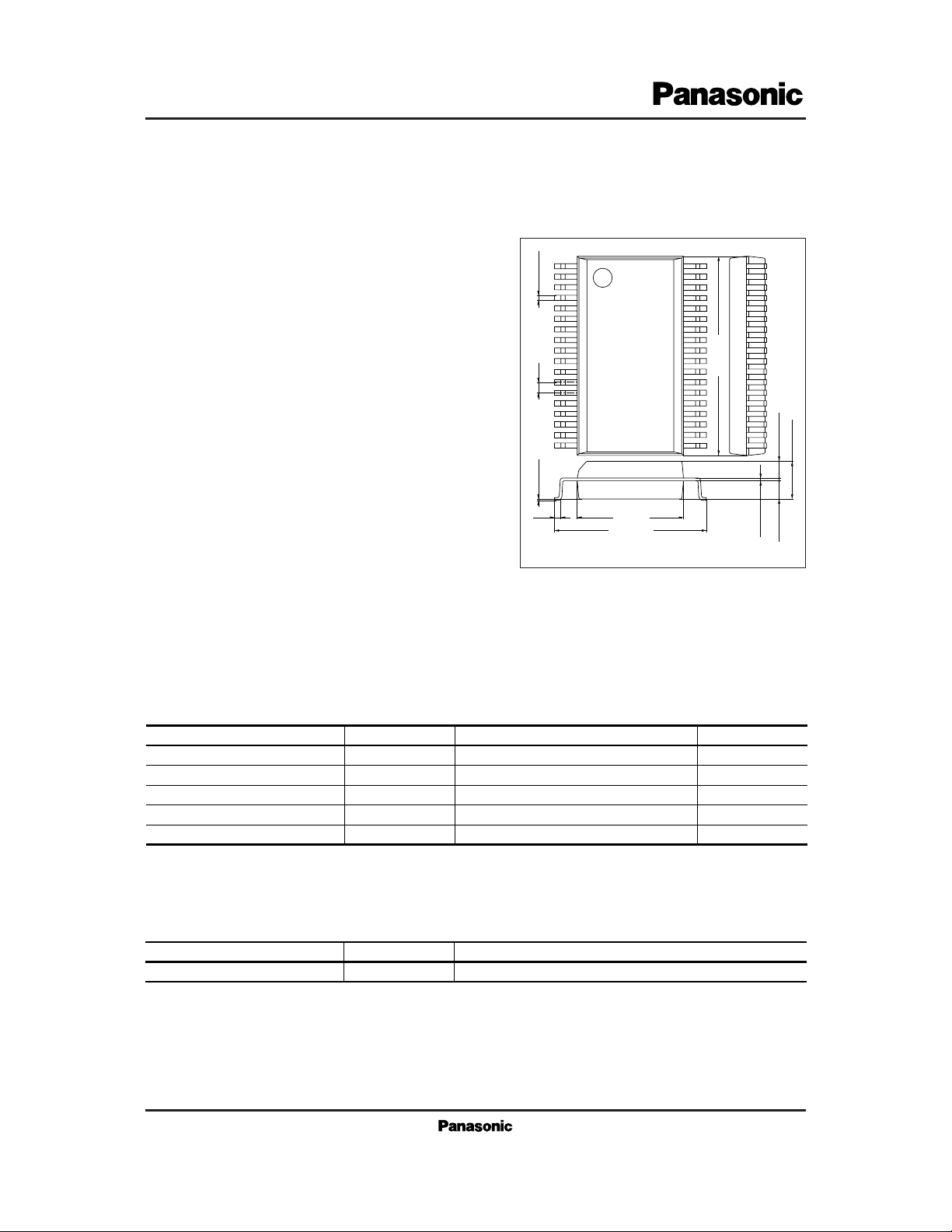
Unit : mm
0.35±0.1
15.2±0.3
0.80.1±0.1
0.5
2.85±0.2
1.3±0.251.3±0.25
0.2
+ 0.1
– 0.05
11.93±0.3
8.4±0.3
36-Pin SSOP Package (SSOP036-P-0450A)
■ Absolute Maximum Ratings (Ta=25 ˚C)
Parameter Symbol Rating Unit
Supply voltage
Supply voltage
Power dissipation
Note 2)
Note 2)
Note 3)
Operating ambient temperature
Storage temperature
Note 1)
Note 1)
V
CC
I
CC
P
D
T
opr
T
stg
5.6 V
160
930
–20 to + 70
–55 to + 125
mA
mW
˚C
˚C
Note 1) Ta=25˚C except operating ambient temperature and storage temperature.
Note 2) Guaranteed values if RADJ is 20kΩ or more.
If RADJ is less than 20kΩ, ensure that the stated power dissipation is not exceeded.
Note 3) The power dissipation is that of a package at Ta=70˚C as mounted on the standard PC board.
■ Recommended Operating Range (Ta=25˚C)
Operating supply voltage range
Parameter Symbol Range
V
CC
4.5V to 5.5V
Page 2
2
ICs for VCR
AN3389SB
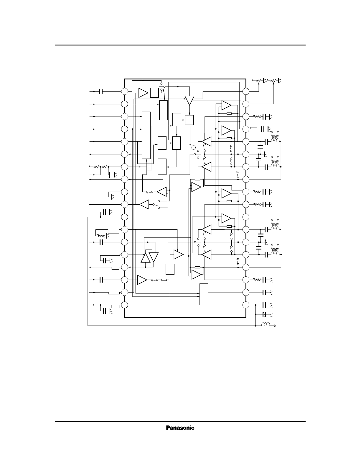
36 35 34 33 32 31 30 29 28 27 26 25 24 23 22 21 20 19
123456789101112131415161718
V
CC
47kΩ
47kΩ
V
CC
VGCTLAGCTLDUMP2
1kΩ
0.01µF
0.1
µF
HOLD
MINDCFB
68pF
68pF
CH2GND2CH1
0.1µF
HEADHEAD
SPCOMDUMP1DUMP2
1kΩ1kΩ
0.01
µF
0.01
µF
REFCH4
0.1µF
68pF
68pF
GND1CH3
0.1µF
HEADHEAD
0.1µF
EPCOMDUMP3CHARGE
RECAGC
DET
V
CC1
1kΩ
0.01
µF
0.1
µF
0.01
µF
33
µF
100µF
V
CC
(typ.5V)
SW1SW2
SW5
SP
(–)
SW4SW3
SW6
SW8SW7
HASW1
CH3
CH4
SW9 SW10
HASW2
CH3 CH4
Rec Det.
Amp.
V–I
1kΩ
MUTE
SW
EF
Det.
AGC
Amp.
HASW
EP SP
ENV
ENV
COMP
SW
AT OUT TIM
S/H V–I
Det.
CHARGE
2
LOGIC (EvSWControl)
MUTE SW
Amp.
HPF
VCA
0.01µF
0.002
µF
0.1µF
0.002
µF
RADJ 47kΩ
SLOW SW
RECEQ
VASEL
(VIDEO : H,
AUDIO : L)
RECIN
AGC OUT
PBRECSW
AGC DET
PLUSCFB
AGC
IN
ICCADJ
RECAGC-
ADJ
0.01
µF
V
CC2
PB OUT GND3 ATOUT
390pF
V
CC
10kΩ
390kΩ
EPSPSW
(EP : H,
SP : L) DEF OUT DEF IN SYNC
PB
CONT
MUTE
SW
AUDIO
IN
0.022
µF
SP
(–)
SP
(+)
EP
(–)
EP
(–)
EP
(+)
+
–
■ Block Diagram
Page 3
3
ICs for VCR
AN3389SB
60 85 110
PB
I
PCQ
At PB
PB quiescent current
Parameter minCondition typ max UnitSymbol
Rec quiescent current
SLOW SW input "L" (Pin36)
Rec/PB input "L" (Pin33)
MUTE SW input "L" (Pin20)
EP/SP input "H" (Pin25)
EP/SP input "L" (Pin25)
DRUM FF input "H" (Pin23)
DRUM FF input "L" (Pin23)
SYNC input "H" (Pin22)
SYNC input "L" (Pin22)
PB CONT input "H" (Pin21)
PB CONT input "M" (Pin21)
PB CONT input "L" (Pin21)
DRUM FF output "H" (Pin24)
DRUM FF output "L" (Pin24)
PB voltage gain
Between CHs gain difference
PB output 2nd harmonics distortion
Input-conversion noise
I
RCQ
V
SL
V
RP
V
MS
V
DFL
V
SYH
V
SYL
V
PCH
V
DOH
GV
∆GV
HDP2
NV
90 120 150
PB
0 1.8
0 1.3
0 1.4
2.9 5.0
0 2.1
1.7 5.0
0 1.0
1.5 5.0
0 0.7
3.8 5.0
1.9 3.1
0 1.1
4.0 5.0
0 1.0
57.5 60.0 62.5
–1.0 0 1.0
V
ESH
V
ESL
V
DFH
V
PCM
V
PCL
V
DOL
At Rec
Input level at SLOW
Input level at Rec
Input level at MUTE OFF
Note
mA
mA
V
V
V
V
V
V
V
V
V
V
V
V
V
V
dB
dB
■ Electrical Characteristics (Ta=25±2˚C)
dB
PB
– 45 – 40 PB
1.0
µVrms
Head change-over DC unbalance
SP selection in AUTO
EP selection in AUTO
–100 0 100
0 1.0
4.0 5.0
V
SP
V
EP
∆V
23
PB
PB
PB
f= 4MHz, 0.5mV
P–P
, CH1 to CH4
I
OUT
= –2mA
IIN= 2mA
f= 4MHz, 0.5mV
P–P
, CH1 to CH4
f= 4MHZ, 0.5mV
P–P
, 8MHz/4MHz
Rg= 10Ω, 1MHzBPF, output/GV
Rg= 10Ω, output DC difference
CH1, CH4 input,Pin24 DC measurement
CH2, CH3 input,Pin24 DC measurement
mV
V
V
V
CA1
V
CA2
AGC level
AGC control characteristics
AGC output 2nd harmonics distortion
Rec amp. gain
Rec AGC level
Rec AGC control characteristics
Recording current 2nd harmonics
distortion
Muting ratio
IOR
I
AGC
HDR2
MR
R
C
∆V
CC
255 320 390
02
–50 – 40
260 360 465
17.8 20.0 22.4
0 1.2
– 40 –35
– 45 – 40
V
AGC
∆V
AGC
HDA2
PB
PB
Rec
Rec
Rec
Rec
Rec
PB
PB
Common terminal ON resistance
Input terminal ON resistance
Output DC drift
VCA output voltage 1
(amp. gain)
VCA output voltage 2
(amp. f characteristics)
∆I
AGC
R
I
f= 4MHz, 40mV
P–P
f= 4MHz, 500mV
P–P
f= 4MHz, 500mV
P–P
f= 4MHz, 20mV
P–P
SW5, SW6 ON
SW1 to SW4 ON
f= 4MHz, 125mV
P–P
R
AGC
= 18kΩ
f= 4MHz, 250mV
P–P
R
AGC
= 18kΩ
f= 4MHz, 125mV
P–P
R
AGC
= 18kΩ
f= 4MHz, 125mV
P–P
R
AGC
= 18kΩ
Supply voltage when Rec circuit is
not operating in PB
Video side 6dB amp.
f= 4MHz, 1mV
P–P
Video side 6dB amp.
f= 4MHz/6MHz, 1mV
P–P
510
510
4.5
– 0.15 0.05 0.30
– 0.15 0.05 0.30
PB
mV
P–P
dB
dB
mS
mA
P–P
dB
dB
dB
Ω
Ω
V
V
V
V
CA3
V
CA4
PB
PB
VCA output voltage 3
CHARGE Pin2
VCA output voltage 4
CHARGE Pin2
AUDIO–SP mode
1.2V
P–P
input
VIR= 120kΩ
AUDIO–SP mode
0.2V
P–P
input
VIR= 120kΩ
0.30 0.70 1.20
0.50 0.75 1.00
V
V
Page 4
4
ICs for VCR
AN3389SB
V
CA5
PB
PB
VCA output voltage 5
CHARGE Pin2
Droop voltage
HOLD Pin15
V
DLP
AUDIO–SP mode
0.1V
P–P
input
VIR=120kΩ
AUDIO–SP mode
0.4V
P–P
input
HOLDC= 0.01µF
0.50 0.75 1.00
50 150
V
mV
PB
PB
PB
PB
Saturation voltage (VCC side)
ATOUT Pin26
Saturation voltage(GND side)
ATOUT Pin26
Offset voltage
ATOUT Pin26
V/A SEL input "L" (Pin35)
V
SAT
G
SAT
V
OFS
V
ATH
Input condition
AUDIO–SP mode in no signal
AUDIO –SP mode
0.6V
P–P
input
HOLDC= 0.01µF
AUDIO–SP mode
0.6V
P–P
input
HOLDC= 0.01µF
4.6 4.9
0.1 0.4
0.1 0.4
0 0.7
V
V
V
V
(–35)
dB
CT
HDP3
HDA3
CM1
HSW, HASW change-over
Rg=10Ω
f= 4MHz, 500mV
P–P
fy= 4MHz, 20mA
P–P
fc= 630kHz, –13dB
Crosstalk
PB output 3rd harmonics distortion
AGC output 3rd harmonics distortion
Recording current cross
modulation (±fc)
(– 40)
(– 40)dBdB
Note) Values with an asterisk are typical ones and not guaranteed values.
f= 4MHz, 0.5mV
P–P
12MHz/4MHz
HDR3
f= 4MHz, 125mV
P–P
Recording current 3rd harmonics distortion
(– 40) dB
(–50) dB
CM2
fy= 4MHz, 20mA
P–P
fc= 630kHz, –13dB
Recording current cross
modulation (±2fc)
(–50) dB
■ Electrical Characteristics (cont.) (Ta=25±2˚C)
(– 45)
(–50)
(– 45)
Parameter minCondition typ max UnitSymbol
Note
V
CC
CHARGE
Rec AGC detection
Ch3 damping adjustment
Playback common
Pin No.
1
2
3
Pin name
AFM signal gain control input
VFM signal gain control input
AFM signal input
Rec. mute switch input
Playback mode control input
17
18
19
20
21
Rec. EP
(+)
amp. output
4
SYNC signal input
22
Playback amp. ch3 signal input
5
DRUM FF signal input
23
Rec. EP
(–)
amp. output
DRUM FF signal output
24
GND
6
EP/SP switch input
25
Playback amp. ch4 signal input
Automatic tracking signal output
26
Rec. EP
(–)
amp. output
7
GND
27
Playback ref. voltage output
8
Playback amp. output
28
Ch4 damping adjustment
9
V
CC
29
Ch1 damping adjustment10Rec. AGC level adjustment
30
Playback common
Playback AGC signal input
31
Rec. SP
(+)
amp. output
11
Playback AGC detection
32
Playback amp. ch1 signal input12Rec. positive amp. DCFB
Rec. SP
(–)
amp. output
Playback AGC signal output
33
GND
13
Playback/Rec. switch input
Playback amp. ch2 signal input
14
Rec. amp. signal input
34
Rec. SP
(–)
amp. output
VFM/AFM switch input
35
HOLD
15
Slow switch input
36
Rec. (–) amp. DCFB Rec. equalization
Ch2 damping adjustment
16
Pin name
Pin No.
■ Pin Descriptions
■ Reference
Glass-epoxy board
(50mm × 50mm × t0.8mm)
Rthj—a=86˚C/W
PD=1453mW (25˚C)
IC without heatsink
Rthj-a=124˚C/W
PD=1008mW (25˚C)
0 25 50 75 100 125 150
0
200
400
600
800
1000
1008
1200
1400
1453
1600
Ambient temperature Ta (˚C)
Power dissipation P
D
(mW)
PD—T
a
1800
Page 5

5
ICs for VCR
AN3389SB
Pin No.
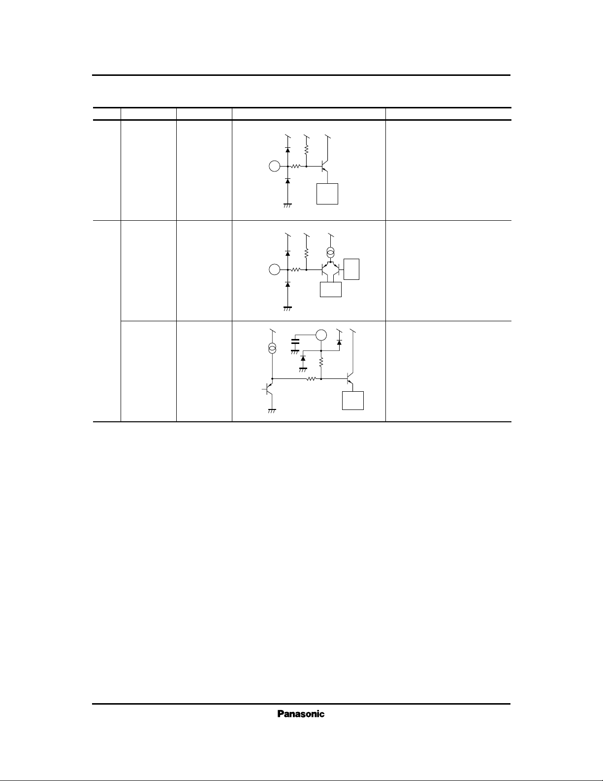
Pin name Equivalent circuit
1
V
CC1
200
Ω
DC voltage (VCC=5V)
Description
2
2
3
9
10
16
CHARGE
Rec. AGC
Det.
DUMP3
DUMP4
DUMP1
DUMP2
1
5kΩ
1.65V
(PB)
1.25V
(PB)
5V
5kΩ
V
CC
(5V)
0.1
µF
2
(For
recording)
0.1µF
15k
Ω
15kΩ
200Ω
70kΩ
36kΩ
5kΩ
411EPCOM
SPCOM
2.2V
(Rec)
(For recording)
4
10Ω
10Ω
100Ω100Ω
■ Pin Descriptions
(For
playback)
2
3
(9)
(10)
(16)
(11)
Power supply input for playback
and recording amplifiers
Integration output of automatic
tracking interface peak detection
signal for the playback mode. An
external capacitor is connected to
this pin for integration function.
Recording AGC detection. Connected to an external capacitor for
the recording mode
Head amplifier damping adjustment. Connected to an external
resistor
Recording current output for the
recording mode. Pin4 (EPCOM) is
terminated in the SP mode, and
Pin11 (SPCOM) is terminated in
the EP mode.
Page 6

6
ICs for VCR
AN3389SB
6
5
7
12
14
GND1
CH3
CH4
CH1
CH2
0.69V
(PB)
15kΩ
(For playback)
5
7
12
14
CH3
CH4
CH1
CH2
2.2V
(Rec)
0V
5
6
50kΩ
20Ω
20Ω
150Ω 100Ω
8 REF 3.2V
13 GND2 0V
8
13
5kΩ
5kΩ 24kΩ
5
( 7 )
(12)
(14)
(For recording)
( 7 )
(12)
(14)
Pin No.
Pin name Equivalent circuit
DC voltage (VCC=5V)
Description
■ Pin Descriptions (cont.)
Playback amplifier input for the
playback mode
Recording current output for the
recording mode
Ground for playback and recording
amplifiers in the EP mode
Reference voltage output for playback amplifiers
Ground for playback and recording
amplifiers in the SP mode
Page 7

7
ICs for VCR
AN3389SB
15 HOLD
200Ω
15
17
18
19
MIN
DCFB
AGCTL
VGCTL
AUDIO
-IN
2.5V for
playback,
and
0.7V for
recording
2.2V
(Rec)
1.25V
(PB)
0.1µF
15
(For
recording)
20
MUTE
SW
2.5V
2.5V
(For playback)
15
0.1µF
100
Ω
100Ω
150Ω
17
18
19
20
46KΩ
46KΩ
2.8KΩ
2.8KΩ
(For
playback)
20kΩ
200Ω
(For
recording)
20kΩ
25k
Ω
25k
Ω
10kΩ
200Ω
Pin No.
PIn name Equivalent circuit
DC voltage (VCC=5V)
Description
■ Pin Descriptions (cont.)
Peak hold of automatic tracking
interface peak detection integration
signal for the playback mode. An
external capacitor is connected to
this pin for peak hold function.
Gain control of automatic tracking
interface amplifiers.Pin17(AGCTL)
controls the gain in the audio mode,
and Pin18 (VGCTL) controls the
gain in the video mode.
Mute control for the recording
mode. Muting is on at low and OFF
at high (open).
Connecting to an external capacitor
for recording amplifier DC voltage
feedback at the recording mode
Automatic tracking interface audio
FM signal input
Page 8

8
ICs for VCR
AN3389SB
22
SYNC
200Ω
23
24
25
DFF IN
DFF OUT
EPSPSW
22
50kΩ
23
24
25
200Ω
20kΩ
200Ω
5V
21
PBCONT
21
20kΩ
200Ω
20Ω
(For playback)
20kΩ
Pin No.
Pin name Equivalent circuit
DC voltage (VCC=5V)
Description
■ Pin Descriptions (cont.)
Playback mode control. Manual,
auto, or still/slow mode is selected
when this pin is high, middle, or
low respectively. Pin36 selects still
or slow mode.
SYNC signal input. Recording
AGC operates when this pin is high.
DRUM.FF signal input
Color rotation control signal output.
This pin goes low when + azimuth
head (ch1 or ch3) is selected, and
goes high when – azimuth head
(ch2 or ch4)is selected.
EP/SP mode selection control.
The EP mode is selected when this
pin is high, and the SP mode is
selected when this pin is low.
Page 9

9
ICs for VCR
AN3389SB
27 GND3
28
29
30
FM OUT
V
CC2
ICC ADJ
Rec AGC
ADJ
Ground
Playback amplifier output
V
CC
3.4V
26 AT OUT
26
4.8kΩ
200Ω
420Ω
0.1V
0V
5V
3.2V for
playback
27
28
29
VCC (5V)
200Ω
30
Pin No.
Pin name Equivalent circuit
DC voltage (VCC=5V)
Description
■ Pin Descriptions (cont.)
Peak hold voltage output of automatic tracking interface peak detection integration signal for the playback mode. In the recording mode,
this pin is forcibly terminated.
Recording amplifier idle-current
control as well as recording AGC
level control
Page 10

10
ICs for VCR
AN3389SB
31 AGC IN
200Ω
32
32
33
AGC Det.
PLUS DCFB
AGC OUT
PB Rec SW
AGC amplifier input
3.1V for
playback
3.6V for
playback
0.1µF
31
34 Rec IN
2.2V for
recording
Recording signal input
(For playback)
32
32
400Ω6kΩ
0.1µF
100
Ω 100Ω
33
34
50kΩ
5kΩ
200Ω
3V
Pin No.
Pin name Equivalent circuit
DC voltage (VCC=5V)
Description
■ Pin Descriptions (cont.)
AGC amplifier detection. Connected to an external capacitor
Connecting to an external capacitor
for recording amplifier DC voltage
feedback for the recording mode.
AGC amplifier output as well as
playback/recording mode selection
control. Recording mode is selected
when this pin is low.
Page 11
11
ICs for VCR
AN3389SB
35 VASEL
200Ω
36
SLOW SW
Rec EQ
Recording equalization
5V
35
3.7V for
recording
50kΩ
36
50kΩ
200Ω
5V for
playback
200Ω
960Ω
36
Pin No.
Pin name Equivalent circuit
DC voltage (VCC=5V)
Description
■ Pin Descriptions (cont.)
Video/audio mode-selection control
for automatic tracking interface.
Video mode is selected when this
pin is high (open), and audio mode
is selected when this pin is low.
Still/slow mode selection control.
Still mode is selected when this pin
is high (open), and slow mode is
selected when this pin is low, under
the condition that Pin21
(PB CONT) is low.
 Loading...