

Page 1
ICs for VCR
■ Overview
The AN3370K can amplify high-frequency current generated by the built-in oscillator and drive the Flying-erase
head. This IC also allows to set an oscillation frequency
and an output current optionally with external constants
according to the erase head.
■ Features
•
Built-in high-accuracy, stable oscillator.
•
Capable of varying output current value and an oscillation frequency with external constants.
AN3370K
Flying-Erase IC
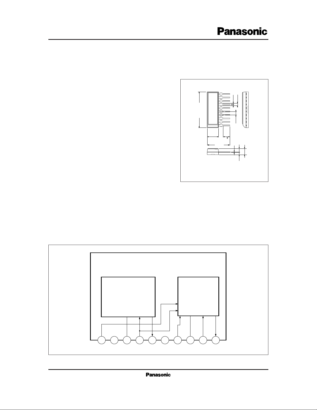
■ Block Diagram
10
1.1±0.25
1.65±0.25
0.25
3.0±0.3
3.5±0.25
0.5
1.1
1.778
+ 0.1
– 0.05
Unit : mm
1
10-Pin Shrunk SIL Plastic Package (10-SSIP)
6.0±0.3
(12.0)
18.24±0.3
Output
Driver
1 2 3 4 5 6 7 8 9 10
V
CC
GND
OSC
Page 2
ICs for VCR
AN3370K
V
O1
f
O
V1= 5V, RL= 300Ω
V
1
= 5V, RL= 300Ω
Supply current
Oscillation output amplitude
Oscillation frequency
8
11911.55 12.1
V
PP
MHz
Parameter minCondition typ max UnitSymbol
V
O2
V1= 0V, RL= 300Ω
Oscillation output amplitude
10 mV
PP
V
1H
Flying ON
3.5 V
V
1L
Flying OFF
0.8 V
I
CC
V1= 5V 20 28 36 mA
■ Electrical Characteristics (VCC=12V, Ta=25˚C)
1 2 3 4 5 6 8 107
1.8kΩ
0.01µF
V
CC=12V
0.01
µF
4µH
68pF
68pF
56pF
100µF
4.7µH
33pF
0.01µF
5.1kΩ
Output
Driver
OSC
9
Flying Control Voltage
Note) Do not apply a voltage (0V included) to the Pin2 from the external.
Parameter Symbol Rating Unit
V
CC
P
D
T
opr
T
stg
Power dissipation
Supply voltage
Operating ambient temperature
Storage temperature
12.6
500
– 20 to + 70
– 55 to +150
V
mW
˚C
˚C
■ Absolute Maximum Ratings (Ta=25˚C)
Parameter Symbol Range
Operating supply voltage range
V
CC
10.5V to 12.5V
■ Recommended Operating Range (Ta = 25˚C)
■ Application Circuit
Page 3

ICs for VCR
AN3370K
Pin No.
Pin name
Description
I/O
impedance
Equivalent circuit
Typ. waveform
1
2
3
4
5
6
7
8
9
10
Power supply
Output pin
GND
Oscillation
input pin
Reference
voltage pin
Oscillation
feedback pin
Oscillation
output pin
High-frequency current
3MΩ
60kΩ
10kΩ
NPN T
r
emitter
NPN T
r
emitter
3kΩ
6.2kΩ
6V
3.4V
6V
1
30kΩ
30kΩ
2
30kΩ
30kΩ
5
3
5
3
10kΩ
10kΩ
7
2V
6V
8
9
3kΩ
10
6.2kΩ
8
Flying erase
control pin
Flying erase ON/OFF control pin.
ON when 3.5V or more is applied,
and OFF when 0.8V or less is
applied.
Feedback pin to obtain a DC voltage by filtering an output signal
via an external capacitor
Do not apply a voltage from the
external.
Power supply pin.
Apply 12V typically from the
external.
Generates a reference voltage of
1/2 VCC (approx. 6V)
A signal from Pin10 oscillation
output is divided by the capacitor
and is fed back.
Oscillates at the frequency determined by L, C of the Pins8, 9, 10
It is possible to change the current
which can be taken out of an output, by varying the resistor
between this pin and GND.
Feedback pin
■ Pin Descriptions
Page 4

ICs for VCR
AN3370K
1 2 3 4 5 6 7 98 10
0.01µF
V
CC=12V
V
H= 5V
0.01µF
100µF
4.7µH
C1
C2
RX
0.01µF
L
X
CX1 CX2
AN3370K
Flying Erase
H
Erase Head L
■ Supplementary Explanation
• Characteristic Curve
1) Internal Oscillation Frequency
An internal oscillation frequency is determined by the following expression. Set CX1, CX2, and LX according to a frequency.
In order to obtain stable oscillation, set CX1/CX2 near 1 and
absolute value of CX1, CX2 to such a considerable extent that
an internal IC capacitance (approx. 5pF) and an external
PCB capacitance can be ignored.
2) R
X
Output current amplitude from the IC is determined by the
external resistor RX of the Pin7 ; it is approximately as
shown in Fig. 1. Therefore, use within the following range.
I5=20mApp to 65mApp.
3) Do not apply the Pin1 voltage when VCC is off.
Use the Pin2 voltage open.
4) Output Dynamic Range
Since the output pin (5) dynamic range of the AN3370K is
8VPP (at VCC=12V), set a combination of C1, C2, and erase head
inductance (L) so that the following will be ensured.
I5 (mApp)
× load impedance < 8VPP.
5) Serial and Parallel Resonance Points
• Serial resonance
frequency
Since Pin5 amplitude is minimized at a point of f1, set f1
so that it will almost coincide with f
OSC
.
• Parallel resonance frequency
Suppose the internal capacitance of the Pin5 is
C5, then parallel resonance frequency is
Although an erase head current is maximized at this point,
set f2/f
OSC
= 1.25 to 1.4
f
OSC
=
1
Lx·
CX1 · C
X2
CX1+ C
X2
2π
·················(1)
f
1
=
1
L (C1 + C2)
2π
(2)
f
2
=
L
2π
· · · (3)
L
C5 · C
1
C5 + C
1
C2 +
Fig. 1.
.
.
· · ·······
I5–R
X
I
5
(mA
PP
)
RX (kΩ)
0 5 10 15 20 25
0
20
40
60
80
100
VCC=12V
L
X
= 5.6µH
C
X1
= CX2= 68pF
fosc=10.8MHz
I
50Ω R
X
0.047µF
5
5
7
 Loading...