

Page 1
ICs for VCR
AN3358SH
2-head recording and playback amplifier IC for 8 mm video camera
■ Overview
The AN3358SH is a recording and playback amplifier IC for 8 mm video camera of 2-head large diameter
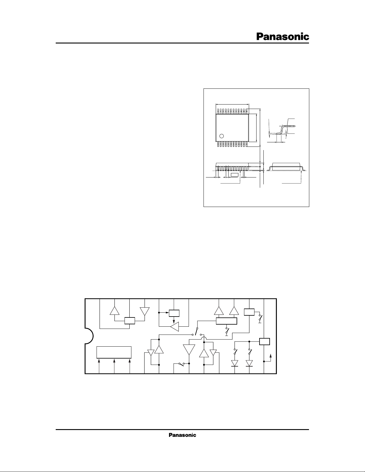
cylinder, and encapsulated in a small SO package of 24
pins and 0.5 mm pitch.
■ Features
• 2-channel playback head amp
• 2-channel recording amp (collector open type
with a single pin output)
• RF-AGC
• Pulse generator for drop out compensation
(DOC)
• Supply voltage: 5 V ± 0.5 V
• Small SO package of 0.5 mm pitch (SSOP-24D)
■ Applications
• 8 mm video camera
■ Block Diagram
6.5 ± 0.3
24 13
112
0.50
(0.50)
Seating plane
0.2 ± 0.1
SSOP024-P-0300A
5.5 ± 0.3
7.5 ± 0.3
0.65 ± 0.100.65 ± 0.10
1.5 ± 0.20.1 ± 0.1
0
.1
0
+
(0.50)
5
.0
0
−
0.15
Unit: mm
0° to 10°
Seating plane
24
1
HSW
23
LOGIC
2
DOC out
PB/REC
22
Det
3
Mute/REC
DOC in
AGC out
20
21
Det
ch.1
4
5
CH1 HA in
19
6
GND
AGC in
18
HL
7
8
GND
17
ch.2
Y-out
16
Diff
9
CH2 HA in
ATF out
15
10
V-Reg out CH1
Y/C/ATF/Aud. in
14
Buff.
11
V-Reg out CH2
13
Reg
12
CC
V
1
Page 2
AN3358SH ICs for VC R
■ Pin Descriptions
Pin No. Description
1 HSW changeover pin
2 PB/REC changeover pin
3 Mute/REC changeover pin
4 ch.1 head amp. damping pin
5 ch.1 head amp. input pin
6 Small signal GND
7 REC curr. amp. output pin
8 ch.2 head amp. input pin
9 ch.2 head amp. damping pin
10 V-reg out.ch.2 pin
11 V-reg out.ch.1 pin
12 Main V
CC
■ Absolute Maximum Ratings
Parameter Symbol Rating Unit
Supply voltage V
Supply current I
2
Power dissipation
Operating ambient temperature
Storage temperature
Note)*1: Except for the operating ambient temperature and storage temperature, all ratings are for Ta = 25°C.
2: The power dissipation shown is for the IC package in free air at Ta = 70°C.
*
*
1
*
1
*
CC
CC
P
D
T
opr
T
stg
Pin No. Description
13 Capacitor pin for V-Reg.
14 REC curr. amp. input pin
15 ATF output pin
16 Y-output pin
17 Main GND
18 AGC input pin
19 AGC det pin
20 AGC output pin
21 DOC input pin
22 DOC det pin
23 DOC output pin
24 DOC level control pin
6V
mA
201 mW
−20 to +70 °C
−55 to +125 °C
■ Recommended Operating Range
Parameter Symbol Range Unit
Supply voltage V
CC
■ Electrical Characteristics at Ta = 25°C
Parameter Symbol Conditions Min Typ Max Unit
REC circuit current I
Recording current output I
PB/REC V
12RECVCC
7
2RECVCC
REC mode hold voltage measurement
Mute/REC V
3RECVCC
REC mode hold voltage measurement
Mute/REC V
3MuteVCC
Mute mode hold voltage measurement
PB circuit current I
12PB
2
= 5 V 29 (41) 53 mA
V
= 5 V,V
CC
f = 5 MHz
= 5 V, pin 2 potential 0 1.5 V
= 5 V, pin 3 potential 0 1.5 V
= 5 V, pin 3 potential 3.5 5V
V
= 5 V 12 (17) 22 mA
CC
4.5 to 5.5 V
= 200 mV[p-p], 31 (44) 57 mA[p-p]
IN
Page 3
ICs for VCR AN3358SH
■ Electrical Characteristics at Ta = 25°C (continued)
Parameter Symbol Conditions Min Typ Max Unit
HSW DC unbalance HSW VCC = 5 V 100 mV[p-p]
ch.1 gain G
ch.2 gain G
Y-output/ATF output gain ratio G
−G
Input-referred noise ch.1 N
G
Input-referred noise ch.2 N
G
ATF output DC voltage V
Y-output DC voltage V
PB/REC PB mode hold voltage V
HSW high-level hold voltage V
HSW low-level hold voltage V
AGC output amplitude V
AGC sensitivity ∆V
AGC output DC voltage V
Drop-out detection on level V
Drop-out detection off level V
Drop-out pulse low-level V
Drop-out pulse high-level V
Recording current secondary D
harmonic distortion
Recording current frequency I
characteristics ratio
*
*
7H
PB frequency characteristics V
*
ratio
Note) The standard values in the parenthesis are the typical values and not the guaranteed ones.
V
VCC = 5 V, 60 (64) 68 dB
5-16
pin 5 input: V
= 0.3 mV[p-p]
IN
f = 5 MHz
V
8-16
= 5 V, 60 (64) 68 dB
CC
pin 8 input: V
= 0.3 mV[p-p]
IN
f = 5 MHz
V
5-16
5-15
= 5 V,
CC
pin 5 input: V
= 0.3 mV[p-p] −2 (0) 2 d B
IN
f = 5 MHz
/VCC = 5 V, 1 MHz BPF output is 1
5-16
divided by gain
5-16
/VCC = 5 V, 1 MHz BPF output is 1
8-16
divided by gain
8-16
VCC = 5 V 1.9 (2.3) 2.7 V
15
VCC = 5 V 1.9 (2.3) 2.7 V
16
VCC = 5 V, pin 2 potential 3.5 5V
2PB
measurement
V
1H
= 5 V, pin 1 potential 3.5 5V
CC
measurement
V
1L
= 5 V, pin1 potential 0 1.5 V
CC
measurement
18-20
VCC = 5 V,V
= 500 mV[p-p], 280 (400) 520
IN
f = 5 MHz
18-20VCC
= 5 V, f = 5 MHz 3dB
VIN = 500 mV[p-p] ± 6 dB
V
20
21ONVCC
= 5 V 2.05 (2.45) 2.85 V
CC
= 5 V, f = 5 MHz, −16.0 (−12.5) −10.5 dB
VIN = 400 mV[p-p] → 0
21OFFVCC
23L
= 5 V, f = 5 MHz, −9.5 (−7.5) −5.5 dB
V
= 0 → 400 mV[p-p]
IN
V
CC
= 5 V,V
= 400 mV[p-p], (0) 0.5 V
IN
f = 5 MHz
VCC = 5 V 2.8 (3.2) 3.6 V
23H
VCC = 5 V, VIN = 200 mV[p-p], −45 dB
2f
f = 5 MHz
/ IZV
/V
16H
16
= 5 V, f = 10 MHz, 5 MHz 0 dB
CC
V
= 200 mV[p-p]
IN
= 5 V, f = 10 MHz, 5 MHz −3 dB
CC
VIN = 0.3 mV[p-p]
µV[rms]
µV[rms]
mV[p-p]
3
Page 4

AN3358SH ICs for VC R
■ Terminal Equivalent Circuits
Pin No. Equivalent Circuit Description Pin Voltage Remark
1 HSW High: ch.1 output Set the outputting
150
µA
23 kΩ
1
V
CC
30 kΩ30 kΩ
changeover pin (Pin 5 input) channel by pin 1.
Ch.1 is outputted at
open.
Low: ch.2 output
2.5 V
(Pin 8 input)
2 PB/REC High: PB PB and REC
300
µA
V
CC
changeover pin Low: REC modes are changed
by pin 2.
23 kΩ
(or mute) PB mode at open.
Select mute or
2.5 V
REC by pin 3.
2
3 Mute/REC High: mute Select mute or
300
µA
V
CC
changeover pin Low: REC REC by pin 3.
Mute mode at open.
23 kΩ
2.5 V
3
4 ch.1 head amp.
V
CC
damping pin REC 2.1 V
Mute 1.4 V
7.5 kΩ
5
4.5 kΩ
1.25 V
4
PB 1.4 V
5 ch.1 head amp.
input pin REC GND
Mute 0.7 V
7.5 kΩ
5
4.5 kΩ
PB 0.7 V
4
Page 5

ICs for VCR AN3358SH
■ Terminal Equivalent Circuits (continued)
Pin No. Equivalent Circuit Description Pin Voltage Remark
6 Small signal GND
7 REC curr. amp.
7810 115
16.7 Ω
8 ch.2 head amp.
7.5 kΩ
8
10 Ω10 Ω
4.5 kΩ
V
CC
output pin REC 4 V
Mute GND
PB GND
input pin REC GND
Mute 0.7 V
PB 0.7 V
9 ch.2 head amp.
7.5 kΩ
4.5 kΩ
8
V
CC
1.25 V
damping pin REC 2.1 V
9
10 V-reg out
V
CC
ch.2 pin REC 4.2 V
10
20 kΩ
Mute 1.4 V
PB 1.4 V
Mute GND
PB GND
5
Page 6

AN3358SH ICs for VC R
■ Terminal Equivalent Circuits (continued)
Pin No. Equivalent Circuit Description Pin Voltage Remark
11 V-reg out
V
CC
ch.1 pin REC 4.2 V
Mute GND
11
20 kΩ
12 Main V
CC
13 For V-reg
V
100 kΩ
200
CC
46.6 kΩ
1.2 mA
Ω
capacitor pin REC 4.2 V
13
14 REC curr. amp.
V
1 mA
1 mA
CC
0.01 µF
14
input pin REC 1.6 V
PB GND
Mute 5 V
PB 5 V
Mute 1.6 V
PB GND
15 ATF output pin
V
CC
200 Ω
1 kΩ
15
200 µA 1 mA
6
REC 4.1 V
Mute 4.1 V
PB 2.3 V
Page 7

ICs for VCR AN3358SH
■ Terminal Equivalent Circuits (continued)
Pin No. Equivalent Circuit Description Pin Voltage Remark
16 Y-output pin
V
CC
200 Ω
1 kΩ
16
200 µA 1 mA
17 Main GND
18 AGC input pin
V
CC
REC 4.1 V
Mute 4.1 V
PB 2.3 V
REC 2.4 V
3.7 V
30
kΩ
30
kΩ
18
100
µA
12 kΩ
100
µA
50 µA
50
µA
50
µA
19 AGC det. pin
V
19.5 kΩ
80
Ω
3.75
kΩ
100
µA
3.5 V
1.5 kΩ
27.6
kΩ
80 Ω
19
CC
1.5 kΩ
50 µA
20 AGC output pin
V
CC
80 Ω
750 Ω
20
100 µA 400 µA
Mute 2.4 V
PB 3 V
REC 3.2 V
Mute 2.9 V
PB 2.9 V
REC 4.4 V
Mute 4.4 V
PB 2.45 V
7
Page 8

AN3358SH ICs for VC R
■ Terminal Equivalent Circuits (continued)
Pin No. Equivalent Circuit Description Pin Voltage Remark
21 DOC input pin
V
20
kΩ
CC
30
3 V
kΩ
20
pF
30
kΩ
21
100
µA
1 kΩ
150 µA
22 DOC det. pin
10 kΩ
15
kΩ
200
4 kΩ
150 µA
Ω
22
100 µA 150 µA
150
30
kΩ
100 µA
µA
V
CC
11.1 kΩ
23 DOC output pin
200 Ω
23
32.5 kΩ
REC 4.4 V
Mute 4.4 V
PB 2.4 V
REC GND
Mute GND
3.2 V
PB GND
24 DOC level
3 kΩ
9 kΩ
6 kΩ
3 kΩ
24
V
CC
control pin REC 2.25 V
8
Mute 2.25 V
PB 2.25 V
Page 9

ICs for VCR AN3358SH
■ Application Circuit Example
Y-in
C-in
ATF in
Audio in
24
1
HSW
23
LOGIC
2
PB/REC
DOC out
22
Det
3
Mute/REC
100 pF
+
0.47 µF50 Ω
DOC in
AGC out
19
20
21
Det
ch.1
4
5
6
0.01 µF
0.01 µF
AGC in
0.1 µF
0.01 µF
18
HL
7
150 Ω
0.01 µF
8
17
ch.2
Y-out
16
Diff
9
+
0.01 µF 560 Ω
0.01 µF 560 Ω
0.01 µF 560 Ω
0.01 µF 560 Ω
ATF out
15
Buff.
10
0.47 µF
50 Ω
4.3 kΩ
13
14
Reg
11
12
100 µH
+
0.01 µF
47 µF
5 V
CC
V
9
 Loading...