

Page 1
ICs for VCR
AN3328S
2-head recording and playback amplifier IC (A2) for HiFi VCR
■ Overview
The AN3328S is a 2-head recording and playback amplifier IC for HiFi audio, and realized
reduction of pin numbers. The package is a small
outline of 16 pins, 1.27 mm pitch and supply voltage is 5 V of single supply.
■ Features
• Damping-less amp. in playback system
• No adjustment of recording current by AGC
• 3-step switchover of recording current level with
the current emphasis switch (typ. ± 1.8 dB)
■ Applications
• HiFi VCR
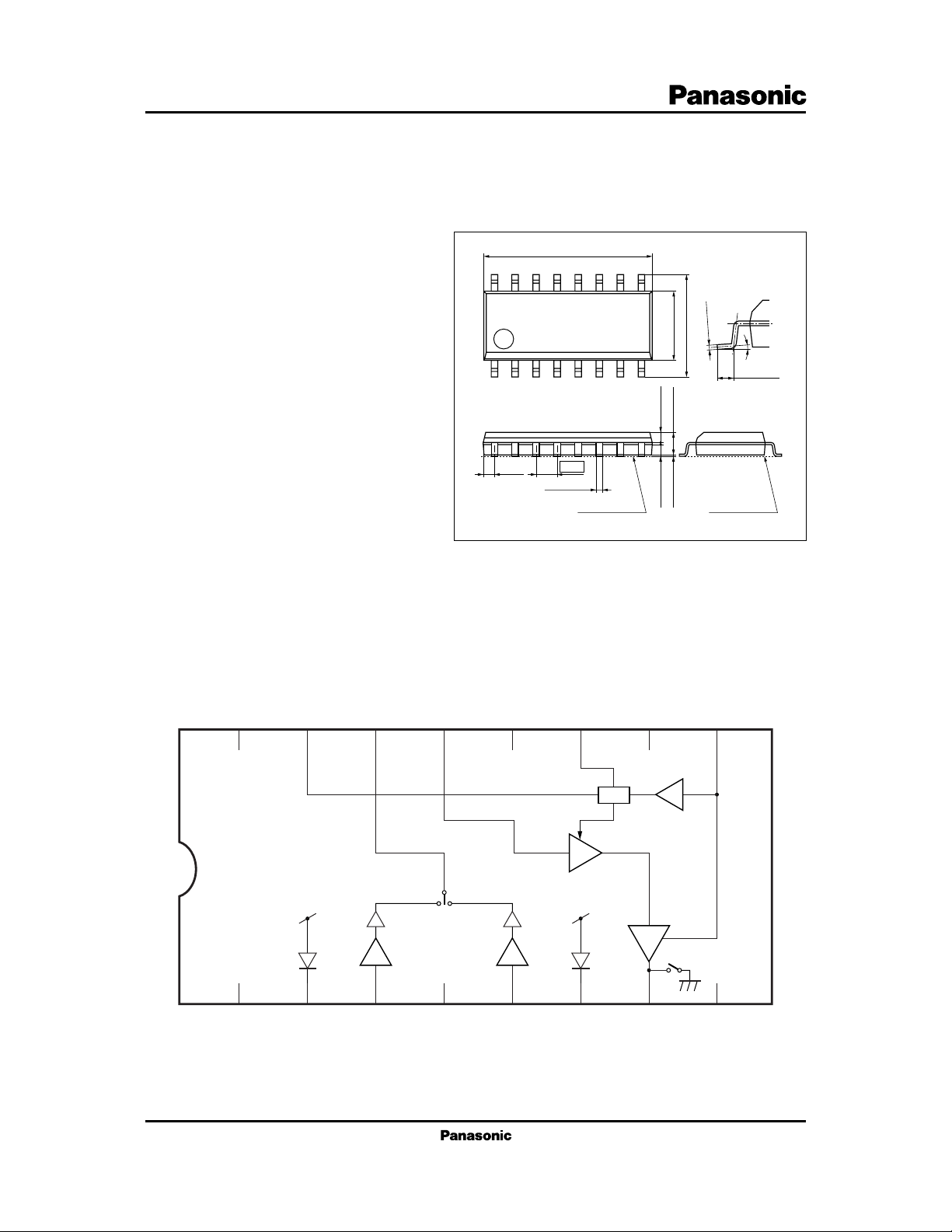
■ Block Diagram
−0.05
+0.10
0.15
Seating plane
Unit: mm
0° to 10°
0.50 ± 0.20
10.09 ± 0.20
16 9
4.30 ± 0.20
6.40 ± 0.30
18
0.65 ± 0.100.65 ± 0.10
1.50 ± 0.200.10 ± 0.10
(0.60)
1.27
0.40 ± 0.10
Seating plane
SOP016-P-0225C
REC / PB selectHSW
16
1
REC C
15
2
REC reg1
PB out &
REC / mute
14
HA1 HA2
3
CH1 in
REC in
13
LH
4
GND (small signal)
GND
12
5
CH2 in
11
AGC
6
REC reg2
Det
V
10
Curr.
Amp.
7
REC out
CC
REC curr. monitor
9
8
Curr. emph. SW
1
Page 2
AN3328S ICs for V CR
■ Pin Descriptions
Pin No. Description
1 Audio head SW
2 REC regulator1
3 Head amp. input ch.1
4 GND (small signal)
5 Head amp. input ch.2
6 REC regulator2
7 REC out
8 Curr. emph. SW
Pin No. Description
9 REC curr. monitor (control)
10 V
CC
11 REC AGC det
12 GND
13 REC input
14 PB out & REC / mute SW
15 REC C
16 REC/PB select SW
■ Absolute Maximum Ratings
Parameter Symbol Rating Unit
Supply voltage V
Supply current I
Power dissipation
Operating ambient temperature
Storage temperature
Note)*1: Except for the operating ambient temperature and storage temperature, all ratings are for Ta = 25°C.
2: The power dissipation shown is for the IC package in free air at Ta = 70°C.
*
*2
*1
*1
CC
CC
P
D
T
opr
T
stg
6V
mA
240 mW
-20 to +70 °C
-55 to +125 °C
■ Recommended Operating Range
Parameter Symbol Range Unit
Supply voltage V
CC
4.5 to 5.5 V
2
Page 3
ICs for VCR AN3328S
■ Electrical Characteristics at Ta = 25°C
Parameter Symbol Conditions Min Typ Max Unit
REC I
10(REC)
Circuit current REC / PB SW: High
REC I
AGC level REC / PB SW: High
REC DI
AGC control characteristics REC / PB SW: High
REC Recording current D
2nd harmonic distortion VIN = 260 mV[p-p], 2 MHz
REC V
Mode hold voltage VIN = 260 mV[p-p], 2 MHz
REC V
Over REC hold voltage REC / PB SW: High
REC V
Normal hold voltage REC / PB SW: High
REC V
S-VHS hold voltage REC / PB SW: High
REC I
7L
Over REC current ratio REC / PB SW: High
REC I
7H
S-VHS current ratio REC / PB SW: High
REC V
14H(REC)VCC
Mute hold voltage 1 REC / PB SW: High
REC V
14L(REC)VCC
Mute hold voltage 2 REC / PB SW: High
PB I
10(PB)
Circuit current REC / PB SW: Low
PB G
CH1 gain HSW: High, VIN = 0.1 mV[p-p], 2 MHz
PB G
CH2 gain HSW: Low, VIN = 0.1 mV[p-p], 2 MHz
PB DG
CH1 1.5 M / 2 M gain ratio HSW: High, VIN = 0.1 mV[p-p], 2 MHz
PB DG
CH2 1.5 M / 2 M gain ratio HSW: Low, VIN = 0.1 mV[p-p], 2 MHz
PB G
3-14
CH1 / CH2 gain ratio G
Noise referred to PB N
CH1 input REC / PB SW: Low HSW: High
Noise referred to PB N
CH2 input REC / PB SW: Low HSW: Low
Note) The typical value in the parenthesis is not the guaranteed one.
VCC = 5.0 V 56 (66) 76 mA
V
7
7
7
16H
8L
8M
8H
= 5.0 V 44 (48) 52
CC
VCC = 5.0 V (0.2) 1.0 dB
VCC = 5.0 V, REC / PB SW: High (−43) −35 dB
VCC = 5.0 V, REC / Mute SW: Low 3.6 Vcc V
VCC = 5.0 V 0 1.2 V
VCC = 5.0 V 1.8 3.2 V
VCC = 5.0 V 3.8 Vcc V
mA[p-p]
→ I7VCC = 5.0 V 1.3 (1.8) 2.3 dB
→ I7VCC = 5.0 V −2.3 (−1.8) −1.3 dB
= 5.0 V 3.6 Vcc V
= 5.0 V 0 1.4 V
VCC = 5.0 V 9 (13) 17 mA
VCC = 5.0 V, REC / PB SW: Low 72 (76) 80 dB
3-14
VCC = 5.0 V, REC / PB SW : Low 72 (76) 80 dB
5-14
VCC = 5.0 V, REC / PB SW: Low 0 (0.5) 1 dB
3-14
VCC = 5.0 V, REC / PB SW: Low 0 (0.5) 1 dB
5-14
→ VCC = 5.0 V, REC / PB SW: Low −20 2dB
5-14VIN
3-14
5-14
= 0.1 mV[p-p], 2 MHz
VCC = 5.0 V 1.0
VCC = 5.0 V 1.0
mV[rms]
mV[rms]
3
Page 4

AN3328S ICs for V CR
■ Electrical Characteristics at Ta = 25°C (continued)
Parameter Symbol Conditions Min Typ Max Unit
PB V
Mode hold voltage REC / PB SW: Low
PB V
1H(PB)VCC
CH1 hold voltage REC / PB SW: Low
PB V
1L(PB)
CH2 hold voltage REC / PB SW: Low
PB
DV
OFFSETVCC
HSW DC unbalanced REC / PB SW: Low
• Design reference data
Note) The characteristics listed below are theoretical values based on the IC design and are not guaranteed.
Parameter Symbol Conditions Min Typ Max Unit
REC Cross modulation CMD
distortion at 0.4 MHz REC / PB SW: High
REC Cross modulation CMD
distortion at 0.9 MHz REC / PB SW: High
REC I
M
Muting ratio REC / PB SW: High
PB CT
Crosstalk CH1 to CH2 REC / PB SW: Low
PB CT
Crosstalk CH2 to CH1 REC / PB SW: Low
PB CH1, Output 2nd D
harmonic distortion REC / PB SW: Low
PB CH2, Output 2nd D
harmonic distortion REC / PB SW: Low
Note) The typical value in the parenthesis is not the guaranteed one.
VCC = 5.0 V 0 1.4 V
16L
= 5.0 V 3.6 V
CC
V
VCC = 5.0 V 0 1.4 V
0.4MVCC
0.9MVCC
= 5.0 V 20
= 5.0 V (−45) dB
= 5.0 V (−52) dB
mV[p-p]
/ I7VCC = 5.0 V −40 dB
VCC = 5.0 V −40 dB
1
VCC = 5.0 V −40 dB
2
VCC = 5.0 V, HSW: High −50 dB
3-14
VCC = 5.0 V, HSW : Low −50 dB
5-14
4
Page 5

ICs for VCR AN3328S
0.7 V
0.7 V
■ Terminal Equivalent Circuits
Pin No. Equivalent Circuit Description Voltage Remark
1 Audio head SW Input signal At open :
5 V
0 V
3 kΩ 3 kΩ
2.5 V
23 kΩ
1
3 kΩ
2 REC regulator 1 D.C
46.6 kΩ
High
(ch.1 Select)
REC: ON
2
101.2 kΩ18 kΩ
3 Head amp. input
2.1 V
3
1.125 kΩ
380 Ω
15 kΩ
6 kΩ
ch.1
4 GND (small signal)
5 Head amp. input
ch.2
2.1 V
1.125 kΩ
380 Ω
6 kΩ
5
15 kΩ
5
Page 6

AN3328S ICs for V CR
■ Terminal Equivalent Circuits (continued)
Pin No. Equivalent Circuit Description Voltage Remark
6 REC regulator 2 D.C
46.6 kΩ
REC: ON
6
18 kΩ
101.2 kΩ
7 REC out A.C
750 Ω
7
9 REC curr. monitor
(control)
9
200 Ω
800 Ω
8 Curr. emph. SW Input signal At open:
Middle
75 kΩ 45 kΩ
23 kΩ
9 kΩ
5 V
(Curr. emph.
normal mode)
2.5 V
69 kΩ
3.5 V
0 V
23 kΩ
75 kΩ
8
69 kΩ
1.5 V
10 V
CC
11 REC AGC det D.C
200 Ω200 Ω
20
12 GND
6
Page 7

ICs for VCR AN3328S
■ Terminal Equivalent Circuits (continued)
Pin No. Equivalent Circuit Description Voltage Remark
13 REC input
10.5 kΩ
2.7 V
20 kΩ
12 kΩ
200 Ω
13
20 kΩ
2.7 V
2 V
14 PB out & At open: Low
1.8 V
OFF)
Input signal
4.3 V
3 kΩ
1.8 kΩ
80 Ω
REC / mute SW (REC Mute
46 kΩ
200 Ω
2.5 V
14
69 kΩ
1.8 V
15 Audio REC D.C
1.5 kΩ
1.5 kΩ
capacitor
6k Ω
200 Ω
10.7k Ω
500 Ω
200 Ω
15
16 REC / PB Input signal At open: Low
select SW (PB-Mode)
4.5kΩ
5 V
0 V
16
23 kΩ
100 kΩ
69 kΩ
100 Ω100 Ω
69 kΩ
2.5 V
7
Page 8

AN3328S ICs for V CR
■ Application Circuit Example
REC / PB LowHSW
16
1
REC/mute High
FM out
3.3µF
15
2
14
HA1 HA2
3
0.01 µF
FM in
13
4
0.01 µF
0.01 µF
12
LH
5
0.01 µF
11
AGC
6
0.01 µF
10
Det
Curr.
Amp.
7
100 Ω
100µH
47 µF
9
8
0.01 µF
Curr. emph. SW
V
CC
5 V
12 Ω
8
 Loading...