

Page 1
AN3233
Application note
12 V - 150 W resonant converter with synchronous rectification
using the L6563H, L6599A, and SRK2000
Introduction
This application note describes the characteristics and features of a 150 W SMPS
demonstration board (EVL150W-ADP-SR), tailored to all-in-one computer power supply
(PS) specifications.
The characteristics of this design are the very high efficiency and low consumption at light
load which make it a viable solution for applications compliant with ENERGY STAR
eligibility criteria (EPA rev. 5.0 computer and EPA rev. 2.0 EPS). One of the key factors to
achieving high efficiency at heavy load is the SRK2000. This synchronous rectification (SR)
driver for LLC resonant converters allows a significant decrease in secondary side losses.
Standby consumption is very low thanks to the sleep function embedded in the SRK2000
and the high voltage start-up circuit integrated in the L6563H. The possibility of driving the
PFC burst mode via the L6599A PFC_STOP pin dramatically boosts light load efficiency.
Additionally, a secondary sensing circuit, dedicated to driving the primary controller into
burst mode, reduces deviation of light load efficiency against resonant circuit parameter
spread, improving the repeatability of design in production volumes.
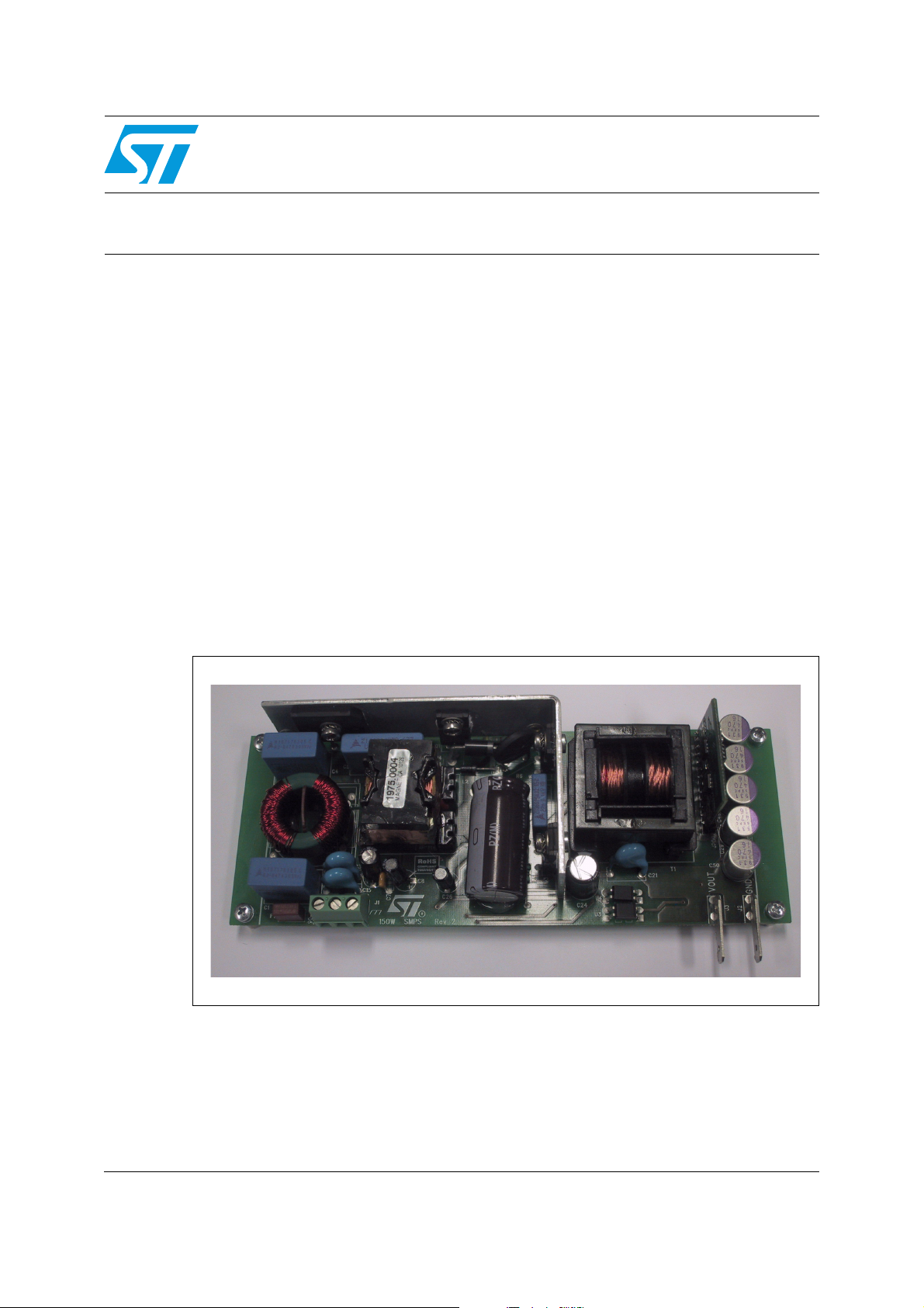
Figure 1. EVL150W-ADP-SR: 150 W SMPS demonstration board
®
January 2011 Doc ID 17595 Rev 1 1/35
www.st.com
Page 2

Contents AN3233
Contents
1 Main characteristics and circuit description . . . . . . . . . . . . . . . . . . . . . 5
2 Efficiency measurement . . . . . . . . . . . . . . . . . . . . . . . . . . . . . . . . . . . . . 11
3 Harmonic content measurement . . . . . . . . . . . . . . . . . . . . . . . . . . . . . . 13
4 Functional check . . . . . . . . . . . . . . . . . . . . . . . . . . . . . . . . . . . . . . . . . . . 14
5 Thermal map . . . . . . . . . . . . . . . . . . . . . . . . . . . . . . . . . . . . . . . . . . . . . . 19
6 Conducted emission pre-compliance test . . . . . . . . . . . . . . . . . . . . . . 21
7 Bill of materials. . . . . . . . . . . . . . . . . . . . . . . . . . . . . . . . . . . . . . . . . . . . . 22
8 PFC coil specification . . . . . . . . . . . . . . . . . . . . . . . . . . . . . . . . . . . . . . . 30
9 Transformer specification . . . . . . . . . . . . . . . . . . . . . . . . . . . . . . . . . . . 32
10 Revision history . . . . . . . . . . . . . . . . . . . . . . . . . . . . . . . . . . . . . . . . . . . 34
2/35 Doc ID 17595 Rev 1
Page 3

AN3233 List of figures
List of figures
Figure 1. EVL150W-ADP-SR: 150 W SMPS demonstration board . . . . . . . . . . . . . . . . . . . . . . . . . . . 1
Figure 2. Burst mode circuit block diagram . . . . . . . . . . . . . . . . . . . . . . . . . . . . . . . . . . . . . . . . . . . . . 7
Figure 3. Electrical diagram . . . . . . . . . . . . . . . . . . . . . . . . . . . . . . . . . . . . . . . . . . . . . . . . . . . . . . . . 10
Figure 4. Light load efficiency diagram . . . . . . . . . . . . . . . . . . . . . . . . . . . . . . . . . . . . . . . . . . . . . . . 12
Figure 5. Compliance with EN61000-3-2 at 230 Vac – 50 Hz, full load . . . . . . . . . . . . . . . . . . . . . . . 13
Figure 6. Compliance with JEITA-MITI at 100 Vac – 50 Hz, full load . . . . . . . . . . . . . . . . . . . . . . . . 13
Figure 7. Resonant stage waveforms at 115 V – 60 Hz – full load . . . . . . . . . . . . . . . . . . . . . . . . . . 14
Figure 8. SRK2000 key signals at 115 V – 60 Hz – full load . . . . . . . . . . . . . . . . . . . . . . . . . . . . . . . 14
Figure 9. High-side MOSFET ZV turn-on at 115 V – 60 Hz – full load. . . . . . . . . . . . . . . . . . . . . . . . 14
Figure 10. Low-side MOSFET ZV turn-on at 115 V – 60 Hz – full load . . . . . . . . . . . . . . . . . . . . . . . . 14
Figure 11. Converter startup at 115 Vac full load . . . . . . . . . . . . . . . . . . . . . . . . . . . . . . . . . . . . . . . . 15
Figure 12. Converter shutdown at 115 Vac full load . . . . . . . . . . . . . . . . . . . . . . . . . . . . . . . . . . . . . . 15
Figure 13. Startup resonant current . . . . . . . . . . . . . . . . . . . . . . . . . . . . . . . . . . . . . . . . . . . . . . . . . . . 15
Figure 14. Shutdown resonant current. . . . . . . . . . . . . . . . . . . . . . . . . . . . . . . . . . . . . . . . . . . . . . . . . 15
Figure 15. No-load operation . . . . . . . . . . . . . . . . . . . . . . . . . . . . . . . . . . . . . . . . . . . . . . . . . . . . . . . . 16
Figure 16. No-load operation – detail. . . . . . . . . . . . . . . . . . . . . . . . . . . . . . . . . . . . . . . . . . . . . . . . . . 16
Figure 17. Transition full load to no load at 115 Vac – 60 Hz . . . . . . . . . . . . . . . . . . . . . . . . . . . . . . . 16
Figure 18. Transition no load to full load at 115 Vac – 60 Hz . . . . . . . . . . . . . . . . . . . . . . . . . . . . . . . 16
Figure 19. Short-circuit at full load and 115 Vac – 60 Hz. . . . . . . . . . . . . . . . . . . . . . . . . . . . . . . . . . . 17
Figure 20. Thermal map at 115 Vac – 60 Hz - full load . . . . . . . . . . . . . . . . . . . . . . . . . . . . . . . . . . . . 18
Figure 21. Thermal map at 230 Vac – 50 Hz - full load . . . . . . . . . . . . . . . . . . . . . . . . . . . . . . . . . . . . 18
Figure 22. Thermal map SR daughterboard - full load. . . . . . . . . . . . . . . . . . . . . . . . . . . . . . . . . . . . . 19
Figure 23. CE average measurement at 115 Vac and full load . . . . . . . . . . . . . . . . . . . . . . . . . . . . . . 20
Figure 24. CE average measurement at 230 Vac and full load . . . . . . . . . . . . . . . . . . . . . . . . . . . . . . 20
Figure 25. PFC coil electrical diagram . . . . . . . . . . . . . . . . . . . . . . . . . . . . . . . . . . . . . . . . . . . . . . . . . 29
Figure 26. PFC coil mechanical aspect . . . . . . . . . . . . . . . . . . . . . . . . . . . . . . . . . . . . . . . . . . . . . . . . 30
Figure 27. Transformer electrical diagram . . . . . . . . . . . . . . . . . . . . . . . . . . . . . . . . . . . . . . . . . . . . . . 31
Figure 28. Transformer overall drawing . . . . . . . . . . . . . . . . . . . . . . . . . . . . . . . . . . . . . . . . . . . . . . . . 32
Doc ID 17595 Rev 1 3/35
Page 4

List of tables AN3233
List of tables
Table 1. Overall efficiency . . . . . . . . . . . . . . . . . . . . . . . . . . . . . . . . . . . . . . . . . . . . . . . . . . . . . . . . 11
Table 2. Light load efficiency . . . . . . . . . . . . . . . . . . . . . . . . . . . . . . . . . . . . . . . . . . . . . . . . . . . . . . 12
Table 3. Thermal maps reference points . . . . . . . . . . . . . . . . . . . . . . . . . . . . . . . . . . . . . . . . . . . . . 18
Table 4. Daughterboard thermal map reference points . . . . . . . . . . . . . . . . . . . . . . . . . . . . . . . . . . 19
Table 5. EVL150W-ADP-SR demonstration board: motherboard bill of materials . . . . . . . . . . . . . . 21
Table 6. EVL150W-ADP-SR demonstration board: daughterboard bill of materials. . . . . . . . . . . . . 28
Table 7. PFC coil winding data . . . . . . . . . . . . . . . . . . . . . . . . . . . . . . . . . . . . . . . . . . . . . . . . . . . . . 29
Table 8. Transformer winding data . . . . . . . . . . . . . . . . . . . . . . . . . . . . . . . . . . . . . . . . . . . . . . . . . . 32
Table 9. Revision history . . . . . . . . . . . . . . . . . . . . . . . . . . . . . . . . . . . . . . . . . . . . . . . . . . . . . . . . . 33
4/35 Doc ID 17595 Rev 1
Page 5

AN3233 Main characteristics and circuit description
1 Main characteristics and circuit description
The main features of the SMPS are:
● Input mains range: 90 ÷ 264 Vac - frequency 45 ÷ 65 Hz
● Output voltage: 12 V at 12.5 A continuous operation
● Mains harmonics: Acc. to EN61000-3-2 Class-D or JEITA-MITI Class-D
● Standby mains consumption: <0.2 W at 230 Vac
● Efficiency at nominal load: > 91 % at 115 Vac
● EMI: according to EN55022-Class-B
● Safety: according to EN60950
● Dimensions: 65x154 mm, 28 mm component maximum height
● PCB: double side, 70 µm, FR-4, mixed PTH/SMT.
The circuit is composed of two stages: a front-end PFC using the L6563H and an LLC
resonant converter based on the L6599A and the SRK2000, controlling the SR MOSFETs
on the secondary side. The SR driver and the rectifier MOSFETs are mounted on a
daughterboard.
The L6563H is a current mode PFC controller operating in transition mode and implements
a high voltage start-up source to power on the converter.
The L6599A integrates all the functions necessary to properly control the resonant
converter with a 50 % fixed duty cycle and working with variable frequency.
The output rectification is managed by the SRK2000, an SR driver dedicated to LLC
resonant topology.
The PFC stage works as the pre-regulator and powers the resonant stage with a constant
voltage of 400 V. The downstream converter operates only if the PFC is on and regulating.
In this way, the resonant stage can be optimized for a narrow input voltage range.
The L6599A's LINE pin (pin 7) is dedicated to this function. It is used to prevent the resonant
converter from working with an input voltage that is too low which can cause incorrect
capacitive mode operation. If the bulk voltage (PFC output) is below 380 V, the resonant
start-up is not allowed. The L6599A LINE pin internal comparator has a hysteresis allowing
to set the turn-on and turn-off voltage independently. The turn-off threshold has been set to
300 V in order to avoid capacitive mode operation but allow the resonant stage to operate
even in the case of mains sag and consequent PFC output dip.
The transformer uses the integrated magnetic approach, incorporating the resonant series
inductance. Therefore, no external, additional coil is needed for the resonance. The
transformer configuration chosen for the secondary winding is center-tap.
On the secondary side, the SRK2000 core function is to switch on each synchronous
rectifier MOSFET whenever the corresponding transformer half-winding starts conducting
(i.e. when the MOSFET body diode starts conducting) and then switching it off when the
flowing current approaches zero. For this purpose, the IC is provided with two pins (DVS1
and DVS2) sensing the MOSFET drain voltage level.
One of the SRK2000’s main characteristics is the ability to automatically detect light load
operation and enter sleep mode, disabling MOSFET driving and decreasing its
consumption. This function allows great power saving at light load with respect to
benchmark SR solutions.
Doc ID 17595 Rev 1 5/35
Page 6

Main characteristics and circuit description AN3233
In order to decrease the output capacitors size, aluminium solid capacitors with very low
ESR were preferred to standard electrolytic ones. Therefore, high frequency output voltage
ripple is limited and output LC filter is not required. This choice allows a saving of output
inductor power dissipation which can be significant in the case of high output current
applications like this.
Start-up sequence
The PFC acts as master and the resonant stage can operate only if the PFC output is
delivering the nominal output voltage. Therefore, the PFC starts first and then the
downstream converter turns on. At the beginning, the L6563H is supplied by the integrated
high voltage start-up circuit; as soon as the PFC starts switching, a charging pump
connected to the PFC inductor supplies both PFC and resonant controllers and the HV
internal current source is disabled. Once both stages have been activated, the controllers
are supplied also by the auxiliary winding of the resonant transformer, assuring correct
supply voltage even during standby operation.
As the L6563H integrated HV start-up circuit is turned off, and therefore is not dissipative
during the normal operation, it gives a significant contribution to power consumption
reduction when the power supply operates at light load, in accordance with worldwide
standby standards currently required.
Standby power saving
The board has a burst mode function implemented which allows power saving during light
load operation.
The L6599A's STBY pin (pin 5) senses the optocoupler’s collector voltage (U3), which is
related to the feedback control. This signal is compared to an internal reference (1.24 V). If
the voltage on the pin is lower than the reference, the IC enters an idle state and its
quiescent current is reduced. When the voltage exceeds the reference by 50 mV, the
controller restarts the switching.
The burst mode operation load threshold can be programmed by properly choosing the
resistor connecting the optocoupler to pin RFMIN (R34). Basically, R34 sets the switching
frequency at which the controller enters burst mode.
As the power at which the converter enters burst mode operation heavily influences
converter efficiency at light load, it must be properly set. Anyhow, despite this threshold
being well set, if its tolerance is too wide, the light load efficiency of mass production
converters has a considerable spread.
The main factors affecting the burst mode threshold tolerance are the control circuitry
tolerances and, even more influential, the tolerances of resonant inductance and the
resonant capacitor. Slight changes of resonance frequency can affect the switching
frequency and, consequently, notably change the burst mode threshold.
Typical production spread of these parameters, which fits the requirements of many
applications, are no longer acceptable if very low power consumption in standby must be
guaranteed.
As reducing production tolerance of resonant components causes cost increases, a new
cost-effective solution is required.
The key point of the proposed solution is to directly sense the output load to set the burst
mode threshold. In this way the resonant elements parameters no longer affect this
threshold. The implemented circuit block diagram is shown in Figure 2.
6/35 Doc ID 17595 Rev 1
Page 7

AN3233 Main characteristics and circuit description
Figure 2. Burst mode circuit block diagram
to power transformer
R
CS
to FB optocoupler
to load
L6599A TSM1014
Standby
Comp.
1.24V
RFMIN
2V
R
FB
STBY
-
+
RBMR
BM
R
lim
CC_OUT
Comp.
R
Hts
-
+
The output current is sensed by a resistor (R
CC- OUT
V_REF
1.25V
CC+
); the voltage drop across this resistor is
CS
TSC101
VP
+
E/A.
R
H
R
L
100
VM
-
amplified by TSC101, a dedicated high side current sense amplifier; its output is compared
to a set reference by the TSM1014; if the output load is high, the signal fed into the CC- pin
is above the reference voltage, CC_OUT stays down and the optocoupler transistor pulls up
the L6599A’s STBY pin to the RFMIN voltage (2 V), setting continuous switching operation
(no burst mode); if load decreases, the voltage on CC- falls below the set threshold,
CC_OUT goes high opening the connection between RFMIN and STBY and so allowing
burst mode operation by the L6599A.
R
is dimensioned considering two constraints. The first is the maximum power dissipation
CS
allowed, based on the efficiency goal. The second limitation is imposed by the necessity to
feed a reasonable voltage signal into the TSM1014A inverting input. In fact, signals which
are too small would affect system accuracy.
On this board, the maximum acceptable power dissipation has been set to P
mW. R
maximum value is calculated as follows:
CS
loss,MAX
= 500
P
MAXloss,
R
MAXCS,
2
I
MAXout,
The burst mode threshold is set at 5 W corresponding to C
3.2mΩ
==
= 417 mA output current at 12
BM
V.
Choosing V
CC+,min
signal-to-noise ratio, the R
The actual value of the mounted resistor is 2 mΩ, corresponding to P
= 50 mV as the minimum reference of TSM1014A, which allows a good
minimum value is calculated as follows:
CS
R
V
=
minCS,
minCC+,
1.2mΩ
=
C 100
⋅
BM
= 312 mW power
loss
losses at full load. The actual resistor value at burst mode threshold current provides an
output voltage by TSC101 of 83 mV. The reference voltage of TSM1014 V
this level. The resistor divider setting the TSM1014 threshold R
range of kilo-ohms to minimize dissipation. By selecting R
and RL should be in the
H
= 22 kΩ, the right RH value is
L
must be set at
CC+
obtained as follows:
Doc ID 17595 Rev 1 7/35
Page 8

Main characteristics and circuit description AN3233
(
)
V1.25VR
−
R
=
H
BML
309kΩ
V
BM
=
The value of the mounted resistor is 330 kΩ.
sets a small de-bouncing hysteresis and is in the range of mega-ohms. R
R
Hts
is in the
lim
range of tens of kilo-ohms and limits the current flowing through the optocoupler’s diode.
Both L6599A and L6563H implement their own burst mode function but, in order to improve
the overall power supply efficiency, at light load the L6599A drives the L6563H via the
PFC_STOP pin and enables the PFC burst mode: as soon as the L6599A stops switching
due to load drops, its PFC_STOP pin pulls down the L6563H’s PFC_OK pin disabling PFC
switching. Thanks to this simple circuit, the PFC is forced into idle state when the resonant
stage is not switching and rapidly wakes up when the downstream converter restarts
switching.
Fast voltage feed forward
The voltage on the L6563H VFF pin (pin 5) is the peak value of the voltage on the MULT pin
(pin 3). The RC network (R15+R26, C12) connected to VFF completes a peak-holding
circuit. This signal is necessary to derive information of the RMS input voltage to
compensate the loop gain that is mains voltage dependent.
Generally speaking, if the time constant is too small, the voltage generated is affected by a
considerable amount of ripple at twice the mains frequency causing distortion of the current
reference (resulting in higher THD and lower PF). If the time constant is too large, there is a
considerable delay in setting the right amount of feed-forward, resulting in excessive
overshoot or undershoot of the pre-regulator’s output voltage in response to large line
voltage changes.
To overcome this issue, the L6563H implements the fast voltage feed forward function. As
soon as the voltage on the VFF pin decreases by a set threshold (40 mV typically), a mains
dip is assumed and an internal switch rapidly discharges the VFF capacitor via a 10 k
resistor. Thanks to this feature, it is possible to set an RC circuit with a long time constant,
assuring a low THD, keeping a fast response to mains dip.
Ω
Brownout protection
Brownout protection prevents the circuit from working with abnormal mains levels. It is easily
achieved using the RUN pin (pin 12) of the L6563H: this pin is connected through a resistor
divider to the VFF pin (pin 5), which provides the information of the mains voltage peak
value. An internal comparator enables the IC operations if the mains level is correct, within
the nominal limits. At startup, if the input voltage is below 90 Vac (typ.)
inhibited
.
Output voltage feedback loop
The feedback loop is implemented by means of a typical circuit using the dedicated
operational amplifier of TSM1014A modulating the current in the optocoupler’s diode. The
second comparator embedded in the TSM1014A - usually dedicated to constant current
regulation - is here utilized for burst mode as previously described.
On the primary side, R34 and D17 connect the RFMIN pin (pin 4) to the optocoupler’s
phototransistor closing the feedback loop. R31, which connects the same pin to ground, sets
8/35 Doc ID 17595 Rev 1
, circuit operations are
Page 9

AN3233 Main characteristics and circuit description
the minimum switching frequency. The R-C series R44 and C18 sets both soft-start
maximum frequency and duration.
L6599A overload and short-circuit protection
The current into the primary winding is sensed by the loss-less circuit R41, C27, D11, D10,
R39, and C25 and it is fed into the ISEN pin (pin 6). In the case of overcurrent, the voltage
on the pin overpasses an internal threshold (0.8 V) that triggers a protection sequence. The
capacitor (C45) connected to the DELAY pin (pin 2) is charged by an internal 150 µA current
generator and is slowly discharged by the external resistor (R24). If the voltage on the pin
reaches 2 V, the soft-start capacitor is completely discharged so that the switching
frequency is pushed to its maximum value. As the voltage on the pin exceeds 3.5 V the IC
stops switching and the internal generator is turned off, so that the voltage on the pin decays
because of the external resistor. The IC is soft-restarted as the voltage drops below 0.3 V. In
this way, under short-circuit conditions, the converter works intermittently with very low input
average power.
Open loop protection
Both circuit stages, PFC and resonant, are equipped with their own overvoltage protections.
The PFC controller L6563H monitors its output voltage via the resistor divider connected to
a dedicated pin (PFC_OK, pin 7) protecting the circuit in case of loop failures or
disconnection. If a fault condition is detected, the internal circuitry latches the L6563H
operations and, by means of the PWM_LATCH pin (pin 8), it also latches the L6599A via the
DIS pin (pin 8). The converter is kept latched by the L6563H internal HV start-up circuit that
supplies the IC by charging the Vcc capacitor periodically. To resume converter operation, a
mains restart is necessary.
The output voltage is monitored by sensing the Vcc voltage. If Vcc voltage overrides the D12
breakdown voltage, Q9 pulls down the L6563H INV pin latching the converter.
Doc ID 17595 Rev 1 9/35
Page 10
Main characteristics and circuit description AN3233
~
~
~
~
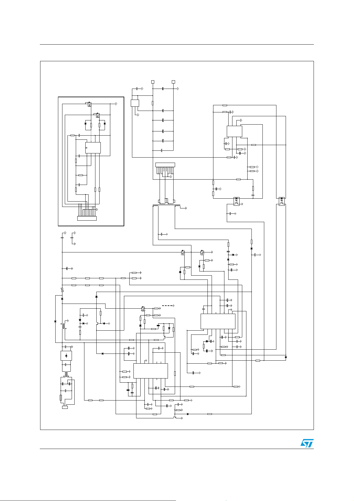
Figure 3. Electrical diagram
FASTONJ3FASTON
C38
100N
C38
100N
C37
470uF-16V
C37
470uF-16V
C50
470uF-16V
C50
470uF-16V
C49
470uF-16V
C49
470uF-16V
C30
C30
470uF-16V
470uF-16V
C29
C29
470uF-16V
470uF-16V
12345678910111213
91012138
4
R23
0R47
R23
0R47
R22
0R27
R22
0R27
C33
1NF
C33
1NF
R20
33R
R20
33R
R52
1K5
R52
1K5
R55
2K7
R55
2K7
C16
2N2
C16
2N2
10
11
NC
PWM-STOP
C22
220PF
C22
220PF
R37
220K
R37
220K
J2
FASTONJ2FASTON
R68
39K
R68
39K
C51
100N
C51
100N
R73
22R
R73
22R
6
8
5
7
VCC
GND
CV_OUT
CC_OUT
CV-
V_REF
CC+3CC-
U5
TSM1014AISTU5TSM1014AIST
4
1
2
C481NC48
1N
R72
330K
R72
330K
C32
1uF
C32
1uF
R711KR71
1K
R43
51R
R43
51R
C36
1uF - 50V
C36
1uF - 50V
R421KR42
Q4
STF8NM50NQ4STF8NM50N
213
R59
100K
R59
100K
R38
56R
R38
56R
D19
1N4148
D19
1N4148
1 2
C19
100N
C19
100N
16
15
HVG
VBOOT
CSS1DELAY2CF3RFMIN4STBY5ISEN6LINE
U2
L6599ADU2L6599AD
12
D16
D16
1N4148
1N4148
R16
4K7
R16
4K7
1M0
1M0
C18
4u7F
C18
4u7F
1K
14
OUT
C17
330PF
C17
330PF
C6
4N7C64N7
R44
6K2
R44
6K2
R77
1K0
R77
1K0
11
14
7
6
C28
22NF
C28
22NF
STF8NM50NQ3STF8NM50N
Q3
213
R58
100K
R58
100K
D18
1N4148
D18
1N4148
R25
56R
R25
56R
1 2
HS1
HEAT-SINK
HS1
HEAT-SINK
D6
1N4148D61N4148
23
R53
2K2
R53
2K2
1
Q2
BC857Q2BC857
9
HVS
R27
470R
R27
470R
8
C10
1N0
C10
1N0
R15
56K
R15
56K
C12
1uF
C12
1uF
1
32
BC847CQ9BC847C
R24
R24
C45
220NF
C45
220NF
R29
1K0
R29
1K0
R26
1M0
R26
1M0
1N
C521NC52
D12
BZV55-C43
D12
BZV55-C43
R76
R76
33K
33K
21
Q9
12
43
U3
SFH617A-2U3SFH617A-2
C41
22N
C41
22N
R41
100R
R41
100R
D11
D11
C27
C27
220PF-630V
220PF-630V
12
D10
1N4148
D10
1N4148
1 2
R39
160R
R39
160R
C25
2u2
C25
2u2
C26
C26
10uF-50V
10uF-50V
C40
100N
C40
100N
13
11
12
10
9
NC
LVG
VCC
GND
PFC-STOP
DIS
7
8
C44
470pF
C44
470pF
R36
1M8
R36
1M8
C23
C23
R32
47R
R32
47R
R31
12K
R31
12K
R60
10K
R60
10K
R64
10Meg
R64
10Meg
R70
22k
R70
22k
C471NC47
1N
R51
82K
R51
82K
R50
12K
R50
12K
R49
91K
R49
91K
R48
47K
R48
47K
C34
100N
C34
100N
R40
0R33
R40
0R33
D9
1 2
1N4148
1N4148
R30
R30
C43
C43
10N
10N
C24
220uF-50V
C24
220uF-50V
STPS1L60AD9STPS1L60A
10R
10R
4N7
4N7
R34
R34
6K2
6K2
12
43
U4
SFH617A-2U4SFH617A-2
12
D17
1N4148
D17
1N4148
J3
C42
100N
C42
100N
5
Vcc
U6
Out1GND2Vp
Q502
STL140N4LLF5
Q502
R502
R502
R501
10R
R501
10R
8
6
7
GD1
VCC
PGND
SGND1EN2DVS13DVS2
R506
330R
R506
330R
101112
13
R11
2M2
R11
2M2
R3
1M0R31M0
D21
1N4148
D21
1N4148
1 2
10uF-50VC810uF-50V
32
Q8
BC847CQ8BC847C
R1
3M3R13M3
STL140N4LLF5
10R
10R
D502
BAS316
D502
BAS316
5
GD2
4
R507
330R
R507
330R
EVLSRK2000-L-40
R13
8K2
R13
R12
2M2
R12
2M2
R8
1M0R81M0
R69
4K7
R69
4K7
D20
BZV55-B15
D20
BZV55-B15
1
D7
STPS140ZD7STPS140Z
1 2
R2
3M3R23M3
8K2
2 1
R19
R19
C39
100N
C39
100N
C15
47uF-50V
C15
47uF-50V
U1
L6563HU1L6563H
R10
27K
R10
27K
R9
62KR962K
C14
68N
C14
68N
Q501
STL140N4LLF5
Q501
STL140N4LLF5
D501
BAS316
D501
BAS316
R503
10R
R503
10R
C503
1uF
C503
1uF
U501
SRK2000
U501
SRK2000
C502
100nF
C502
100nF
R504
150k
R504
150k
R505
33k
R505
33k
C501
4nF7
C501
4nF7
RX1
0R0
RX1
0R0
123456789
JP501JP501
C20
2N2-Y1
C20
2N2-Y1
C21
2N2-Y1
C21
2N2-Y1
C9
100uF - 450VC9100uF - 450V
R17
2M2
R17
2M2
R7
1M0R71M0
R6
NTC 2R5-S237R6NTC 2R5-S237
12
D4
STTH5L06D4STTH5L06
D3
1N4005D31N4005
12
L2
1975.0004L21975.0004
D1
D1
GBU8J
GBU8J
L1
2019.0002L12019.0002
F1
FUSE T4AF1FUSE T4A
J1
MKDS 1,5/ 3-5,08J1MKDS 1,5/ 3-5,08
9 5
11 3
+
+
2 4
124
C2
2N2-Y1C22N2-Y1
123
C4
C1
C5
470N-X2C4470N-X2
470N-X2C1470N-X2
_
_
3 1
3
C3
2N2-Y1C32N2-Y1
90-264Vac
D5
C7
R5
470N - 520VC5470N - 520V
12
1N4148D51N4148
C8
12
D2
100NC7100N
1N4148D21N4148
10RR510R
12V-12.5A
4
Vm
R57
R002
R57
R002
TSC101U6TSC101
3
T1
1860.0034T11860.0034
2
R35
180K
R35
180K
R28
33K
R28
33K
Q1
STF19NM50NQ1STF19NM50N
213
R46
100K
R46
100K
R45
3R3
R45
3R3
R21
22R
R21
22R
D14
1N4148
D14
1N4148
1 2
56K
56K
16
14
15
13
12
GD
ZCD
VCC
RUN
GND
INV1COMP2MULT3CS4VFF5TBO6PFC-OK7PWM-LATCH
R18
82K
R18
82K
C13
680N
C13
680N
C11
2N2
C11
2N2
R14
51K
R14
51K
10/35 Doc ID 17595 Rev 1
Page 11
AN3233 Efficiency measurement
2 Efficiency measurement
EPA rev. 2.0 external power supply compliance verification
Tab l e 1 shows the no-load consumption and the overall efficiency, measured at the nominal
mains voltages. At 115 Vac the average efficiency is 90.6 %, while at 230 Vac it is 91.8 %.
Both values are much higher than the 87 % required by EPA rev 2.0 external power supply
(EPS) limits.
The efficiency at nominal load, 230 Vac, is 94 %, which is a very high efficiency for a double
stage converter and confirms the benefit of implemented SR.
Also at no load the board performances are superior: maximum no-load consumption at
nominal mains voltage is 200 mW; this value is significantly lower than the limit imposed by
the ENERGY STAR program which is 500 mW.
Table 1. Overall efficiency
230 V - 50 Hz 115 V - 60 Hz
Test
No load 12.10 0.00 0.00 0.20 ----------- 12.10 0.00 0.00 0.20 -----------
25 % load eff. 12.14 3.10 37.63 43.15 87.2 % 12.13 3.10 37.60 43.08 87.3 %
50 % load eff. 12.14 6.19 75.15 81.30 92.4 % 12.12 6.19 75.02 82.34 91.1 %
75 % load eff. 12.08 9.37 113.19 120.81 93.7 % 12.07 9.38 113.22 123.00 92.0 %
100 % load eff. 12.04 12.47 150.14 159.79 94.0 % 12.04 12.50 150.50 163.90 91.8 %
Average eff. 91.8 % 90.6 %
Vout
[V]
Iout
[A]
Pout
[W]
Pin
[W]
Eff.
[%]
Vou t
[V]
Iout
[A]
Pout
[W]
Pin
[W]
Eff.
[%]
Doc ID 17595 Rev 1 11/35
Page 12

Efficiency measurement AN3233
Light load operation efficiency
Measurement results are reported in Ta b l e 2 and plotted in Figure 4. As can be seen,
efficiency is better than 50 % even for very light loads such as 500 mW.
Table 2. Light load efficiency
230 V - 50 Hz 115 V - 60 Hz
Test
Vou t
[V]
Iout
[mA]
Pout
[W]
Pin
[W]
Eff.
[%]
Vout
[V]
Iout
[mA]
Pout
[W]
Pin
[W]
Eff.
0.25 W 12.12 20.84 0.253 0.581 43.5 % 12.12 20.84 0.253 0.565 44.7 %
0.5 W 12.12 41.34 0.501 0.931 53.8 % 12.12 41.34 0.501 0.912 55.0 %
1.0 W 12.12 82.65 1.002 1.553 64.5 % 12.12 82.65 1.002 1.552 64.5 %
1.5 W 12.12 123.93 1.502 2.203 68.2 % 12.12 123.93 1.502 2.211 67.9 %
2.0 W 12.12 164.93 1.999 2.797 71.5 % 12.12 164.93 1.999 2.828 70.7 %
2.5 W 12.12 206.75 2.506 3.392 73.9 % 12.12 206.75 2.506 3.439 72.9 %
3.0 W 12.11 248.00 3.003 3.979 75.5 % 12.11 248.00 3.003 4.040 74.3 %
3.5 W 12.11 288.25 3.491 4.560 76.6 % 12.11 288.25 3.491 4.644 75.2 %
4.0 W 12.11 330.06 3.997 5.155 77.5 % 12.11 330.06 3.997 5.258 76.0 %
4.5 W 12.11 372.31 4.509 5.748 78.4 % 12.11 372.31 4.509 5.874 76.8 %
5.0 W 12.11 413.34 5.006 6.327 79.1 % 12.11 413.34 5.006 6.474 77.3 %
Figure 4. Light load efficiency diagram
80%
75%
[%]
70%
65%
60%
Efficiency [%]
55%
50%
45%
40%
0.0 0.5 1.0 1.5 2.0 2.5 3.0 3.5 4.0 4.5 5.0 5.5
Pout [W]
12/35 Doc ID 17595 Rev 1
230V-50Hz
115 V-6 0Hz
Page 13

AN3233 Harmonic content measurement
3 Harmonic content measurement
The board has been tested according to the European standard EN61000-3-2 Class-D and
the Japanese standard JEITA-MITI Class-D, at both the nominal input voltage mains. As
shown in the following images, the circuit is able to reduce the harmonics well below the
limits of both regulations.
Figure 5. Compliance with EN61000-3-2 at 230 Vac – 50 Hz, full load
Measured Value
EN610003 2 ClassD Li mits
1
1
0.1
0.1
Current [A]
0.01
Harmonic
0.001
0.0001
1 3 5791113 15 17 19 21 23 25 27 29 31 33 35 37 39
Harmonic Order [n]
THD = 14.70 % - PF = 0.978
Figure 6. Compliance with JEITA-MITI at 100 Vac – 50 Hz, full load
Measured Value
JEITAMITI Class D Limits
1
1
[A]
0.1
0.1
Current
0.01
Harmonic
0.001
0.0001
1 3 5791113 15 17 19 21 23 25 27 29 31 33 35 37 39
Harmonic Order [n]
THD = 5.20 % - PF = 0.995
On the bottom side of the diagrams the total harmonic distortion (THD) and power factor
(PF) have been measured too. The values in all conditions give a clear idea regarding the
correct functioning of the PFC.
Doc ID 17595 Rev 1 13/35
Page 14

Functional check AN3233
4 Functional check
Steady-state operation
In Figure 7 some waveforms relevant to the resonant stage during steady-state operation
are given. The selected switching frequency is about 120 kHz, in order to have a good trade
off between transformer losses and dimensions. The converter operates slightly above the
resonance frequency.
Figure 8 shows the key signals of SRK2000: each rectifier MOSFET is switched on and off
according to its drain-source voltage which, during conduction time, is the voltage image of
the current flowing through the MOSFET.
Figure 7. Resonant stage waveforms
CH1: HB voltage CH2: CF pin voltage CH1: GD1 pin voltage CH2: DVS1 pin
at 115 V – 60 Hz – full load
CH4: Res. tank current CH3: GD2 pin voltage CH4: DVS2 pin
Figure 8. SRK2000 key signals
at 115 V – 60 Hz – full load
14/35 Doc ID 17595 Rev 1
Page 15

AN3233 Functional check
Zero voltage switching
Figure 9 and 10 show details of ZVS operation. Both MOSFETs turn on when current is
flowing through their body diodes and drain-source voltage is zero.
Figure 9. High-side MOSFET ZV turn-on
CH1: HB voltage CH2: HVG pin voltage CH1: HB voltage CH2: HVG pin voltage
CH3: LVG pin voltage CH3: LVG pin voltage
at 115 V – 60 Hz – full load
Figure 10. Low-side MOSFET ZV turn-on
at 115 V – 60 Hz – full load
Startup and shutdown
Figure 11 and 12 show the start-up and shut-down sequence of the two converter stages:
The PFC starts first and the LLC only starts after the PFC achieves regulation. In the same
way the PFC stops first and the LLC shuts down as its input voltage falls below the allowed
voltage.
Figure 11. Converter startup
CH1: Half-bridge node CH2: PFC drain CH1: Half-bridge node CH2: PFC drain
CH3: Output voltage CH4: LINE pin CH3: Output voltage CH4: LINE pin
at 115 Vac full load
Figure 12. Converter shutdown
at 115 Vac full load
Figure 13 and 14 again show startup and shutdown but highlighting the current flowing
through the resonant tank.
Doc ID 17595 Rev 1 15/35
Page 16

Functional check AN3233
In Figure 13 it can be noted that the resonant current at turn-on has some oscillations due to
the charging of the resonant elements. However, current zero-crossing always lags the HB
commutations and, consequently, MOSFETs are soft switched.
Figure 14 shows the resonance current at shutdown. Due to input voltage dip, the LLC stage
operates below resonance, but current still lags the HB voltage.
Avoiding hard switching also during transitions like startup and shutdown is a must for a
reliable design, because some hard switching commutations could also damage the
converter.
Figure 13. Startup resonant current Figure 14. Shutdown resonant current
CH1: Half-bridge CH3 C6 voltage CH1: Half-bridge
CH4: Res. tank current CH4: Res. tank current
No-load operation
In Figure 15 and 16, some burst mode waveforms are captured. As seen, both L6599A and
L6563H operate in burst mode. In
are synchronized.
Figure 15. No-load operation Figure 16. No-load operation – detail
CH1: LVG pin CH2: PFC gate CH1: Half-bridge CH2: PFC Drain
CH3: Output voltage CH4: STBY pin CH3: PFC-STOP pin CH4: STBY pin
Figure 16, it is possible to see that PFC and LLC bursts
16/35 Doc ID 17595 Rev 1
Page 17

AN3233 Functional check
In Figure 17 and 18 the transitions from full load to no load and vice versa have been
checked. As seen in the images, both transitions are clean and there isn’t any output voltage
dip.
Figure 17. Transition full load to no load
CH1: LVG pin CH2: PFC gate CH1: LVG pin CH2: PFC gate
CH3: Output voltage CH4: Output current CH3: Output voltage CH4: Output current
at 115 Vac – 60 Hz
Figure 18. Transition no load to full load
at 115 Vac – 60 Hz
Overcurrent and short-circuit protection
The L6599A is equipped with a current sensing input (pin 6, ISEN) and a dedicated
overcurrent management system. The current flowing in the resonant tank is detected and
the signal is fed into the ISEN pin. It is internally connected to a first comparator, referenced
to 0.8 V, and to a second comparator referenced to 1.5 V. If the voltage externally applied to
the pin exceeds 0.8 V, the first comparator is tripped causing an internal switch to be turned
on and the soft-start capacitor CSS to be discharged.
Under output short-circuit, this operation results in an almost constant peak primary current.
With the L6599A, the board designer can externally program the maximum time that the
converter is allowed to run overloaded or under short-circuit conditions. Overloads or shortcircuits lasting less than the set time do not cause any other action, therefore providing the
system with immunity to short duration phenomena. If, instead, the overload condition
continues, a protection procedure is activated that shuts down the L6599A and, in case of
continuous overload/short-circuit, results in continuous intermittent operation with a user
defined duty cycle. This function is realized with the DELAY pin (pin 2), by means of a
capacitor C45 and the parallel resistor R24 connected to ground. As the voltage on the
ISEN pin exceeds 0.8 V, the first OCP comparator, in addition to discharging CSS, turns on
an internal 150 µA current generator that, via the DELAY pin, charges C45. As the voltage
on C45 is 3.5 V, the L6599A stops switching and the PFC_STOP pin is pulled low. Also the
internal generator is turned off, so that C45 is now slowly discharged by R24. The IC
restarts when the voltage on C45 is less than 0.3 V. Additionally, if the voltage on the ISEN
pin reaches 1.5 V for any reason (e.g. transformer saturation), the second comparator is
triggered, the L6599A shuts down and the operation is resumed after an off-on cycle.
Figure 19 shows intermittent operations caused by an output short-circuit: average output
current is limited, preventing the converter from overheating and consequent failure.
Doc ID 17595 Rev 1 17/35
Page 18

Functional check AN3233
Figure 19. Short-circuit at full load and 115 Vac – 60 Hz
CH1: LVG pin CH2: Output voltage
CH3: DELAY pin CH4: Output current
18/35 Doc ID 17595 Rev 1
Page 19

AN3233 Thermal map
5 Thermal map
In order to check the design reliability, a thermal mapping by means of an IR camera was
done. In
nominal input voltage, are shown. Some pointers, visible in the images, have been placed
across key components or components showing high temperature. The ambient
temperature during both measurements was 27 °C.
Figure 20. Thermal map at 115 Vac – 60 Hz - full load
Figure 20 and 21 the thermal measurements of the board, component side, at
Figure 21. Thermal map at 230 Vac – 50 Hz - full load
Table 3. Thermal maps reference points
Point Reference Description
A D1 Bridge rectifier
B L1 EMI filtering inductor
C L2 PFC inductor
D Q8 ICs supply regulator
E D4 PFC output diode
F R6 Inrush limiting NTC resistor
G Q4 Resonant low side MOSFET
H T1 Resonant power transformer
Doc ID 17595 Rev 1 19/35
Page 20

Thermal map AN3233
To directly check the efficiency of the SR stage, a thermal map of the SR daughterboard has
also been taken. As seen, the temperature of both rectifier MOSFETs is below 70 °C,
confirming that heatsinking is not required and confirming that the SR solution implemented
allows a significant secondary side board dimension squeezing.
Figure 22. Thermal map SR daughterboard - full load
Table 4. Daughterboard thermal map reference points
Point Reference Description
SP1 Q501 SR MOSFET
SP2 Q502 SR MOSFET
20/35 Doc ID 17595 Rev 1
Page 21

AN3233 Conducted emission pre-compliance test
6 Conducted emission pre-compliance test
Figure 23 and 24 represent the average measurement of the conducted emission at full load
and nominal mains voltages. The limit indicated in red on the diagrams is relevant to
average measurements and is the EN55022 Class-B one, which has more severe limits
compared to Class-A, dedicated to IT technology equipment. As can be seen, in all test
conditions the measurements are significantly below the limits.
Figure 23. CE average measurement at 115 Vac and full load
Figure 24. CE average measurement at 230 Vac and full load
Doc ID 17595 Rev 1 21/35
Page 22

7 Bill of material
Table 5. EVL150W-ADP-SR demonstration board: motherboard bill of materials
AN3233 Bill of material
Doc ID 17595 Rev 1 22/35
Des.
C1 470N X2 - film cap - B32922C3474K EPCOS 9.0 × 18.0 p15 mm
C2 2N2 Y1 safety cap. DE1E3KX222M MURATA p10 mm
C3 2N2 Y1 safety cap. DE1E3KX222M MURATA p10 mm
C4 470N X2 - film cap - B32922C3474K EPCOS 9.0 × 18.0 p15 mm
C5 470N 520 V - film cap - B32673Z5474K EPCOS 7.0 x 26.5 p22.5 mm
C6 4N7 50 V cercap - general purpose AVX 0805
C7 100N 100 V cercap - general purpose AVX PTH
C8 10 uF - 50 V Aluminium elcap - YXF series - 105 °C RUBYCON DIA 5.0 x 11 p2 mm
C9 100 uF - 450 V Aluminium elcap - UPZ2W101MHD NICHICON DIA 18 x 32 mm
C10 1N0 50 V cercap - general purpose AVX 0805
C11 2N2 50 V cercap - general purpose AVX 0805
C12 1 uF 25 V cercap - general purpose AVX 0805
C13 680N 25 V cercap - general purpose AVX 1206
C14 68N 50 V cercap - general purpose AVX 0805
C15 47 uF - 50 V Aluminium elcap - YXF series - 105 °C RUBYCON DIA 6.3 x 11p2.5 mm
C16 2N2 50 V cercap - general purpose AVX 1206
C17 330PF 50 V - 5 % - C0G - cercap AVX 0805
Part type/
part value
Description Supplier Case
C18 4u7F 25 V cercap - general purpose MURATA 1206
C19 100N 50 V cercap - general purpose AVX 1206
C20 2N2 Y1 safety cap. DE1E3KX222M MURATA p10 mm
C21 2N2 Y1 safety cap. DE1E3KX222M MURATA p10 mm
Page 23

23/35 Doc ID 17595 Rev 1
Table 5. EVL150W-ADP-SR demonstration board: motherboard bill of materials (continued)
Bill of material AN3233
Des.
C22 220PF 50 V cercap - general purpose AVX 0805
C23 10N 50 V cercap - general purpose AVX 0805
C24 220 uF - 50 V Aluminium elcap - YXF series - 105 °C RUBYCON DIA10 x 16 p5 mm
C25 2u2 50 V cercap - general purpose AVX 0805
C26 10 uF - 50 V Aluminium elcap - YXF series - 105 °C RUBYCON DIA 5.0 x 11 p2 mm
C27 220 pF - 630 V 630 V cercap - GRM31A7U2J220JW31 MURATA 1206
C28 22NF 1 KV - film cap - B32652A223K EPCOS 5.0 x 18.0 p15 mm
C29 470 uF - 16 V 16 V aluminium solid capacitor SANYO DIA 10 X 13 p5 mm
C30 470 uF - 16 V 16 V aluminium solid capacitor SANYO DIA 10 x 13 p5 mm
C32 1 uF 50 V cercap - general purpose AVX 0805
C33 1NF 50 V cercap - general purpose AVX 0805
C34 100N 50 V cercap - general purpose AVX 0805
C36 1 uF - 350 V 50 V cercap - general purpose AVX 1206
C37 470 uF - 16 V 16 V aluminium solid capacitor SANYO DIA 10 x 13 p5 mm
C38 100N 50 V cercap - general purpose AVX 0805
C39 100N 50 V cercap - general purpose AVX 0805
Part type/
part value
Description Supplier Case
C40 100N 50 V cercap - general purpose AVX 1206
C41 22N 50 V cercap - general purpose AVX 0805
C42 100N 50 V cercap - general purpose AVX 0805
C43 4N7 50 V cercap - general purpose AVX 0805
C44 3N3 50 V cercap - general purpose AVX 0805
C45 220NF 25 V cercap - general purpose AVX 0805
C47 1N 50 V cercap - general purpose AVX 0805
C48 1N 50 V cercap - general purpose AVX 0805
Page 24

Table 5. EVL150W-ADP-SR demonstration board: motherboard bill of materials (continued)
AN3233 Bill of material
Doc ID 17595 Rev 1 24/35
Des.
C49 470 uF 16 V aluminium solid capacitor SANYO DIA 10 x 13 p5 mm
C50 470 uF 16 V aluminium solid capacitor SANYO DIA 10 x 13 p5 mm
C51 100N 50 V cercap - general purpose AVX 0805
C52 1N 25 V cercap - general purpose AVX 0805
D1 GBU8J Single phase bridge rectifier VISHAY STYLE GBU
D2 LL4148 High speed signal diode VISHAY Minimelf SOD-80
D3 1N4005 General purpose rectifier VISHAY DO-41 DO - 41
D4 STTH5L06 Ultrafast high voltage rectifier STMicroelectronics DO-201
D5 LL4148 High speed signal diode VISHAY Minimelf SOD-80
D6 LL4148 High speed signal diode VISHAY Minimelf SOD-80
D7 STPS140Z Power Schottky rectifier STMicroelectronics SOD-123
D9 STPS1L60A Power schottky diode STMicroelectronics SMA
D10 LL4148 High speed signal diode VISHAY Minimelf SOD-80
D11 LL4148 High speed signal diode VISHAY Minimelf SOD-80
D12 BZV55-C43 Zener diode VISHAY Minimelf SOD-80
D14 LL4148 High speed signal diode VISHAY Minimelf SOD-80
Part type/
part value
Description Supplier Case
D16 LL4148 High speed signal diode VISHAY Minimelf SOD-80
D17 LL4148 High speed signal diode VISHAY Minimelf SOD-80
D18 LL4148 High speed signal diode VISHAY Minimelf SOD-80
D19 LL4148 High speed signal diode VISHAY Minimelf SOD-80
D20 BZV55-B15 Zener diode VISHAY Minimelf SOD-80
D21 LL4148 High speed signal diode VISHAY Minimelf SOD-80
F1 FUSE T4A Fuse 4A - time lag - 3921400 LITTLEFUSE 8.5x4 p.5.08 mm
HS1 HEAT-SINK Heat sink for D1, Q1, Q3, Q4 DWG
Page 25

25/35 Doc ID 17595 Rev 1
Table 5. EVL150W-ADP-SR demonstration board: motherboard bill of materials (continued)
Bill of material AN3233
Des.
J1 MKDS 1,5/ 3-5,08 PCB term. block, screw conn., pitch 5 mm - 3 W PHOENIX CONTACT DWG
J2 FASTON Faston - connector DWG
J3 FASTON Faston - connector DWG
L1 2019.0002 Common mode choke - EMI filter MAGNETICA DWG
L2 1975.0004 PFC inductor - 0.31 mH - PQ26/25 MAGNETICA DWG
Q1 STF19NM50N N-channel power MOSFET STMicroelectronics TO-220FP
Q2 BC857 PNP small signal BJT VISHAY SOT-23
Q3 STF8NM50N N-channel power MOSFET STMicroelectronics TO-220FP
Q4 STF8NM50N N-channel power MOSFET STMicroelectronics TO-220FP
Q8 BC847C NPN small signal BJT VISHAY SOT-23
Q9 BC847C NPN small signal BJT VISHAY SOT-23
R1 3M3 SMD film res - 1/4 W - 5 % - 250 ppm/°C VISHAY 1206
R2 3M3 SMD film res - 1/4 W - 5 % - 250 ppm/°C VISHAY 1206
R3 1M0 SMD film res - 1/4 W - 1 % - 100 ppm/°C VISHAY 1206
R5 10R SMD film res - 1/4 W - 5 % - 250 ppm/°C VISHAY 1206
R6 NTC 2R5-S237 NTC resistor P/N B57237S0259M000 EPCOS DWG
Part type/
part value
Description Supplier Case
R7 1M0 SMD film res - 1/4 W - 1 % - 100 ppm/°C VISHAY 1206
R8 1M0 SMD film res - 1/4 W - 1 % - 100 ppm/°C VISHAY 1206
R9 62K SMD film res - 1/8 W - 1 % - 100 ppm/°C VISHAY 0805
R10 27K SMD film res - 1/8 W - 1 % - 100 ppm/°C VISHAY 0805
R11 2M2 SMD film res - 1/4 W - 1 % - 100 ppm/°C VISHAY 1206
R12 2M2 SMD film res - 1/4 W - 1 % - 100 ppm/°C VISHAY 1206
R13 8K2 SMD film res - 1/4 W - 1 % - 100 ppm/°C VISHAY 1206
R14 51K SMD film res - 1/8 W - 5 % - 250 ppm/°C VISHAY 0805
Page 26

Table 5. EVL150W-ADP-SR demonstration board: motherboard bill of materials (continued)
AN3233 Bill of material
Doc ID 17595 Rev 1 26/35
Des.
R15 56K SMD film res - 1/4 W - 1 % - 100 ppm/°C VISHAY 1206
R16 4K7 SMD film res - 1/8 W - 5 % - 250 ppm/°C VISHAY 0805
R17 2M2 SMD film res - 1/4 W - 1 % - 100 ppm/°C VISHAY 1206
R18 82K SMD film res - 1/8 W - 5 % - 250 ppm/°C VISHAY 0805
R19 56K SMD film res - 1/8 W - 5 % - 250 ppm/°C VISHAY 0805
R20 33R SMD film res - 1/8 W - 5 % - 250 ppm/°C VISHAY 0805
R21 22R SMD film res - 1/8 W - 5 % - 250 ppm/°C VISHAY 0805
R22 0R27 SFR25 axial stand. film res - 0.4 W - 5 % - 250 ppm/°C VISHAY PTH
R23 0R47 SFR25 axial stand. film res - 0.4 W - 5 % - 250 ppm/°C VISHAY PTH
R24 1M0 SMD film res - 1/8 W - 5 % - 250 ppm/°C VISHAY 0805
R25 56R SMD film res - 1/8 W - 5 % - 250 ppm/°C VISHAY 0805
R26 1M0 SMD film res - 1/8 W - 1 % - 100 ppm/°C VISHAY 0805
R27 470R SMD film res - 1/4 W - 5 % - 250 ppm/°C VISHAY 1206
R28 33K SMD film res - 1/8 W - 1 % - 100 ppm/°C VISHAY 0805
R29 1K0 SMD film res - 1/4 W - 5 % - 250 ppm/°C VISHAY 1206
R30 10R SMD film res - 1/8 W - 5 % - 250 ppm/°C VISHAY 0805
Part type/
part value
Description Supplier Case
R31 12K SMD film res - 1/8 W - 1 % - 100 ppm/°C VISHAY 0805
R32 47R SMD film res - 1/8 W - 5 % - 250 ppm/°C VISHAY 0805
R34 27K SMD film res - 1/8 W - 5 % - 250 ppm/°C VISHAY 0805
R35 180K SMD film res - 1/8 W - 1 % - 100 ppm/°C VISHAY 0805
R36 1M8 SMD film res - 1/8 W - 5 % - 250 ppm/°C VISHAY 0805
R37 220K SMD film res - 1/4 W - 5 % - 250 ppm/°C VISHAY 1206
R38 56R SMD film res - 1/8 W - 5 % - 250 ppm/°C VISHAY 0805
R39 160R SMD film res - 1/8 W - 5 % - 250 ppm/°C VISHAY 0805
Page 27

27/35 Doc ID 17595 Rev 1
Table 5. EVL150W-ADP-SR demonstration board: motherboard bill of materials (continued)
Bill of material AN3233
Des.
R40 R33 SMD film res - 1/4 W - 5 % - 250 ppm/°C VISHAY 1206
R41 100R SFR25 axial stand. film res - 0.4 W - 5 % - 250 ppm/°C VISHAY PTH
R42 1K SMD film res - 1/8 W - 5 % - 250 ppm/°C VISHAY 0805
R43 51R SMD film res - 1/8 W - 5 % - 250 ppm/°C VISHAY 0805
R44 6K2 SMD film res - 1/4 W - 5 % - 250 ppm/°C VISHAY 1206
R45 3R3 SMD film res - 1/8 W - 5 % - 250 ppm/°C VISHAY 0805
R46 100K SMD film res - 1/8 W - 5 % - 250 ppm/°C VISHAY 0805
R48 47K SMD film res - 1/8 W - 5 % - 250 ppm/°C VISHAY 0805
R49 91K SMD film res - 1/4 W - 1 % - 100 ppm/°C VISHAY 1206
R50 12K SMD film res - 1/8 W - 1 % - 100 ppm/°C VISHAY 0805
R51 82K SMD film res - 1/8 W - 1 % - 100 ppm/°C VISHAY 0805
R52 1K5 SMD film res - 1/8 W - 1 % - 100 ppm/°C VISHAY 0805
R53 2K2 SMD film res - 1/8 W - 1 % - 100 ppm/°C VISHAY 0805
R54 0R0 SMD film res - 1/8 W - 5 % - 250 ppm/°C VISHAY 0805
R55 2K7 SMD film res - 1/8 W - 1 % - 100 ppm/°C VISHAY 0805
R57 R002 SMD shunt resistor - RL3264-9V-R002-FNH-11 CYNTEC 2512
Part type/
part value
Description Supplier Case
R58 100K SMD film res - 1/8 W - 5 % - 250 ppm/°C VISHAY 0805
R59 100K SMD film res - 1/8 W - 5 % - 250 ppm/°C VISHAY 0805
R60 10K SMD film res - 1/8 W - 5 % - 250 ppm/°C VISHAY 0805
R63 0R0 SMD film res - 1/8 W - 5 % - 250 ppm/°C VISHAY 0805
R64 10Meg SMD film res - 1/8 W - 5 % - 250 ppm/°C VISHAY 0805
R68 39K SMD film res - 1/8 W - 1 % - 100 ppm/°C VISHAY 0805
R69 4K7 SMD film res - 1/8 W - 5 % - 250 ppm/°C VISHAY 0805
R70 22k SMD film res - 1/8 W - 1 % - 100 ppm/°C VISHAY 0805
Page 28

Table 5. EVL150W-ADP-SR demonstration board: motherboard bill of materials (continued)
AN3233 Bill of material
Doc ID 17595 Rev 1 28/35
Des.
R71 1K SMD film res - 1/4 W - 5 % - 250 ppm/°C VISHAY 1206
R72 330K SMD film res - 1/8 W - 1 % - 100 ppm/°C VISHAY 0805
R73 22R SMD film res - 1/8 W - 5 % - 250 ppm/°C VISHAY 0805
R75 0R0 SMD film res - 1/8 W - 5 % - 250 ppm/°C VISHAY 0805
R76 33K SMD film res - 1/8 W - 5 % - 250 ppm/°C VISHAY 0805
R77 1K0 SMD film res - 1/8 W - 5 % - 250 ppm/°C VISHAY 0805
T1 1860.0034 Resonant power transformer MAGNETICA ETD34
U1 L6563H High voltage start-up TM PFC controller STMicroelectronics SO-16
U2 L6599AD Improved HV resonant controller STMicroelectronics SO-16
U3 SFH617A-2 Optocoupler INFINEON DIP-4 - 10.16 mm
U4 SFH617A-2 Optocoupler INFINEON DIP-4 - 10.16 mm
U5 TSM1014AIST Low consumption CV/CC controller STMicroelectronics MINI SO-8
U6 TSC101C High side current sense amplifier STMicroelectronics SOT23-5
Part type/
part value
Description Supplier Case
Page 29

29/35 Doc ID 17595 Rev 1
Bill of material AN3233
Table 6. EVL150W-ADP-SR evaluation board: daughter board bill of material
Des.
C501 4nF7 50 V cercap - general purpose VISHAY 0805
C502 100 nF 50 V cercap - general purpose VISHAY 0805
C503 1 uF 50 V cercap - general purpose VISHAY 0805
D501 BAS316 Fast switching signal diode STMicroelectronics SOD-123
D502 BAS316 Fast switching signal diode STMicroelectronics SOD-123
JP501 HEADER 13 13-pin connector
Q501 STL140N4LLF5 N-channel power MOSFET STMicroelectronics POWER FLAT
Q502 STL140N4LLF5 N-channel power MOSFET STMicroelectronics POWER FLAT
R501 10R SMD standard film res - 1/8 W - 5 % - 250 ppm/°C VISHAY 0805
R502 10R SMD standard film res - 1/8 W - 5 % - 250 ppm/°C VISHAY 0805
R503 10R SMD standard film res - 1/8 W - 5 % - 250 ppm/°C VISHAY 0805
R504 150k SMD standard film res - 1/8 W - 1 % - 100 ppm/°C VISHAY 0805
R505 33k SMD standard film res - 1/8 W - 1 % - 100 ppm/°C VISHAY 0805
R506 330R SMD standard film res - 1/8 W - 5 % - 250 ppm/°C VISHAY 0805
R507 330R SMD standard film res - 1/8 W - 5 % - 250 ppm/°C VISHAY 0805
RX1 0R0 SMD standard film res - 1/8 W - 5 % - 250 ppm/°C VISHAY 0805
U501 SRK2000 SR smart driver for LLC resonant converter STMicroelectronics SO8
Part type/
part value
Description Supplier Case
Page 30

PFC coil specification AN3233
8 PFC coil specification
General description and characteristics
● Application type: consumer, home appliance
● Transformer type: open
● Coil former: vertical type, 6+6 pins
● Max. temp. rise: 45 ºC
● Max. operating ambient temperature: 60 ºC
● Mains insulation: n.a.
● Unit finishing: varnished.
Electrical characteristics
● Converter topology: boost, transition mode
● Core type: PQ26/25-PC44 or equivalent
● Min. operating frequency: 40 kHz
● Typical operating frequency: 120 kHz
● Primary inductance: 310 µH±10 % at 1 kHz-0.25 V
Peak current: 5.6 Apk.
●
(a)
Electrical diagram and winding characteristics
Figure 25. PFC coil electrical diagram
5
9
Table 7. PFC coil winding data
Pins Windings RMS current Number of turns Wire type
11 - 3 AUX 0.05 A
5 - 9 PRIMARY 2.3 A
RMS
RMS
5 φ 0.28 mm – G2
50 50xφ 0.1 mm – G1
11
3
a. Measured between pins #5 and #9
30/35 Doc ID 17595 Rev 1
Page 31

AN3233 PFC coil specification
Mechanical aspects and pin numbering
● Maximum height from PCB: 30 mm
● Coil former type: vertical, 6+6 pins (Pins 1, 2, 4, 6, 7, 10, 12 are removed)
● Pin distance: 3.81 mm
● Row distance: 25.4 mm
● External copper shield: not insulated, wound around the ferrite core and including the
coil former. Height is 8 mm. Connected to pin #3 by a soldered solid wire.
Figure 26. PFC coil mechanical aspect
30 MAX
11
3
11
11.43
3.81
3.81
9
8
25.40
28 MAX
30 MAX
3 5 9
3
22.86
5
11.43
3.81
IMENSIONS IN MILLIMETERS, DRAWING NOT IN SCALE
Manufacturer
● Magnetica - Italy
● Inductor P/N: 1975.0004
Doc ID 17595 Rev 1 31/35
BOTTOM VIEW (PIN SIDE)
∅ 0.9 (X5)
R
ECOMMENDED
PCB
HOLE
∅1.3
Page 32

Transformer specifications AN3233
9 Transformer specifications
General description and characteristics
● Application type: consumer, home appliance
● Transformer type: open
● Coil former: horizontal type, 7+7 pins, two slots
● Max. temp. rise: 45 ºC
● Max. operating ambient temperature: 60 ºC
● Mains insulation: Acc. With EN60065.
Electrical characteristics
● Converter topology: half bridge, resonant
● Core type: ETD34-PC44 or equivalent
● Min. operating frequency: 60 kHz
● Typical operating frequency: 100 kHz
● Primary inductance: 800 µH ±10 % at 1 kHz-0.25 V
Leakage inductance: 100 µH ±10 % at 100 kHz-0.25 V
●
(b)
(c)
.
Electrical diagram and winding characteristics
Figure 27. Transformer electrical diagram
2
4
6
7
8
9
10
11
12
13
14
b. Measured between pins 2-4
c. Measured between pins 2-4 with only half secondary winding shorted at time
32/35 Doc ID 17595 Rev 1
Page 33

AN3233 Transformer specifications
Table 8. Transformer winding data
Pins Winding RMS current Number of turns Wire type
2 - 4 PRIMARY 1.2 A
8 - 11 SEC-1A
9 -10 SEC-1B
10 - 13 SEC-2A
12 - 14 SEC-2B
6 - 7 AUX
(2)
4
4
(1)
4
5 A
5 A
5 A
5 A
0.05 A
RMS
RMS
RMS
RMS
RMS
RMS
34 30 x φ 0.1 mm – G1
290 x φ 0.1 mm – G1
290 x φ 0.1 mm – G1
290 x φ 0.1 mm – G1
290 x φ 0.1 mm – G1
3 φ 0.28 mm– G2
1. Secondary windings A and B are in parallel
2. Aux winding is wound on top of primary winding
Mechanical aspect and pin numbering
● Maximum height from PCB: 30 mm
● Coil former type: horizontal, 7+7 pins (pins #3 and #5 are removed)
● Pin distance: 5.08 mm
● Row distance: 25.4 mm.
Figure 28. Transformer overall drawing
39
MAX
30
MAX
QUOTES IN MILLIMETERS, DRAWING NOT IN SCALE
Manufacturer
● Magnetica - Italy
● Transformer P/N: 1860.0034
MISSING PIN 3 AND
AS
PCB
REFERENCE
5.08
5
PIN SIDE VIEW
1 2 4 6 7
14 13 12 11 10 9 8
39
25.4
LABEL
MAX
3
MIN
Ø1.1 (x12) / PCB hole Ø1.6
Doc ID 17595 Rev 1 33/35
Page 34

Revision history AN3233
10 Revision history
Table 9. Document revision history
Date Revision Changes
13-Jan-2011 1 Initial release
34/35 Doc ID 17595 Rev 1
Page 35

AN3233
Please Read Carefully:
Information in this document is provided solely in connection with ST products. STMicroelectronics NV and its subsidiaries (“ST”) reserve the
right to make changes, corrections, modifications or improvements, to this document, and the products and services described herein at any
time, without notice.
All ST products are sold pursuant to ST’s terms and conditions of sale.
Purchasers are solely responsible for the choice, selection and use of the ST products and services described herein, and ST assumes no
liability whatsoever relating to the choice, selection or use of the ST products and services described herein.
No license, express or implied, by estoppel or otherwise, to any intellectual property rights is granted under this document. If any part of this
document refers to any third party products or services it shall not be deemed a license grant by ST for the use of such third party products
or services, or any intellectual property contained therein or considered as a warranty covering the use in any manner whatsoever of such
third party products or services or any intellectual property contained therein.
UNLESS OTHERWISE SET FORTH IN ST’S TERMS AND CONDITIONS OF SALE ST DISCLAIMS ANY EXPRESS OR IMPLIED
WARRANTY WITH RESPECT TO THE USE AND/OR SALE OF ST PRODUCTS INCLUDING WITHOUT LIMITATION IMPLIED
WARRANTIES OF MERCHANTABILITY, FITNESS FOR A PARTICULAR PURPOSE (AND THEIR EQUIVALENTS UNDER THE LAWS
OF ANY JURISDICTION), OR INFRINGEMENT OF ANY PATENT, COPYRIGHT OR OTHER INTELLECTUAL PROPERTY RIGHT.
UNLESS EXPRESSLY APPROVED IN WRITING BY AN AUTHORIZED ST REPRESENTATIVE, ST PRODUCTS ARE NOT
RECOMMENDED, AUTHORIZED OR WARRANTED FOR USE IN MILITARY, AIR CRAFT, SPACE, LIFE SAVING, OR LIFE SUSTAINING
APPLICATIONS, NOR IN PRODUCTS OR SYSTEMS WHERE FAILURE OR MALFUNCTION MAY RESULT IN PERSONAL INJURY,
DEATH, OR SEVERE PROPERTY OR ENVIRONMENTAL DAMAGE. ST PRODUCTS WHICH ARE NOT SPECIFIED AS "AUTOMOTIVE
GRADE" MAY ONLY BE USED IN AUTOMOTIVE APPLICATIONS AT USER’S OWN RISK.
Resale of ST products with provisions different from the statements and/or technical features set forth in this document shall immediately void
any warranty granted by ST for the ST product or service described herein and shall not create or extend in any manner whatsoever, any
liability of ST.
ST and the ST logo are trademarks or registered trademarks of ST in various countries.
Information in this document supersedes and replaces all information previously supplied.
The ST logo is a registered trademark of STMicroelectronics. All other names are the property of their respective owners.
© 2011 STMicroelectronics - All rights reserved
STMicroelectronics group of companies
Australia - Belgium - Brazil - Canada - China - Czech Republic - Finland - France - Germany - Hong Kong - India - Israel - Italy - Japan -
Malaysia - Malta - Morocco - Philippines - Singapore - Spain - Sweden - Switzerland - United Kingdom - United States of America
www.st.com
Doc ID 17595 Rev 1 35/35
 Loading...