

Page 1

AN3060
Application note
Applications guide for serial real-time clocks (RTCs)
By Doug Sams
Introduction
ST’s family of serial real-time clocks (RTCs) has been very popular with users. Over the
years, many topics associated with these devices have been addressed by the applications
groups supporting them. This document is a compilation of some of the most common
issues addessed ranging from layout considerations for crystals to proper software access
upon power-up. Readers will find this helpful in understanding some of the subtleties of
RTCs and what it takes to keep them running reliably.
July 2012 Doc ID 16253 Rev 2 1/23
www.st.com
Page 2

Contents AN3060
Contents
1 Layout considerations . . . . . . . . . . . . . . . . . . . . . . . . . . . . . . . . . . . . . . . 5
1.1 What are some basic layout considerations for the RTC crystal? . . . . . . . 5
2 Oscillator circuit . . . . . . . . . . . . . . . . . . . . . . . . . . . . . . . . . . . . . . . . . . . . 6
2.1 Besides the crystal, what other components do I need to add to make my
RTC oscillator work correctly? . . . . . . . . . . . . . . . . . . . . . . . . . . . . . . . . . . 6
3 Undershoot . . . . . . . . . . . . . . . . . . . . . . . . . . . . . . . . . . . . . . . . . . . . . . . . 8
3.1 Can undershoot affect operation of my real-time clock? How? What can be
done to guard against it? . . . . . . . . . . . . . . . . . . . . . . . . . . . . . . . . . . . . . . 8
4 Switchover voltage . . . . . . . . . . . . . . . . . . . . . . . . . . . . . . . . . . . . . . . . . . 9
4.1 Does the switchover voltage depend on the battery level? Or is it always a
fixed value? What is the maximum battery voltage for an RTC? . . . . . . . . 9
5 Oscillator fail detect . . . . . . . . . . . . . . . . . . . . . . . . . . . . . . . . . . . . . . . . 12
5.1 What is the OF bit? How does it work? . . . . . . . . . . . . . . . . . . . . . . . . . . 12
6 Battery low detect . . . . . . . . . . . . . . . . . . . . . . . . . . . . . . . . . . . . . . . . . . 13
6.1 How does the battery low bit work? Can it detect a missing battery? . . . 13
7 Halt (HT) bit . . . . . . . . . . . . . . . . . . . . . . . . . . . . . . . . . . . . . . . . . . . . . . . 15
7.1 What does the halt bit (HT) do? How do I use it? . . . . . . . . . . . . . . . . . . 15
8 RTC initialization . . . . . . . . . . . . . . . . . . . . . . . . . . . . . . . . . . . . . . . . . . . 18
8.1 What is the best sequence for accessing the RTC at first power-up? On
subsequent power-ups? . . . . . . . . . . . . . . . . . . . . . . . . . . . . . . . . . . . . . . 18
9 Revision history . . . . . . . . . . . . . . . . . . . . . . . . . . . . . . . . . . . . . . . . . . . 22
2/23 Doc ID 16253 Rev 2
Page 3

AN3060 List of tables
List of tables
Table 1. Summary of deselect and switchover thresholds . . . . . . . . . . . . . . . . . . . . . . . . . . . . . . . . 10
Table 2. M41T81S register map . . . . . . . . . . . . . . . . . . . . . . . . . . . . . . . . . . . . . . . . . . . . . . . . . . . . 13
Table 3. M41ST85W register map . . . . . . . . . . . . . . . . . . . . . . . . . . . . . . . . . . . . . . . . . . . . . . . . . . 15
Table 4. Document revision history . . . . . . . . . . . . . . . . . . . . . . . . . . . . . . . . . . . . . . . . . . . . . . . . . 22
Doc ID 16253 Rev 2 3/23
Page 4

List of figures AN3060
List of figures
Figure 1. Layout considerations . . . . . . . . . . . . . . . . . . . . . . . . . . . . . . . . . . . . . . . . . . . . . . . . . . . . . . 5
Figure 2. Built-in load capacitors . . . . . . . . . . . . . . . . . . . . . . . . . . . . . . . . . . . . . . . . . . . . . . . . . . . . . 6
Figure 3. Typical parasitic diode . . . . . . . . . . . . . . . . . . . . . . . . . . . . . . . . . . . . . . . . . . . . . . . . . . . . . 8
Figure 4. Undershoot protection . . . . . . . . . . . . . . . . . . . . . . . . . . . . . . . . . . . . . . . . . . . . . . . . . . . . . 8
Figure 5. Typical switchover circuits . . . . . . . . . . . . . . . . . . . . . . . . . . . . . . . . . . . . . . . . . . . . . . . . . . 9
Figure 6. Switchover circuit . . . . . . . . . . . . . . . . . . . . . . . . . . . . . . . . . . . . . . . . . . . . . . . . . . . . . . . . 10
Figure 7. Oscillator fail detect circuit . . . . . . . . . . . . . . . . . . . . . . . . . . . . . . . . . . . . . . . . . . . . . . . . . 12
Figure 8. Battery monitor function . . . . . . . . . . . . . . . . . . . . . . . . . . . . . . . . . . . . . . . . . . . . . . . . . . . 13
Figure 9. Clock and non-clock registers. . . . . . . . . . . . . . . . . . . . . . . . . . . . . . . . . . . . . . . . . . . . . . . 16
Figure 10. M41T83/M41T82 power-up defaults . . . . . . . . . . . . . . . . . . . . . . . . . . . . . . . . . . . . . . . . . . 18
Figure 11. First power-up . . . . . . . . . . . . . . . . . . . . . . . . . . . . . . . . . . . . . . . . . . . . . . . . . . . . . . . . . . . 20
Figure 12. Power-up from backup . . . . . . . . . . . . . . . . . . . . . . . . . . . . . . . . . . . . . . . . . . . . . . . . . . . . 21
4/23 Doc ID 16253 Rev 2
Page 5
AN3060 Layout considerations
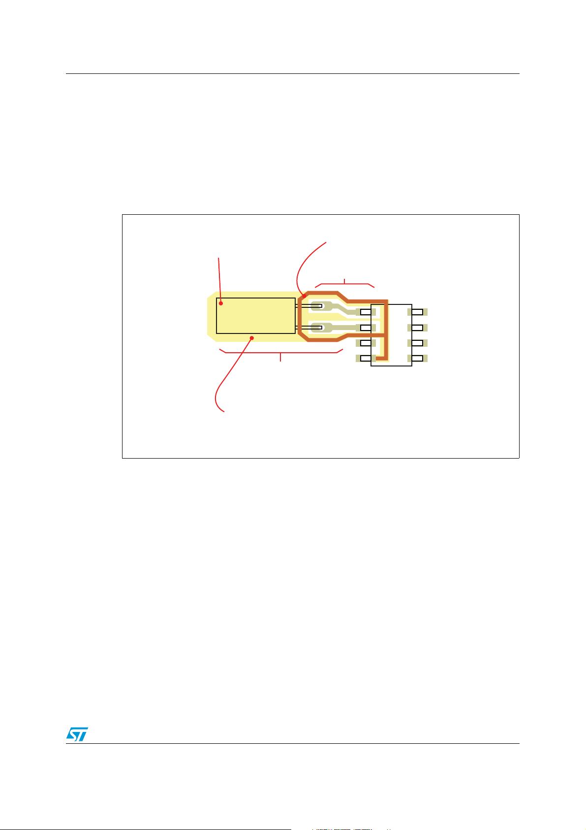
1 Layout considerations
1.1 What are some basic layout considerations for the RTC crystal?
Layout considerations are straightforward for the 32 KHz crystals used with ST's M41 series
real-time clocks.
Figure 1. Layout considerations
MOUNT CRYSTAL AS CLOSE
TO RTC AS POSSIBLE
CRYSTAL
NO OTHER COMPONENTS
REQUIRED IN OSCILLATOR
CIRCUIT
IF POSSIBLE, ADD LOCAL GROUND PLANE,
ON SEPARATE LAYER, ISOLATED FROM PCB
GROUND PLANE, AND CONNECTED TO
RTC GND PIN
ADD GUARD RING AROUND
CRYSTAL CONNECTIONS,
CONNECT TO GND PIN
KEEP TRACES SHORT
XI
RTC
XO
GND
AM04719v1
The primary consideration is lead length. The crystal should be mounted as near as
possible to the RTC to keep the traces short. A guard ring around these connections,
connected to ground, is very important to avoid picking up unwanted noise, which might
affect timekeeping.
Users should avoid running signals directly underneath this area unless a ground plane
resides between the signals and the crystal connections.
When possible, users can add an island ground plane under the area of the ring and crystal
body. This plane is on a separate layer from the ring, and isolated from the PCB ground
plane. It connects to ground at the GND pin of the RTC.
No other components are shown in the layout because the crystal is all that is required for
the RTC oscillator to work. No external load capacitors or bias resistors should be added.
Doc ID 16253 Rev 2 5/23
Page 6
Oscillator circuit AN3060
2 Oscillator circuit
2.1 Besides the crystal, what other components do I need to add to make my RTC oscillator work correctly?
None. Nothing else is required. ST's real-time clocks have built-in load capacitors.
External load capacitors are not needed, nor are external resistors. All that is needed is the
crystal. It must be a 32,768 Hz watch crystal and be rated for the load capacitance built into
the RTC.
Figure 2. Built-in load capacitors
EXTERNAL LOAD CAPACITORS
NOT NEEDED
EXTERNAL RESISTOR
NOT NEEDED
No other components are required to make the oscillator run. Adding any external
components will only serve to reduce the accuracy and reliability of the oscillator. Extra load
capacitors will tend to slow the clock. At low temperatures, such capacitance, or any
external resistance, may keep the oscillator from starting.
CRYSTAL
C
X1
R
X
XI XO
INTERNAL RTC
CIRCUITRY
C
L1
CHOOSE CRYSTAL TO MATCH RTC’S RATED
LOAD CAPACITANCE - eg, 6pF OR 12.5pF
C
L2
THEY ARE BUILT INTO RTC
C
X2
AM04720v1
Matching load capacitance
Each RTC comes with built-in load capacitors. These are usually specified as 12.5 pF, or in
the case of the M41T6x family, 6 pF. The crystal selected for use with the RTC should have
this same rating. Mismatched crystals will tend to run slightly off frequency. For example, a
crystal rated for 12.5 pF expects to see that load. If it is used with an RTC rated for 6 pF, the
crystal will only see 6 pF instead of the specified 12.5 pF and will thus run fast.
6/23 Doc ID 16253 Rev 2
Page 7

AN3060 Oscillator circuit
Effective load capacitance value versus internal capacitance value
Occasionally, the reader will see a reference to the individual load capacitors. There are two
used inside the RTC - one on each leg of the crystal. The actual value of each is twice the
rated or effective load value - that is, twice the load value specified in the data sheet. This is
because the internal load capacitors add in series. In Figure 2, the effective load
capacitance is:
CC
•
L
L
2
LL
1
CwithseriesinCC
1
==
L
2
CC
+
L
L
2
1
Thus, when C
the data sheet - is half of C
and CL2 are equal, the effective load capacitance, CL - the value listed in
L1
and CL2. An ST RTC rated for 12.5 pF will have two 25 pF
L1
capacitors built into its oscillator circuit. The reader is encouraged to be aware of this.
Furthermore, the reader should keep in mind that the crystal specifications should match
the rated value - in this case 12.5 pF - and not the individual values.
Doc ID 16253 Rev 2 7/23
Page 8

Undershoot AN3060
3 Undershoot
3.1 Can undershoot affect operation of my real-time clock? How? What can be done to guard against it?
Inherent in all field effect devices - all CMOS devices - are parasitic diodes resulting from the
intersection of P and N type regions in the device. Every PN junction forms a diode which
will conduct under any condition which biases the P region above the N region.
In Figure 3, if V
drawing current through the device. Significant undershoot on V
drops sufficiently below ground, the parasitic diode will be turned on thus
CC
can result in enough
CC
current flow to cause some disturbance in the real-time clock registers and hence can
adversely affect timekeeping. Therefore, undershoot should be avoided.
Figure 3. Typical parasitic diode
V
CC
D
N+
G
N
S
N+
Most ST real-time clocks specify a minimum V
undershoot to 0.3 V below ground.
Some supplies ramp very quickly when power cycling with the result that ringing can occur
which produces an undershoot condition that can cause problems for real-time clocks.
In the rare situations where this occurs, the best protection is a back biased Schottky diode
on the V
pin as shown in Figure 4. This addition has been shown to be a very reliable fix
CC
for undershoot problems.
P
of –0.3 V thereby limiting negative
CC
AM04721v1
Figure 4. Undershoot protection
V
CC
1N5817 (through hole)
BAT54J (surface mount)
8/23 Doc ID 16253 Rev 2
V
XI
XO
SDA
SCL
V
RTC
CC
SS
AM04722v1
Page 9

AN3060 Switchover voltage
4 Switchover voltage
4.1 Does the switchover voltage depend on the battery level? Or is it always a fixed value? What is the maximum battery voltage for an RTC?
Figure 5. Typical switchover circuits
V
CC
V
V
BAT
V
SO
With fixed reference
Power fail deselect voltage, V
CC-INT
PFD
V
When VCC falls to the power-fail deselect level, V
BAT
PFD
V
CC
V
CC-INT
V
SO
With battery reference
AM04723v1
, the part deselects thereby cutting off
communications to the host; it is write protected.
For ST's serial real-time clocks, V
voltage, V
Switchover voltage, V
. Thus, the deselect and switchover operations are tightly coupled.
SO
SO
is either equal to - or a function of - the switchover
PFD
Switchover connects the backup supply - usually a battery, but sometimes a capacitor or
super-cap - to the internal V
in the absence of system power. V
V
.
BAT
of the device thereby maintaining the timekeeping operation
CC
is the value of VCC at which the part switches over to
SO
Fixed reference
Most ST serial real-time clocks use a fixed, precision reference for the switchover threshold.
Regardless of the level of V
V
levels.
CC
the part will always deselect and switchover at the same
BAT,
Battery reference
Some older RTCs use the battery as a reference. One diode drop is applied, internal to the
RTC, to the battery pin, and that level determines the switchover threshold. Typically, the
diode drop is 0.5 V, but it can vary from 0.3 to 0.8 V. For brand new lithium coin cell
batteries, the voltage output may be as high as 3.5 V. (Once under load for a while, this will
drop to approximately 3.0 V and remain there for the useful life of the battery.) At low
temperatures, the diode drop will tend toward the minimum value, 0.3 V. This means that,
with new batteries and low temperatures, the switchover threshold may be as high as
3.5 - 0.3 = 3.2 V. The implication is that parts employing battery references may be
problematic in 3.3 V applications, and will be unsuitable for 3.0 V applications. In those
cases, users should choose parts with fixed references. For example, the M41T81S with
Doc ID 16253 Rev 2 9/23
Page 10

Switchover voltage AN3060
fixed reference is well-suited for 3.3 V and 3.0 V applications, and is a drop-in replacement
for the older M41T81 (non-S).
Table 1. Summary of deselect and switchover thresholds
Root part
number
M41T00 V
V
PFD
– 0.5 V
BAT
M41T00AUD 2.8
M41T00S 2.6 V
M41T11 V
– 0.5 V
BAT
M41T56 1.25 x V
M41T81 V
– 0.5 V
BAT
M41T81S 2.6 V
M41T82 V
M41T83 V
RST
RST
Switchover and deselect parameters
V
SO
– 0.5 V
BAT
(1)
(1)
BAT
2.0 < V
V
BACK
V
V
V
V
BACK
BAT
BAT
BAT
BAT
< V
PFD
> V
PFD
< V
PFD
> V
PFD
– 0.5 V
BAT
V
BAT
– 0.5 V
BAT
< V
PFD
> V
PFD
(1)
V
RST
(1)
V
RST
: V
: V
: V
: V
: V
: V
PFD
BAT
PFD
BAT
PFD
BACK
M41ST85W 2.6 V 2.5 V V
M41ST87W
M41T93 V
2.62 V, THS = 0
2.88 V, THS = 1
(1)
RST
2.5 V V
(1)
V
RST
M41T94 2.6 V 2.5 V V
1. The reset voltage, V
, can be specified as 2.32, 2.63 or 2.93 V.
RST
V
BAT-MAX
CC
V
CC
V
CC
CC
3.5 V
CC
V
CC
V
CC(max)
V
CC(max)
CC(max)
CC(max)
V
CC(max)
CC(max)
Complex switchover thresholds
Some devices employ more sophisticated switchover circuits which select the lesser of V
and V
as possible before switching over to the backup supply thus extending the backup life
slightly.
Figure 6. Switchover circuit
10/23 Doc ID 16253 Rev 2
as the switchover threshold. This ensures that the part remains on VCC for as long
BAT
V
BAT
PFD
V
CC
V
CC-INT
V
SO
AM04724v1
Page 11

AN3060 Switchover voltage
Maximum battery levels
The maximum value for V
varies within ST's family of serial RTCs. It is a function of the
BAT
process used to fabricate the silicon and considerations made during the design process.
For most parts, the maximum value is V
For parts with V
as the limit, if V
CC
exceeds VCC, parasitic diodes, inherent in CMOS
BAT
CC(max)
(usually 5.5 V).
technology, can be turned on thereby causing problems within the devices. Obviously, it is
okay for V
mode, V
To be clear, when V
and not V
regardless of the operating level of V
to be above VCC during backup (when VCC is 0). But when operated in active
BAT
should not exceed VCC for these parts.
BAT
CC-MAX
is the listed limit for V
CC
. Conversely, when the limit is V
.
CC
, the limit is the actual working level of VCC
BAT
CC(max)
, the V
limit is V
BAT
CC(max)
Doc ID 16253 Rev 2 11/23
Page 12

Oscillator fail detect AN3060
5 Oscillator fail detect
5.1 What is the OF bit? How does it work?
OF is the oscillator fail bit, and is set whenever the real-time clock detects approximately 4 to
6 consecutive missing pulses in the 4 KHz tap of the divider chain.
Figure 7. Oscillator fail detect circuit
CRYSTAL
OSCILLATOR FAIL DETECT CIRCUIT
V
CC
SET
Q
OF
AM04725v1
OSC TFF
(÷ 2)
TIME CONSTANT
SET TO 4-6 PULSES
TFF
(÷ 2)
TFF
(÷ 2)
4KHz
An RC circuit is used as an integrator. The 4 KHz pulses keep it discharged, and it slowly
charges between pulses. If sufficient pulses are missing, it charges high enough to trip the
comparator and set the OF bit. In the figure above, at low operating voltages, the time
constant will be shorter since the threshold voltage will be lower. Thus, fewer missing
pulses may be required to trigger the OF bit.
The basic mission of the OF function is to indicate when the oscillator has slowed or
stopped as might occur in capacitor backed applications or when the backup battery is
failing. When the backup voltage falls low enough, the part may stop keeping time, but the
registers will not necessarily become reset; the voltage may not drop low enough to
completely reset the part. Subsequently, after power-up, the oscillator will begin running
and, by merely reading the registers, it will not be clear that the timekeeping function had
become halted. The OF bit overcomes this. It provides a way for the system software to
monitor the timekeeping function and know when to advise the end user that the time may
need to be adjusted.
At first power-up, or anytime the oscillator has been turned off via the stop bit, the RC circuit
will be charged, and the OF bit will be set. The user should allow the oscillator to run for four
seconds prior to clearing the OF bit. This is done not only to discharge the RC circuit but to
ensure the oscillator has stabilized.
12/23 Doc ID 16253 Rev 2
Page 13

AN3060 Battery low detect
6 Battery low detect
6.1 How does the battery low bit work? Can it detect a missing battery?
Table 2. M41T81S register map
Addr
D7 D6 D5 D4 D3 D2 D1 D0
Function/range
BCD format
00h 0.1 seconds 0.01 seconds Seconds 00-99
01h ST 10 seconds Seconds Seconds 00-59
02h 0 10 minutes Minutes Minutes 00-59
03h CEB CB 10 Hours Hours (24-hour format) Century/hours 0-1/00-23
04h 0 0 0 0 0 Day of week Day 01-7
05h 0 0 10 date Date: day of month Date 01-31
06h 0 0 0 10M Month Month 01-12
07h 10 years Year Year 00-99
08h OUT FT S Calibration Calibration
09h OFIE BMB4 BMB3 BMB2 BMB1 BMB0 RB1 RB0 Watchdog
0Ah AFE SQWE ABE Al 10M Alarm month Al month 01-12
0Bh RPT4 RPT5 AI 10 date Alarm date Al date 01-31
0Ch RPT3 HT AI 10 hour Alarm hour Al hour 00-23
0Dh RPT2 Alarm 10 minutes Alarm minutes Al min 00-59
0Eh RPT1 Alarm 10 seconds Alarm seconds Al sec 00-59
0Fh WDF AF 0
BL 0 OF 0 0 Flags
10h 0 0 0 0 0 0 0 0 Reserved
11h 0 0 0 0 0 0 0 0 Reserved
12h 0 0 0 0 0 0 0 0 Reserved
13hRS3RS2RS1RS0 0 0 0 0 SQW
Many ST serial real-time clocks include a battery monitor function which sets the BL bit
when the battery is low. The basic functionality is to periodically compare the battery to the
internal 2.5 V reference and set the BL bit whenever the battery voltage is less than 2.5 V.
Figure 8. Battery monitor function
AT ROLLOVER &
AT POWER-UP
V
BAT
AT ROLLOVER
2.5V
AT ROLLOVER &
AT POWER-UP
Doc ID 16253 Rev 2 13/23
DBL
Q
AM04726v1
Page 14

Battery low detect AN3060
Periodic checking
The battery is checked every time the RTC powers up from backup mode, and every time
the clock rolls over at midnight (when not in backup mode). During the rollover check, the
battery is loaded to ensure a valid reading.
Power-up check
When an RTC has been in backup mode, its battery has already been loaded and thus a
load is not needed for the battery check. Batteries have a slow enough recovery time that
their outputs will not change quickly so it is not necessary to load them during the power-up
check. Nevertheless, a few devices - the M41T82, M41T83, M41ST87W and M41T93 include loading during the power-up check.
Detecting no battery - open circuit
Some applications call for being able to determine that no battery is installed. Ideally, a no
battery condition should read as low battery, but when the battery input, V
floated - the comparator output will be indeterminate. In order to reliably detect a no battery
condition, a load needs to be applied to the battery node prior to checking it. A resistor
applied across the battery terminals (or between B+ and ground in the case of devices with
no B– pin) is sufficient load for this purpose. This is impractical in the field, but can be useful
in the lab during development.
, is left open -
BAT
Using rollover to load the battery
Since the RTC applies a load to the battery during the midnight rollover check, it is possible
for applications to invoke the load by changing the time to near midnight, letting the clock
rollover, then setting the time back to its previous setting plus some delta to account for the
time spent waiting for rollover. This can be helpful during factory test to check that a battery
has been installed.
For example, if it's 17:53:27, the user would store that value, set the clock to 23:59:59, wait
two seconds, read the BL bit, then set the time back to 17:53:29 (17:53:27 + 2 seconds). In
this manner, the battery will be loaded during the check and thus a no battery condition will
be reliably read as battery low.
As stated above, some RTCs do load the clock during power-up, and thus a missing battery
can be detected by simply power-cycling the device.
14/23 Doc ID 16253 Rev 2
Page 15

AN3060 Halt (HT) bit
7 Halt (HT) bit
7.1 What does the halt bit (HT) do? How do I use it?
Table 3. M41ST85W register map
Address
00h 0.1 seconds 0.01 seconds Seconds 00-99
01h ST 10 seconds Seconds Seconds 00-59
02h 0 10 minutes Minutes Minutes 00-59
03h CEB CB 10 hours Hours (24 hour format) Century/hours 0-1/00-23
04h TR 0 0 0 0 Day of week Day 01-7
05h 0 0 10 date Date: day of month Date 01-31
06h 0 0 0 10M Month Month 01-12
07h 10 years Year Year 00-99
08h OUT FT S Calibration Control
09h WDS BMB4 BMB3 BMB2 BMB1 BMB0 RB1 RB0 Watchdog
0Ah AFE SQWE ABE Al 10M Alarm month Al month 01-12
0Bh RPT4 RPT5 AI 10 date Alarm date Al date 01-31
0Ch RPT3
0Dh RPT2 Alarm 10 minutes Alarm minutes Al min 00-59
0Eh RPT1 Alarm 10 seconds Alarm seconds Al sec 00-59
0Fh WDF AF 0 BL 0 0 0 0 Flags
10h00000000Reserved
11h00000000Reserved
12h00000000Reserved
13h RS3 RS2 RS1 RS0 0 0 0 0 SQW
D7 D6 D5 D4 D3 D2 D1 D0
HT AI 10 hour Alarm hour Al hour 00-23
Data
Function/range
BCD format
Many of ST's serial real-time clocks include a halt bit (HT) in the registers. This bit is used to
halt updates to the user clock registers. When HT is set, the internal counters continue
timekeeping, but the buffer/transfer registers accessed by the user are frozen.
Doc ID 16253 Rev 2 15/23
Page 16

Halt (HT) bit AN3060
Figure 9. Clock and non-clock registers
32KHz
OSC
DIVIDE BY
32768
1 Hz
SPI / I2C
SERIAL BUS
SERIAL
TRANSFER
REGISTER
READ / WRITE
BUFFER
TRANSFER
REGISTERS
SECONDS
MINUTES
HOURS
DAY-OF-WEEK
DATE
MONTHS
YEARS
CENTURIES
COUNTER
COUNTER
COUNTER
COUNTER
COUNTER
COUNTER
COUNTER
CLOCK COUNTERS
ARE BUFFERED VIA
BUFFER/TRANSFER
REGISTERS
NON-CLOCK REGISTERS
ARE DIRECTLY ACCESSED
Coherency
The clock counters are buffered to ensure coherency. At the start of a read of the clock
registers, the device will copy the counters to the buffer/transfer registers, then make no
further updates to these registers for the duration of the read cycle. (The HT bit is not set at
this time, but the updates are halted.) By copying all the counters simultaneously, the values
in the registers will all be from the same instant in time and thus will be coherent.
Example of incoherency
Without having the intervening buffer/transfer registers, if the user began directly reading the
counters at 23:59:59, a read of the seconds register would return 59 seconds. After the
address pointer incremented, the next read would return 59 minutes. The next read should
return 23 hours, but if the clock happened to increment between the reads, the user would
see 00 hours. When the time was re-assembled, it would appear as 00:59:59, and thus be
off by one hour. It would be incoherent.
WRITE FLAG
HALT BIT
NON-CLOCK
REGISTERS
SQUAREWAVE
CALIBRATION
WATCHDOG
COUNTER
WRITES TO ANY
CLOCK REGISTER CAUSE
WRITE FLAG TO BE SET.
AT END OF WRITE CYCLE,
IF WRITE FLAG IS SET,
BUFFER/TRANSFER
REGISTERS COPIED TO
COUNTERS
AM04727v1
By using the buffer/transfer registers to hold a copy of the time, the user is able to read the
entire set of registers without any values changing during the read.
Similarly, when the application needs to change the time in the counters, it is necessary that
all the counters be loaded simultaneously. Thus, the user writes sequentially to the various
buffer/transfer registers, then they are copied to the counters in a single transfer thereby
coherently loading the counters.
16/23 Doc ID 16253 Rev 2
Page 17

AN3060 Halt (HT) bit
Write flag
The copying to the counters is caused by an internal write flag which gets set anytime a
write occurs in one of the buffer transfer registers, but not to any of the other (non-clock)
registers. For example, writing the watchdog or calibration register will not set the write flag,
but writing the seconds or day-of-week will set the flag.
At the end of the write cycle, when a STOP condition occurs on the I
sees the write flag set, it copies all the buffer transfer registers to the clock counters. Even if
only one or two of the buffer/transfer registers is over-written by the application, all the
registers will be copied to the counters.
2
C bus, if the device
Auto-setting of the HT bit
Whenever the device is powered down, the time and date are copied to the buffer/transfer
registers and the HT bit is set automatically. At power-up, the user can read the device (with
the HT bit still set) and retrieve the time of power-down from the registers. This allows the
application to determine how long the power outage lasted which is needed in some
situations. As long as the HT bit remains set, reads will return the time of power-down
(assuming no writes have occurred to alter the contents of the buffer/transfer registers).
In order to read the present time, the user must first clear (write a 0 to) the HT bit.
Subsequent reads will return the current time. Subtracting the time of power-down from the
present time establishes the length of the power outage.
Writing with the HT bit set
Following a power failure, the buffer/transfer registers contain the time of power-down.
Should the user write to any of the clock registers (addresses 0x00 to 0x07 in the table
above), the write flag will be set. Thus, at the end of the write cycle, the counters will be
updated from the registers.
If the HT bit is still set, the buffer/transfer registers contain the time of power-down modified
by the written value. Thus, at the end of the write sequence, the modified time of powerdown will be written back into the counters thus causing an apparent loss of time.
Example: Let the time/date of power down be, Mon, 9-Mar-08, 7:23:44pm. At power-up,
prior to clearing the HT bit, the user writes the ST bit in the seconds register thus setting the
write flag, but writes no other bits. At the end of the write cycle, the present time will revert
to the time of power-down thus resulting in an apparent loss of time.
Conversely, if the HT bit had been cleared prior to the write, the buffer/transfer registers
would have been updated to the present time. As before, a write of the ST bit would have
set the write flag, but the resultant update of the counters would have placed the current
time back in them. They would have been written over with the same values already present
in the counters. No loss of time would occur.
For more information, refer to application note AN1572.
Doc ID 16253 Rev 2 17/23
Page 18

RTC initialization AN3060
8 RTC initialization
8.1 What is the best sequence for accessing the RTC at first power-up? On subsequent power-ups?
This will vary from device to device, and hence a comprehensive answer is beyond the
scope of this document. Instead, we offer an example for the M41T83/M41T82.
Initializing and accessing the M41T83/M41T82
At first power-up, the part is in a benign state - the alarms and interrupts are disabled as are
the watchdog and timer. The OUT bit is high, and the frequency test bit, FT, is disabled.
Both the digital and analog calibration functions are set to the neutral points and the OTP bit
is set to 0 thus selecting the user analog calibration register over the factory value. (OTP
applies only to the M41T83 in the embedded crystal [MY] package.)
The squarewave output is enabled and 32.768 kHz is selected. (This allows devices using
this as a reference to have it at first power-up without need of user intervention.)
Figure 10. M41T83/M41T82 power-up defaults
ST HT CB1:CB0 OUT FT
1st power-up 0 1 00 1 0 0000000 0 1 0 0 00000 0 0 0 11
Power-up from
backup
1st power-up
Power-up from
backup
UC 1 UC UC 0 0000000 UC UC UC UC UC 0 UC UC UC
Digital Cal
DCS, DC4:DC0
000000 00000000
UC UC
Analog Cal
ACS, AC5:AC0
Watchdog
BM4:BM0,
RB1:RB0
OSC Fail Alarm 1 Timer
OFIE OF
Squarewave output Alarm 2
SQWE RS3:RS0 OTP AL2E
1 1000 0 0 0 00000
UC UC UC UC UC UC
IRQ1/FT/OUT pin
A1IE
ABE RPT15:11 TE
A2IE
RPT25:21
TI/TP
TIE
TD1:TD0
The clock registers - hours, minutes, seconds, year, month, date - are unknown. Only the
century bits, CB1:CB0, are defined (00).
The stop bit, ST, powers up cleared thus enabling the 32 KHz oscillator. But, since the
oscillator has not been running (prior to this first power-up) the oscillator fail detect bit, OF,
will be set.
Lastly, as is the case at all power-ups, the HT bit is set.
AM04728v1
18/23 Doc ID 16253 Rev 2
Page 19

AN3060 RTC initialization
First power-up
Since most of the peripheral and alarm functions are not enabled at power-up, there is little
urgency to initialize the part. The only item which might require immediate attention is the
squarewave function which powers-up running. Some applications may prefer to disable
this, or change its frequency.
The next thing the user should do is to write the HT bit to 0, then set the time and date. (For
other RTCs, at this point in the flow, if the ST bit is 1, it should be cleared to 0.)
If the application will be calibrated, this should be the next step.
Then the OF bit should be cleared (written to 0). Since power-up - since oscillator startup four seconds must have elapsed before this step is done. If calibration was performed, then
the time required to do that can be subtracted from the four seconds, and if calibration took
longer than that, then no additional waiting is required. The software should verify that the
OF bit remained cleared before progressing to the next step.
The next few items are optional. If the watchdog will be used, it can be started now,
assuming the software will soon get to the operational code which updates the watchdog.
Otherwise, the software should wait until the top of its main routine to start the watchdog.
If the timer or alarms will be used, the user might set them here, or again wait until the top of
the main routine. That will prevent any of these functions from timing out (interrupting) while
the processor is still running its initialization routine.
Doc ID 16253 Rev 2 19/23
Page 20

RTC initialization AN3060
Figure 11. First power-up
st
1
power-up
Optional: Change Squarewave
frequency or disable it.
Clear HT bit
Write hours, minutes, seconds,
day-of-week, date, month, year
and century bits.
Optional: Set OTP to 1 to select
factory analog calibration
(M41T83-MY only).
Optional: Initialize analog or
digital calibration.
Wait 4 seconds, then clear OF bit.
Verify OF bit is clear.
Optional: Initialize watchdog.
Optional: Initialize timer.
Optional: Initialize alarm 1.
Optional: Initialize alarm 2.
END
AM04729v1
20/23 Doc ID 16253 Rev 2
Page 21

AN3060 RTC initialization
Power-up from backup
Coming out of backup, the first thing to do is read the time. Prior to clearing the HT bit, the
RTC's buffer/transfer registers will contain the time of power down. If the duration of power
outage is needed by the application, the time of power down will be required. Otherwise,
this step can be skipped.
The next step is to clear the HT bit by writing it to 0. It is very important that the HT bit be
cleared prior to writing any of the timekeeping registers (addresses 0x00 to 0x07). Failure to
do so can resulting in corrupting the RTC counters.
If, at this point in the application flow, the present time is required, the time would be read.
With the HT bit clear, the present time will be returned by a read.
Upon servicing any interrupts from the RTC - e.g., alarm or OF - the flags register must be
cleared. Most of the flag bits clear upon reading, but the OF bit must be written to 0. Also,
the user should bear in mind that clearing the alarm flags (AF1, AF2) and oscillator fail flag
(OF) will clear the associated interrupt.
Figure 12. Power-up from backup
Power-up from backup
Optional: Read time/date
(time of power-down).
Clear HT bit
Optional: Read time/date
(present time).
off_duration = present_time –
time_of-power-down
Clear any flags (read flags register)
Optional: Re-initialize watchdog.
Optional: Re-enable / Re-initialize
timer.
END
AM04730v1
Watchdog and timer
Lastly, power cycling always leaves the watchdog and timer disabled. If either is being used
by the application, they will need to be re-initialized.
Doc ID 16253 Rev 2 21/23
Page 22

Revision history AN3060
9 Revision history
Table 4. Document revision history
Date Revision Changes
04-Nov-2009 1 Initial release.
17-Jul-2012 2 Textual updates concerning device availability.
22/23 Doc ID 16253 Rev 2
Page 23

AN3060
Please Read Carefully:
Information in this document is provided solely in connection with ST products. STMicroelectronics NV and its subsidiaries (“ST”) reserve the
right to make changes, corrections, modifications or improvements, to this document, and the products and services described herein at any
time, without notice.
All ST products are sold pursuant to ST’s terms and conditions of sale.
Purchasers are solely responsible for the choice, selection and use of the ST products and services described herein, and ST assumes no
liability whatsoever relating to the choice, selection or use of the ST products and services described herein.
No license, express or implied, by estoppel or otherwise, to any intellectual property rights is granted under this document. If any part of this
document refers to any third party products or services it shall not be deemed a license grant by ST for the use of such third party products
or services, or any intellectual property contained therein or considered as a warranty covering the use in any manner whatsoever of such
third party products or services or any intellectual property contained therein.
UNLESS OTHERWISE SET FORTH IN ST’S TERMS AND CONDITIONS OF SALE ST DISCLAIMS ANY EXPRESS OR IMPLIED
WARRANTY WITH RESPECT TO THE USE AND/OR SALE OF ST PRODUCTS INCLUDING WITHOUT LIMITATION IMPLIED
WARRANTIES OF MERCHANTABILITY, FITNESS FOR A PARTICULAR PURPOSE (AND THEIR EQUIVALENTS UNDER THE LAWS
OF ANY JURISDICTION), OR INFRINGEMENT OF ANY PATENT, COPYRIGHT OR OTHER INTELLECTUAL PROPERTY RIGHT.
UNLESS EXPRESSLY APPROVED IN WRITING BY TWO AUTHORIZED ST REPRESENTATIVES, ST PRODUCTS ARE NOT
RECOMMENDED, AUTHORIZED OR WARRANTED FOR USE IN MILITARY, AIR CRAFT, SPACE, LIFE SAVING, OR LIFE SUSTAINING
APPLICATIONS, NOR IN PRODUCTS OR SYSTEMS WHERE FAILURE OR MALFUNCTION MAY RESULT IN PERSONAL INJURY,
DEATH, OR SEVERE PROPERTY OR ENVIRONMENTAL DAMAGE. ST PRODUCTS WHICH ARE NOT SPECIFIED AS "AUTOMOTIVE
GRADE" MAY ONLY BE USED IN AUTOMOTIVE APPLICATIONS AT USER’S OWN RISK.
Resale of ST products with provisions different from the statements and/or technical features set forth in this document shall immediately void
any warranty granted by ST for the ST product or service described herein and shall not create or extend in any manner whatsoever, any
liability of ST.
ST and the ST logo are trademarks or registered trademarks of ST in various countries.
Information in this document supersedes and replaces all information previously supplied.
The ST logo is a registered trademark of STMicroelectronics. All other names are the property of their respective owners.
© 2012 STMicroelectronics - All rights reserved
STMicroelectronics group of companies
Australia - Belgium - Brazil - Canada - China - Czech Republic - Finland - France - Germany - Hong Kong - India - Israel - Italy - Japan -
Malaysia - Malta - Morocco - Philippines - Singapore - Spain - Sweden - Switzerland - United Kingdom - United States of America
www.st.com
Doc ID 16253 Rev 2 23/23
 Loading...